Manh Cuong Tran1, Tuan Hung Ho1, Thuy Thi Nguyen1, Tran Minh Duc2
1Faculty of Physics, Hanoi National University of Education, Ha Noi, Viet Nam
2Faculty of Chemistry, Hanoi National University of Education, Ha Noi, Viet Nam
Correspondence to: Manh Cuong Tran, Faculty of Physics, Hanoi National University of Education, Ha Noi, Viet Nam.
| Email: |  |
Copyright © 2016 Scientific & Academic Publishing. All Rights Reserved.
This work is licensed under the Creative Commons Attribution International License (CC BY).
http://creativecommons.org/licenses/by/4.0/

Abstract
This paper presents first a simulation method to evaluate the electric field on the surface of a High Impedance Surface (HIS) structure using a monopole antenna working at Q band. The simulation bases on FDTD (Finite Difference Time Domain) code. Operating frequency of monopole antenna lies within the forbidden bandgap of HIS structure. The electric field on the surface of the structure within and outside the bandgap is observed and studied. These HIS structures then are applied to improve the performances of patch antenna which works in the same frequency band. The method can be used to evaluate the performance of HIS structure on antenna system.
Keywords:
Metamaterials (MTM), HIS, Monopole antenna, Electromagnetic bandgap, Reflection coefficient
Cite this paper: Manh Cuong Tran, Tuan Hung Ho, Thuy Thi Nguyen, Tran Minh Duc, Evaluating the Electromagnetic Surface Wave of High Impedance Structures by Monopole Antenna and Application for Patch Antennas at Q Band, International Journal of Electromagnetics and Applications, Vol. 6 No. 1, 2016, pp. 1-6. doi: 10.5923/j.ijea.20160601.01.
1. Introduction
High Impedance Surface or HIS is a metamaterial structure [1-4] formed by periodic metallic unit cells on a dielectric substrate. HIS possesses a forbidden electromagnetic frequency bandgap, in which the effective surface impedance of HIS is very high, therefore, the surface does not support surface wave [5-7]. One can take advantage of this interesting characteristic to improve the performances of electromagnetic structure designs by integrating them into the systems [5-9]. One can also apply metamaterial absorber in a similar concept to enhance the performance of antenna structure [10, 11]. Techniques to determine the electromagnetic bandgap of HIS structure is realized by simulation. In this study, we use the CST Microwave Studio (CST MWS) simulator, based on FDTD (Finite Difference Time Domain) code to observe graphically electromagnetic field on the surface of studied structure within and outside the bandgap of HIS.Q frequency band which ranges from 30-50 GHz is commonly used to serve multi-purposes in military and civilian lives like satellite communications, terrestrial microwave communications, radar, radio astronomy and mobile millimeter-wave radar research military radar targeting. Studying new electromagnetic materials in this band plays a vital role in modern electrical engineering. In this paper we first investigate the effect of HIS structure on the surface wave on the ground plane of Q-band monopole antenna. The HIS is used to isolate surface wave propagation from edges of the antenna substrate.HIS structure then is integrated into microstrip patch antenna designs. The microstrip antenna will be surrounded by a limited rows number of HIS unit cells. The HIS structure shows that it can be used to improve the performances of antenna. The HIS based antenna operates at Q frequency band and can be used for high data rate communication purpose. HIS based antenna prototypes have been fabricated and characterized to study the effects of the HIS structure on the performances of antennas. The return loss and radiation patterns of the HIS patch antenna prototypes are compared to the conventional design in order to bring out the role of HIS.
2. HIS with Monopole Antenna
In this paper, electric field on the surface of HIS structure within and outside the forbidden bandgap is observed. From the simulation, one can see HIS can help to eliminate the surface waves of antenna, which improves the performances of antenna. A monopole antenna working at 39.5 GHz is used in the study. This kind of antenna is one of the simplest antennas, as shown in Figure 1. Monopole antenna can be created easily by extending the center core of the coaxial cable. The metallic shield of the cable is connected with ground plane. 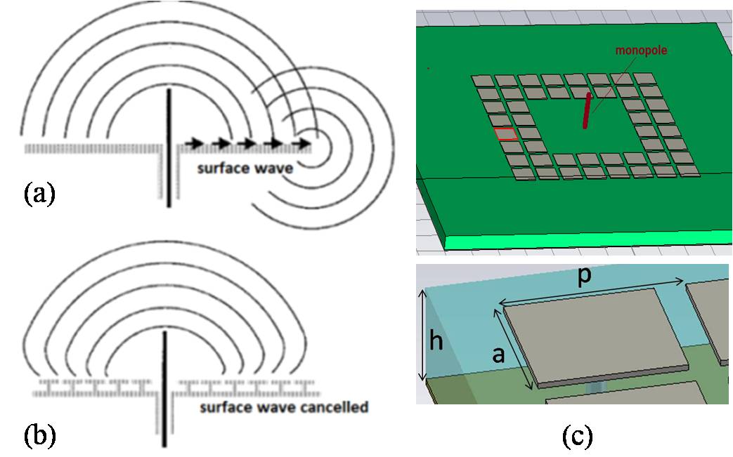 | Figure 1. (a) Conventional monopole antenna, (b) Surface waves are cancelled with the HIS structure, (c) Perspective view of monopole MTM antenna and dimension of HIS unit cell in the simulation |
On an infinitely large ground plane, such monopole antenna has a radiation pattern with a zero on the axis of the antenna and no backward-waves. In fact, the ground plane is limited, and the edges of the plane contribute to radiation pattern (fringing-field). With the space waves, the antenna also generates surface waves on the ground plane, which then participate to the radiation from the edge and corners. The combination of the radiation of the antenna and the edge waves can form a series of side lobes, causing a significant loss of the radiation power.If the ground plane is replaced by a high-impedance surface (Figure 1b), the surface waves are suppressed [5, 7]. The induced surface currents are limited to a local region around the monopole antenna, and cannot reach the edge of the ground plane. This leads to less ripple radiation and less loss of backward wave power of antenna. In principle, the more elements of HIS are used, the lower level of surface waves is obtained [3, 7]. To study this characteristic, we consider three cases of monopole antenna with and without the integration of HIS structure to the ground plane. Three cases are simulated: (a) Only monopole (no HIS structure), (b) the monopole surrounded by 2×2 rows of HIS square cells and (c) the monopole surrounded by 5×5 rows of HIS square cells. We chose these cases in order to compare the behavior of the HIS based on numbers of elements used.The size of each square cell of HIS is a×a = 0.8mm×0.8mm and the period is p = 1mm as shown in Figure 1c. The substrate is Ro4450, with h = 0.51mm, permittivity εr = 3.58, loss tangent is 0,0016. With these parameters, the forbidden bandgap of HIS structure is calculated by CST MWS simulation and it is in the range of 34-41.5 GHz (Figure 2); we note that the resonant frequency of monopole is within the forbidden bandgap of HIS. 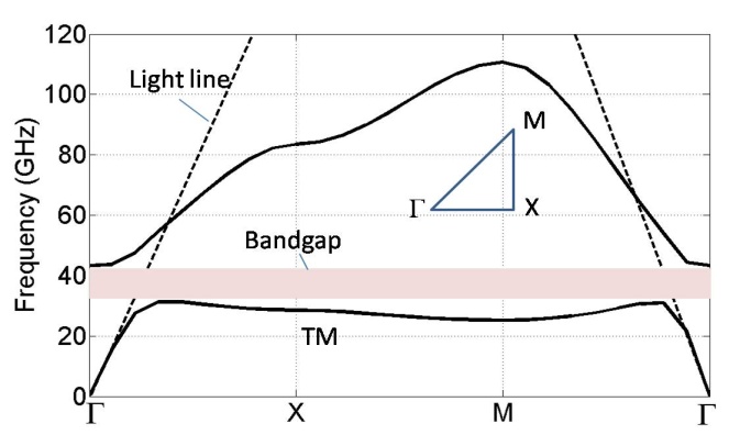 | Figure 2. Dispersion diagram of HIS structure |
Figure 3 indicates the reflection coefficient of monopole antenna used in this study, the resonant frequency is 39.5 GHz.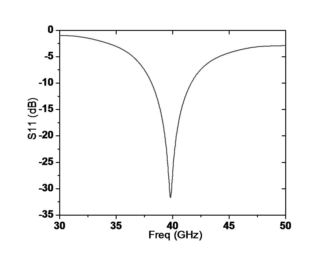 | Figure 3. Reflection coefficient of monopole antenna |
Figure 4 and Figure 5 presents the simulation results realized by CST Microwave studio package. Electric fields on the surface of HIS are observed graphically at different frequencies within and outside the resonance (corresponding to 39.5 GHz and 30 GHz). Figure 4 shows the observation side-view and top-view of the electric field of antenna for three cases: only monopole, the monopole surrounding by 2×2 HIS rows and the monopole surrounding by 5×5 HIS rows, the electric field is observed at the resonant frequency of monopole (39.5 GHz). The electric scale of the simulation is normalized to 10kV/ m. We see in Figure 4 that for the case in which monopole antenna surrounded by 5 rows of HIS on each side, the electric field in the edge and corner of ground plane is very weak compared to the case without HIS, especially in the case with 5 rows of HIS. This difference can be explained by the presence of the high impedance surface structure. These HIS structures suppress the propagation of surface waves. We observe the same results with the monopole antenna case surrounded by 2 rows each side but the level of wave suppression is lower. This confirms that the more HIS structures are used, the stronger level of surface wave suppression is obtained at the resonant frequency of antenna. 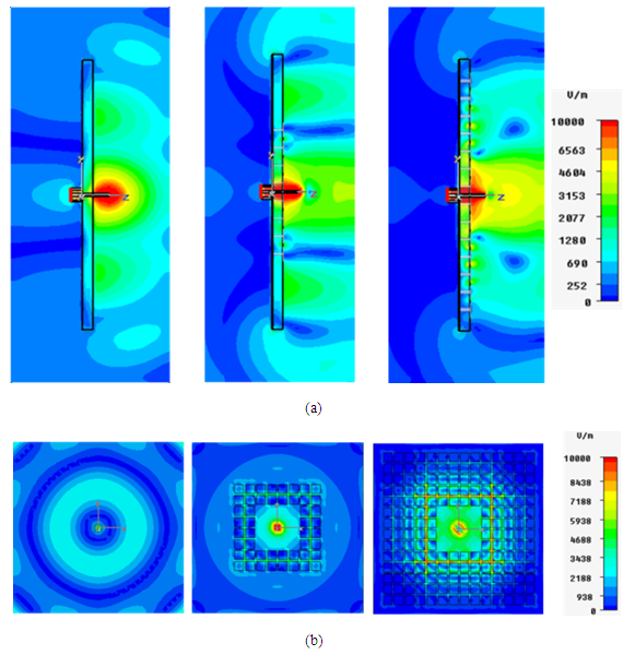 | Figure 4. (a) Electric field at the edges of antenna structures (side-view) and (b) near electric field on the antenna surface of 3 antennas (top-view), observed at resonant frequency (within the bandgap of HIS) |
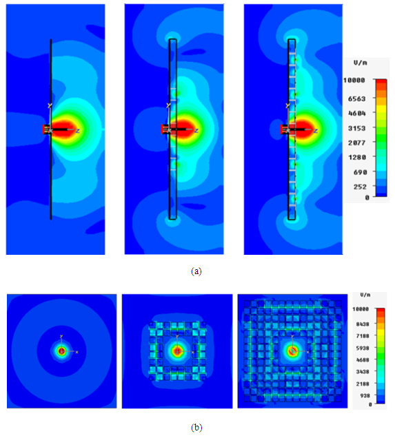 | Figure 5. (a) Electric field at the edge of antenna structures (side-view) and (b) near electric field on the antenna surface for 3 antennas (top-view), observed at 30 GHz (outside the bandgap of HIS) |
Figure 5 shows the side-view and top-view of surface waves observed at the frequency outside the electromagnetic bandgap of HIS (30 GHz). We see that in the case with 5 rows of HIS each side and the case with 2 rows each side, the electric fields at the edges of ground plane are about the same level with the case without HIS. This shows that if the working frequency is outside the bandgap, the surface waves can propagate freely on the surface of HIS structure and affect the radiation of antenna. From these comparisons, we can conclude that the surface wave suppression property can only appear inside the forbidden bandgap of HIS structure. By using this property, the integration of HIS on the ground plane of the monopole antenna or patch antenna can help to remove the surface waves, therefore, improves the performances of antenna.
3. Application for Patch Antenna
Patch antennas or microstrip antennas nowadays are becoming increasingly useful in the telecommunication market. These kinds of antennas are low cost, have a low profile and are easily fabricated. In this section, HIS structure is integrated to the ground plane of patch antenna and the performances of patch antenna are investigated.A conventional patch antenna which works at Q band frequency (39.5GHz) is used for the investigation. The size of antenna is 1,60 mm× 1,70 mm and the antenna is fed by a 50 Ω coaxial cable and a SMA connector. The same substrate of the HIS structure from the session above is used for patch antenna configuration. HIS structure is integrated to patch antenna to improve its performances. Two cases of metamaterial antennas are studied. HIS structure contains maximum of 13×13 unit cells. The patch antenna element remains located in the central position of the HIS region. The space between each side of the antenna with the HIS is created by removing 5 (antenna 1) and 6 (antenna 2) rows of HIS respectively from the center of the HIS structures (Figure 6). 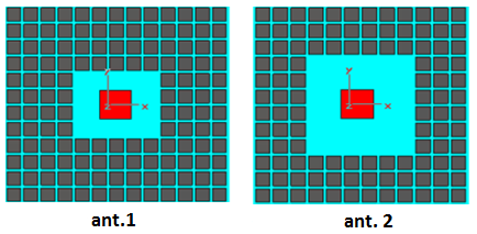 | Figure 6. Two metamaterial antennas (MTM antenna) in the simulation |
The simulation results of reflection coefficients S11 for conventional antenna, metamaterial antenna 1 and metamaterial antenna 2 are shown in Figure 7 respectively. Center resonant frequency is proximity 39,5 GHz. A shift of resonant frequency, which comes from the electromagnetic coupling of HIS elements with the radiation patch, is observed. If the distance between the HIS and the patch antenna is small (case 1), a strong coupling is obtained and the resonant frequency is shifted towards higher frequencies. A change in the dimension of the antenna can help to compensate the change of the resonant frequency, with a reminder that in this research, the size of the antenna is kept constant in all cases. We see that the bandwidth of MTM antenna is better (≈15%). In these configurations, the beginning radiation of the elements of HIS is caused by the strong electromagnetic coupling with the antenna radiations. The resonance modes of each cell of the HIS metal element are different from those of the main radiating element (patch antenna), the level of the resonance of the antenna falls and therefore, the bandwidth becomes broader. This principle can be used to increase the bandwidth of patch antenna in telecommunication applications.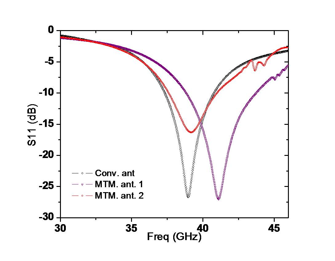 | Figure 7. Simulation results of reflection coefficient of three antennas |
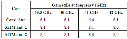
In Figure 8, the simulated radiation patterns of antenna are observed in the H-plane and E-plane in the frequency range of 39 - 42 GHz. Both the principle polarization (co-pol) and cross- polar (cr-pol) are plotted. When the distance between HIS and the radiating patch rises (case MTM ant.2), the antenna finds its initial adaptation and a better radiation pattern is observed. Also, the case of MTM antenna 2 (Figure 6) seems to be the best suited for our application because it supports the zero degree reflection phase on the largest surface area. The gain of the antenna at the resonance is optimized in this case (8.2 dB co-pol compared to 6.1 dB for the conventional case).The cross-polarization level on the radiation pattern of the HIS based antennas is lower than in the conventional case. The results from Figure 8 show that near the resonant frequency (at 39 GHz - the red curves), the cross-polarized radiation is decreased by using the HIS. In particular, the cross-polarization levels of MTM antennas at the direction of ±90 degrees are ordinary ≈8-10 dB lower than in the conventional case. A summary of antenna gain is given in Table 1. This shows that the performances of metamaterial antennas are improved, the gains of the MTM antenna are 2 dB higher than in the conventional case.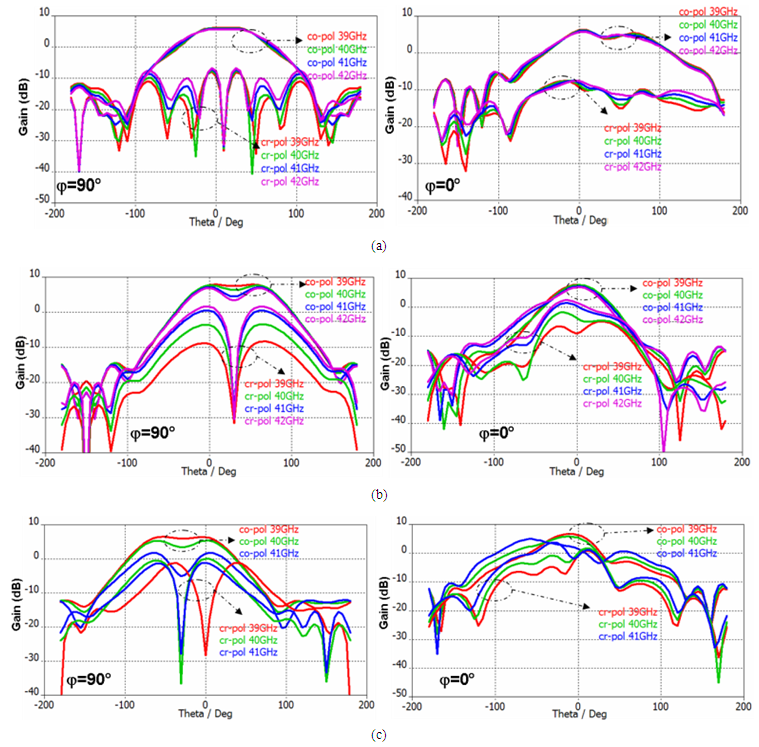 | Figure 8. Simulation radiation patterns of 3 antennas: (a) Conv. Antenna; (b) MTM antenna 1 and (c) MTM antenna 2 |
Table 1. Gains of antennas (for E plane)
 |
| |
|
As mentioned above, the designed of MTM antennas has been realized (Figure 9) for the verification. The HIS structure and microstrip antenna in the experiment is fabricated by photolithography technology. In this method light (ultraviolet) is used to etch the substrate behind a photo mask to make desired geometric pattern. This method produces highly accurate etched pattern of the substrate. The SMA connector is used to feed the patch antenna.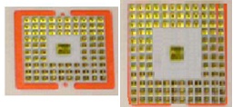 | Figure 9. The fabricated metamaterial antennas |
The measurement results of radiation pattern in the E plan for the principle polarization and reflection coefficient of three antennas are presented in Figure 10 and Figure 11 respectively. The measured resonant frequency of all antennas is around 39,5 GHz. In the experiment, the scan angle ranges from -90 to 90 degrees due to the limitation of device in our experiment. We see that the gain of MTM antenna cases is 2 dB higher compared to the conventional case, which shows a good agreement with the simulation results. 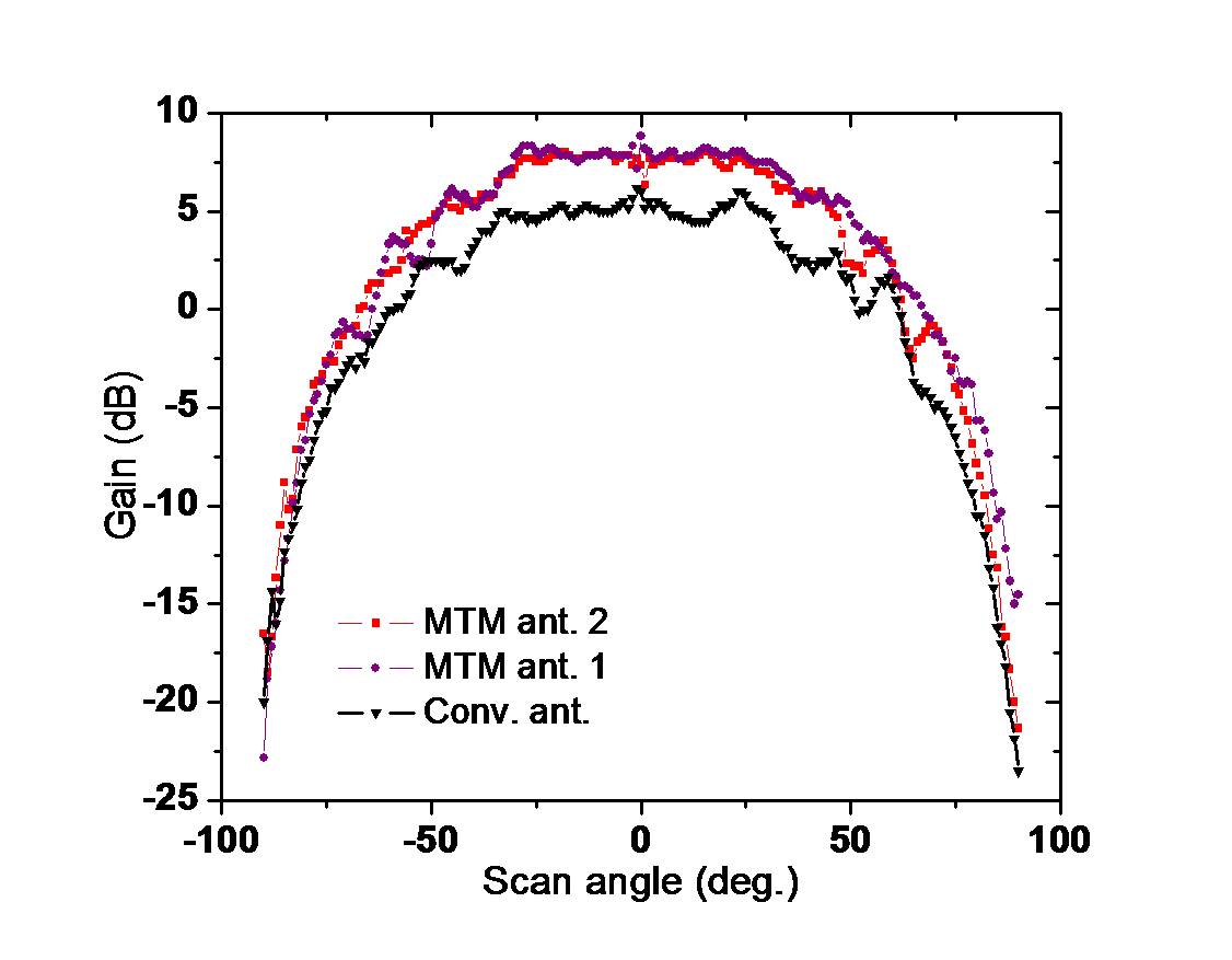 | Figure 10. Measurement results of gain of three antenna cases |
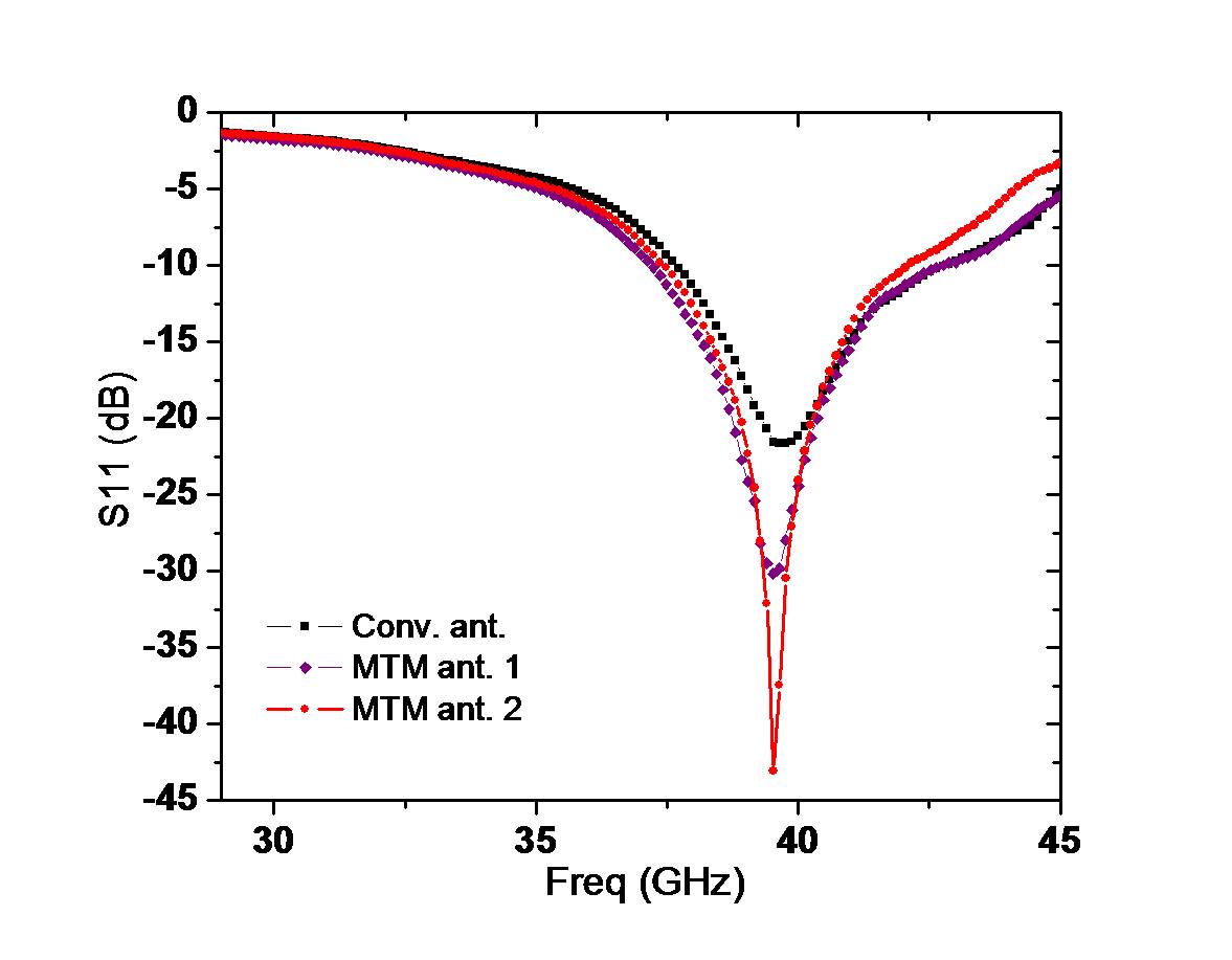 | Figure 11. Measurement results of reflection coefficient of three antennas |
4. Conclusions
A validation and application of HIS structure is performed using millimeter monopole antenna in this paper. By observing electromagnetic wave propagation on the ground plane surface of antenna structure, we see clearly the advantage of HIS for removing electromagnetic surface waves, which also helps to determine the electromagnetic bandgap of HIS structure. The optimized HIS structure is then applied to improve the performances of millimeter microstrip patch antenna. The simulation and experimental results show an attractive remark on gain and bandwidth of patch antenna: a high gain of 8,2 dB is obtained with a broadband frequency of 15%. A reduction of cross-polarized radiation at resonance is also obtained in simulation for MTM antennas. This application technique of High impedance surfaces can be used to improve the performances of antenna systems or further analyze the electromagnetic characteristics of microstrip antenna systems.
ACKNOWLEDGEMENTS
This research is funded by Vietnam National Foundation for Science and Technology Development (NAFOSTED Grant no.103.99-2011.02).
References
| [1] | V. G. Veselago, The electrodynamics of substances with simutaneously negative values of ε and µ. Soviet physics, Vol 10, 1968. |
| [2] | A. Alu and N. Engheta, Radiation from a Traveling-Wave Current Sheet at the Interface between a Conventional Material and a Material with Negative Permittivity and Permeability, Microwave and Optical Technology Letters, Volume 35, Issue 6, December 20, 2002. |
| [3] | D. Sievenpiper, L. Zhang, R. F. J. Broas, N. G. Alexopoulos, and E. Yablonovitch, High Impedance electromagnetic surfaces with a forbidden frequency band, IEEE Trans, Micro, Theory & Tech, vol. 47, 1999. |
| [4] | N. Engheta, An Idea for Thin, Subwavelength Cavity Resonators Using Metamaterials with Negative Permittivity and Permeability, IEEE Antennas and Wireless Propagation Letters, Volume 1, Issue 1, January, 2002. |
| [5] | F. Yang, Y. Rahmat Samii, Microstrip antennas intergrated with electromagnetic bandgap structure: A low mutual coupling design for array applications. IEEE Trans. ant. appl, vol. 51, no. 10, 2003. |
| [6] | H. Xin, K. Matsugatani, M. Kim, J. Hacker, J. A. Higgins, M. Rosker and M. Tanaka, Mutual coupling reduction of low-profile monopole antennas on high-impedance ground plane. Electronics letters, 1st August, Vol 38, No 16, 2002. |
| [7] | Sievenpiper, D, High impedance electromagnetic surfaces. PhD Dissertation, Electrical Engineering Departement. University of California at Los Angeles, Los Angeles, CA, 1999. |
| [8] | A. Ourir, Applications de Matériaux à Bandes Interdites Photoniques et de métamatériaux en Télécommunications. PhD Dissertation, Université de Paris XI d’Orsay, 2008. |
| [9] | P. Kovács, J. Puskely, Stacked High-Impedance Surface (HIS) for 5 GHz WLAN Applications. Radioengineering, Vol. 22, No. 1, April, 2013. |
| [10] | Sijia LI, Xiangyu Cao, Tao Liu, Huanhuan Yang, Double-layer Perfect Metamaterial Absorber and Its Application for RCS Reduction of Antenna, Radioengineering, Vol. 23, No. 1, 2014. |
| [11] | Hao Zhang, Xiang-Yu Cao, Jun Gao, Huan-Huan Yang, and Qun Yang, A Novel Dual-Band Metamaterial Absorber and Its Application for Microstrip Antenna, Progress In Electromagnetics Research Letters, vol. 44, 35- 41, 2014. |

 Abstract
 Reference
 Full-Text PDF
 Full-text HTML