International Journal of Electromagnetics and Applications

p-ISSN: 2168-5037    e-ISSN: 2168-5045

2014;  4(3): 57-60

doi:10.5923/j.ijea.20140403.01

Tunable Terahertz Metamaterial Absorbers Using Active Diodes

Limei Qi, Chao Li, Guangyou Fang

Key Laboratory of Electromagnetic Radiation and Detection Technology, Chinese Academy of Sciences, Beijing, China

Correspondence to: Limei Qi, Key Laboratory of Electromagnetic Radiation and Detection Technology, Chinese Academy of Sciences, Beijing, China.

Email:

Copyright © 2014 Scientific & Academic Publishing. All Rights Reserved.

Abstract

A tunable terahertz absorber based on voltage-controlled diodes has been designed. For each unit cell of the absorber, a terahertz active diode is used to connect two identical opposite meander-lines. Then, voltage can be applied to the diodes without incorporating an extra bias line to each unit, which greatly reduces the machining difficulty in the terahertz region. To give a physical insight into the tunable absorber, a transmission-line equivalent circuit is given and described. Through retrieving the real part and the imagery part of the relative impedance of the absorbers, we found that the absorption is dependent on the relative impedance, and the near-unity absorbance can be achieved when the impedance is more close to that of the free space.

Keywords: Terahertz, Metamaterial absorber, Active diode, Tunable

Cite this paper: Limei Qi, Chao Li, Guangyou Fang, Tunable Terahertz Metamaterial Absorbers Using Active Diodes, International Journal of Electromagnetics and Applications, Vol. 4 No. 3, 2014, pp. 57-60. doi: 10.5923/j.ijea.20140403.01.

1. Introduction

Terahertz (THz) radiation provides many useful applications for spectroscopy, biomedical imaging, security, food quality control and communication [1–2]. Since the very field of the THz science and technology is relatively young, new devices and materials are on demand. Metamaterials with peculiar electromagnetic properties have attracted considerable interest to terahertz devices in the last decade [3]. Recently, the Metamaterial absorber is an important application to metamaterials in microwave and terahertz [4], which typically consists of two metallic layers spaced apart by virtue of a dielectric spacer. The top metal layer is geometrically patterned in order to strongly couple to the incidence electric field. By pairing the top layer with a metal ground plane, a mechanism with impedance-match to that of free space may be created. Landy et al [5] firstly reported the concept of the perfect metamaterial absorbers and demonstrated the absorption of 88% in experiments. Since then, many metamaterials absorbers have been proposed and demonstrated towards narrow-band [6, 7], wide-band [8-10], dual-band or multi-band [11-16] and polarization independence structures [17-20].
However, if operation frequencies of traditional metamaterial absorbers are fixed, it is inconvenient to change after fabrication, if the impedance of one or more of the constituent layers of the absorber can be varied in response to an applied electrical or optical control signal, then it is possible to realize an active, or adaptive absorbing structure. One approach to achieve a variable impedance is to incorporate pin diodes into the absorber structure. A. Tennant et al. [21] described an active absorber using pin diodes to provide resistive tuning of the absorber reflectivity characteristics. Zhu et al. [22] demonstrated a switchable absorber with diodes connecting to the structure units, where the absorbers can be switched between the status of total reflection and total absorption for incidence waves by turning the diodes. Zhao et al [23] designed a polarization-insensitive tunable metamaterial absorber with varactor diodes, and found that the absorption frequency can be controlled by regulating the reverse bias voltage on the varactor diode. Another approach to achieving a variable impedance is to use the ferrite slabs or vanadium dioxides (VO2). Yang et al. [24] introduced a broadband metamaterial absorber made of ferrite slabs and copper wire, in which the absorption band can be shifted linearly by adjusting the magnetic bias. Wen et al. [25] presented a switchable metamaterial absorber by VO2 thin film between the electronic split ring resonator and the dielectric layer, and found that can be tuned thermally, electrically and optically.
However, tunable metamaterial absorbers reported previously are mainly at microwave frequencies. In this paper, a terahertz metamaterial absorber have been designed by using electric controlled diodes, results found that the absorption can be obtained by regulating the voltage-controlled diode resistors. In our design, it is very convenient to allow a control voltage to be applied to the diodes through the metal lines without incorporated an extra direct current bias line to each unit, which will reduce the machining difficulty greatly in the terahertz region.

2. Results and Discussions

The meander-line absorber is actually a sandwich structure concluding three parts: two metal meander-lines, a dielectric substrate, and a metal film with the thickness h1=0.01mm, h2=0.04mm and h3=0.01mm, respectively. The front view of the unit cell is illustrated in Fig. 1, the metal lines consist of two identical meander-lines with the opposite orientation, and are connected by an active Schottky diode, the distance between them is d=0.025mm. For the metal meander-lines, it is very convenient to allow a voltage to be applied to the diodes without incorporated an extra bias line to each unit. Metallic patterns is the copper whose electric conductivity is 5.8×10⁷S/m, the dielectric substrate is polyimide whose relative dielectric constant is εr=3.9 and loss angle tangent tgδ=0.002. Other parameter settings for the calculation are: a=0.25, a1=0.0125, a2=0.175, b1=0.0875, b2=0.025, g=0.025, all the unit of parameters is mm.
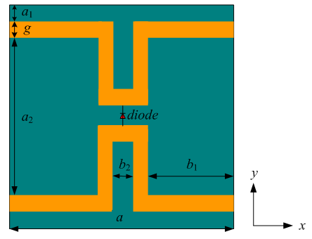
Figure 1. Front view of the meander-line absorber
To demonstrate the microwave absorption properties of our design, a full wave electromagnetic simulation has been performed based on the standard finite-difference time domain (FDTD) method by CST Microwave Studio software. For a plane wave normal incidence with the electric field parallel to the y-axis, no transmission has been examined, as it is blocked off by the metal film. Frequency characteristic of the absorption can be calculated using A(ω)=1-|S11|2. Fig. 2(a) shows the reflectivity magnitude S11 over the frequency range of 0.2–0.6 THz, where the dotted, dot-dashed, dashed, and solid lines mark values R=200, 350, 800 and 1500 Ω, respectively. The corresponding absorption is given in Fig. 2(b). For R=200 Ω, the structure has a small refection and the smallest reflection magnitude is 0.25 at 0.45 THz. As R increases to 350 Ω, the reflectivity level reduces to 0.05 at 0.42 THz. Increasing resistors from 800 to 1500 Ω makes reflection stronger with the central frequency has little change. In Fig.2 (b), the maximum absorption values at 0.42THz are 1, 0.89 and 0.67 for R=350, 500 and 1500 Ω, respectively, and the relative absorption bandwidth over 90% reaches to 15% for R=350 Ω.
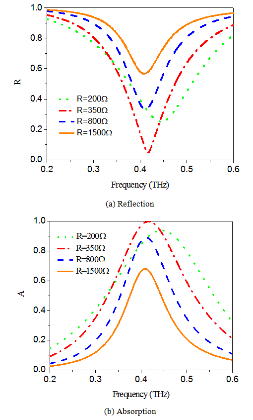
Figure 2. Simulated reflectance and absorption under different resistors
To clarify the mechanism underlying operation of the tunable absorber, the transmission-line equivalent circuit of the structure is shown in Fig. 3 [26, 27]. In this model, the metal lines are equivalent to be inductance L, the dielectric gap between metallic surfaces is equivalent to be capacitance C, ohmic losses can be taken into account by an additional resistor Ro, and the diode is modeled as a variable resistor Rs to represent the impedance of diode for varying bias voltage. Then, as the resistors changes, the whole impedance of the absorber can be varied in response to an applied electrical signal, the absorption of the basic unit will experience a high or low variation correspondingly. Furthermore, according to the equivalent circuit method, the resonant frequency ωo is dependent on the effective capacitance C and inductance L, i.e., ω0 ∝ (LC)-1/2. Then, the absorption frequency has little change with varying bias voltage.
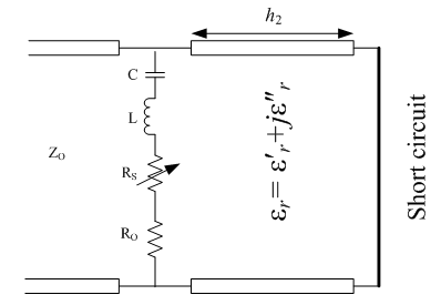
Figure 3. Transmission line equivalent circuit of the active absorber
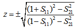
On the other hand, to better understand the mechanism of the high absorption, the relative impedance z can be retrieved from the simulated S parameters [28, 29], where
(1)
Fig. 4 shows the real part and imagery part of the relative impedances, where the dotted, dot-dashed, dashed, and solid lines mark values R=200, 350, 800 and 1500 Ω, respectively. At the absorbance peak frequency of 0.42 THz, the real parts of the relative impedances are 0.63, 0.99, 0.99 and 0.73, and the imagery parts are 0.4, 0.09, -0.68 and -1.17 for R=200, 350, 800, and 1500Ω, respectively. It is clear that the calculated relative impedance is more close to 1 for R=350Ω, which means the absorber achieves near perfect impedance matched to the free space.
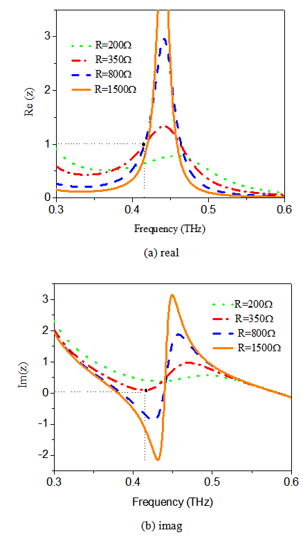
Figure 4. The real and imaginary parts of the relative wave impedances under different resistors
Fig. 5 shows the absorptions as a function of dielectric material for R=350Ω. The dot-dashed, solid and dashed lines represent εr=3, 3.9 and 5, respectively. As dielectric constant increases, the absorption peak shifts to the lower frequency with bandwidth decreasing. The effect of dielectric material on absorption frequencies can be explained from the equivalent circuit model. In fact, the resonant frequency ω0 is inversely proportional to the effective capacitance C and inductance L, i.e., ω0 ∝ (LC)-1/2, and C is directly proportional to the dielectric constant εr of the dielectric material. As a result, the absorption frequency shifts to the lower frequency with increasing εr.
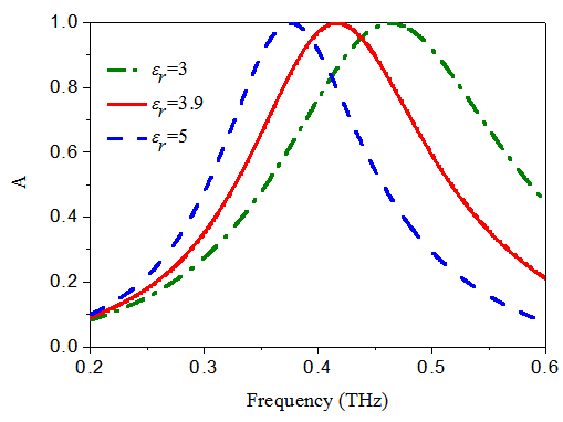
Figure 5. Absorption under different dielectric material

3. Conclusions

In conclusion, a tunable terahertz absorber based on voltage-controlled diodes is designed. The behavior of the active absorber can be described by the transmission-line equivalent circuit, in which, the reactance can be represented by a series combination of inductance and capacitance, and the diode is modeled as a variable resistor to represent the impedance of diode for varying bias voltages. By investing the real and imagery parts of the relative impedances under different resistors, it is found that the highest absorption is achieved when the relative impedance is more close to 1. When set the resistor to the largest absorption, the absorption frequency shifts to downward with increasing dielectric constant of dielectric material.

ACKNOWLEDGEMENTS

This work was supported by the National Natural Science Foundation of China under grant Nos. 11174280, 60990323, 60990320, and 61107030, and China Postdoctoral Science Foundation.

References

[1]  Federici, J. and Moeller, L., “Review of terahertz and subterahertz wireless communications”, J. Appl. Phys., vol. 107, pp. 111101-1-22, 2010.
[2]  Tonouchi, M., “Cutting-edge terahertz technology”, Nature, vol. 1, pp. 97–105, 2007.
[3]  Chen, H. T., Padilla, W. J., Zide, J. M. O., Gossard, A. C., Taylor, A. J. and Averitt, R. D., “Active terahertz metamaterial devices”, Nature, vol. 444, pp. 597-600, 2006.
[4]  Mittleman, D., “Metamaterials: A tunable terahertz response, Nature Photonics”, vol. 2, pp. 267–268, 2008.
[5]  Landy, N. I., Sajuyigbe, S., Mock, J. J., Smith, D. R. and Padilla, W. J., “Perfect Metamaterial Absorber”, Phys. Rev. Lett., vol. 100, pp. 207402-1-4, 2008.
[6]  Tao, H., Landy, N. I., Bingham, C. M., Zhang, X., Averitt, R. D. and Padilla, W. J., “A metamaterial absorber for the terahertz regime: Design, fabrication and characterization”, Optics Express, vol. 16, pp. 7181-7188, 2008.
[7]  Wen, Q. Y, Xie, Y. S., Zhang, H. W., Yang, Q. H., Li, Y. X., and Liu, Y. L., “Transmission line model and fields analysis of metamaterial absorber in the terahertz band”, Opt. Express, vol. 17, pp. 20256–20265, 2009.
[8]  Zhang, D. N., Wen, Q. Y., Xie, Y. S., “Simulation and experiments for a broadband terahertz absorber”, Chinese Optics letters, vol. 9, pp. S10402-1-3, 2011.
[9]  Huang, L., Chowdhury, D. Roy, Ramani, S., Reiten, M. T., Luo, S.-N., Taylor, A. J., and Chen, H.-T., “Experimental demonstration of terahertz metamaterial absorbers with a broad and flat high absorption band”, Optics Letters, vol. 37, pp. 154-156, 2012.
[10]  Ye, Y., Jin, Y., and He S., “Omni-directional, polarization-insensitive and broadband thin absorber in the terahertz regime”, J. Opt. Soc. Am. B, vol. 27, pp. 498-504, 2010.
[11]  Tao, H., Bingham, C. M., Strikwerda, A. C. et al., “High flexible wide angle of incidence terahertz metamaterial absorber: design, fabrication, and characterization”, Phys. Rev. B, vol. 78, pp. 241103R, 2008.
[12]  Tao, H., Bingham, C. M., Pilon, D., Fan, Kebin, Strikwerda, A. C., Shrekenhamer, D. Padilla, W. J., Zhang, X. and Averitt, R. D., “A dual band terahertz metamaterial absorber”, J. Phys. D: Appl. Phys., vol. 43, no. 22, pp. 225102-1-5, 2010.
[13]  Wen, Q. Y., Zhang, H. W., Xie, Y. S., Yang, Q. H., and Liu, Y. L., “Dual Band Terahertz Metamaterial Absorber: Design, fabrication, and characterization”, Appl. Phys. Lett., vol. 95, no. 24, pp. 241111-1-3, 2009.
[14]  Ma, Y., Chen, Q., Grant, J., Saha, S. C., Khalid, A. and Cumming, D. R. S., “A terahertz polarization insensitive dual band metamaterial absorber”, Optics Letters, vol. 36, no. 6, pp. 945-947, 2011.
[15]  He, X., Wang, Y., Wang, J., et al, “Dual-band terahertz metamaterial absorber with polarization insensitivity and wide incident angle”, Progress In Electromagnetics Research, vol. 115, pp. 381-397, 2011.
[16]  Gu, C., Qu, S.B, Pei, Z. B., Xu, Z., Liu, J. and Gu, W., “Multiband terahertz metamaterial absorber”, Chin. Phys. B, vol. 20, no. 1, pp. 017801-1-5, 2011.
[17]  Landy, N. I., Bingham, C. M., Tyler, T., Jokerst, N., Smith D. R., and Padilla, W. J., “Design, theory, and measurement of a polarization-insensitive absorber for terahertz imaging”, Phys. Rev. B, vol. 79, no. 12, pp. 125104-1-6, 2009.
[18]  Grant, J., Ma, Y., Saha, S., Lok, L. B., Khalid, A., and Cumming, D. R. S., “Polarization insensitive terahertz metamaterial absorber”, Optics Letters, vol. 36, no. 8, pp. 1524-1526, 2011.
[19]  Kong, H., Li, G. F., Jin, Z. M., Ma, G. H., Zhang, Z. W. and Zhang, C. L., “Polarization-independent Metamaterial Absorber for Terahertz Frequency”, J Infrared Milli. Terahz Waves, vol. 33, pp. 649–656, 2012.
[20]  Zhou, H., Ding, F., Jin, Y. and He, S. L., “Terahertz Metamaterial Modulators based on Absorber”, Progress In Electromagnetics Research, vol. 119, pp. 449-460, 2011.
[21]  Tennant, A. and Chambers, B., “A Single-Layer Tuneable Microwave Absorber Using an Active FSS”, IEEE Microwave and wireless components letters, vol. 14, no. 1, pp. 46-47, 2004.
[22]  Zhu, B., Feng, Y. J., Zhao, J. M., Huang, C. and Jiang, T. A., “Switchable metamaterial reflector/absorber for different polarized electromagnetic waves”, Appl. Phys. Lett., vol. 97, no. 5, pp. 051906-1-3, 2010.
[23]  Zhao, J., Cheng, Q., Chen, J., Qi, M. Q., Jiang, W. X. and Cui, T. J., “A tunable metamaterial absorber using varactor diodes”, New Journal of Physics, vol. 15, pp. 043049-1-12, 2013.
[24]  Yang, Y. J., Huang, Y. J., Wen, G. J., Zhong, J. P., Sun, H. B. and Oghenemuero, G., “Tunable broadband metamaterial absorber consisting of ferrite slabs and a copper wire”, Chin. Phys. B, vol. 21, pp. 038501-1-5, 2012.
[25]  Wen, Q. Y., Zhang, H. W., Yang, Q. H., Chen, Z., Zhao, B. H., Yang, L. and Jing, Y. L., “Perfect Metamaterial Absorbers in Microwave and Terahertz Bands”,http://cdn.intechopen.com/pdfs-wm/37018.pdf, 2012.
[26]  Costa, F., Genovesi, S., Monorchio, A. and Manara, G., “A circuit-based model for the interpretation of perfect metamaterial absorber”, IEEE Trans. Antennas Propag., vol. 61, no. 3, pp. 1201- 1209, 2013.
[27]  Luukkonen, O., Simovski, C., Granet, G., Goussetis, G., Lioubtchenko, D., Raisanen, A.V. and Tretyakov, S. A., “Simple and Accurate Analytical Model of Planar Grids and High-Impedance Surfaces Comprising Metal Strips or Patches”, IEEE Transactions on Antennas and Propagation, vol. 56, no. 6, pp. 1624-1632, 2008.
[28]  Chen, X. D., Grzegorczyk, T. M., Wu, B. I., J. Pacheco Jr. and Kong, J. A., “Robust method to retrieve the constitutive effective parameters of metamateria”, Phys. Rev. E, vol. 70, pp. 016608-1-7, 2004.
[29]  Smith, D. R., Vier, D. C., Koschny, T. and Soukoulis, C. M., “Electromagnetic parameter retrieval from inhomogeneous metamaterials”, Phys. Rev. E. vol. 71, pp. 036617-1-11, 2005.