-
Paper Information
- Previous Paper
- Paper Submission
-
Journal Information
- About This Journal
- Editorial Board
- Current Issue
- Archive
- Author Guidelines
- Contact Us
International Journal of Electromagnetics and Applications
p-ISSN: 2168-5037 e-ISSN: 2168-5045
2013; 3(4): 103-119
doi:10.5923/j.ijea.20130304.06
Miniaturized Dual-Fractal Antenna Structure for RFID Tags
 Abstract
 Reference
 Full-Text PDF
 Full-text HTML
1Department of Electronic and Communications Engineering, College of Engineering, Alnahrain University, Baghdad, Iraq
2Department of Computer Engineering, College of Engineering, Alnahrain University, Baghdad, Iraq
Correspondence to: R. S. Fyath, Department of Computer Engineering, College of Engineering, Alnahrain University, Baghdad, Iraq.
| Email: |  |
Copyright © 2012 Scientific & Academic Publishing. All Rights Reserved.
A design approach for the miniaturization of a dual-antenna structure (DAS) for radio-frequency identification (RFID) tag system is presented. The structure contains two radiating elements, one as a receiving antenna and the other as backscattering antenna, printed on the opposite sides of the substrate and perpendicular to each other to keep relatively lower coupling between them. The proposed design procedure contains number of intermediate steps, each of which produces antenna miniaturization as well as the desired impedance matching properties. The DAS is optimized using two softwares coupling to each other: a general computing tool (MATLAB) to implement the particle swarm optimization (PSO) technique and Electromagnetic Simulator (CST Microwave Studio) to extract antenna performance parameters. The aim of the optimization technique is to miniaturize the DAS under two strict conditions, namely maximizing both the feeding power to the IC tag connected to the receiving antenna (conjugate matching) and the backscattered fields difference (making the input impedance of the backscattering antenna pure real). The design approach is applied to both conventional and 3rd-order Sierpinski gasket, with ellipse generation, fractal bow-tie patch antennas and yields 49% and 68% area reduction, respectively, compared with the reference (non-fractal) single-antenna tag counterpart at 5.8 GHz band.
Keywords: Bow-tie antenna, Dual-fractal antenna structure, RFID antenna, Particle swarm optimization (PSO)
Cite this paper: D. K. Naji, R. S. Fyath, Miniaturized Dual-Fractal Antenna Structure for RFID Tags, International Journal of Electromagnetics and Applications, Vol. 3 No. 4, 2013, pp. 103-119. doi: 10.5923/j.ijea.20130304.06.
Article Outline
1. Introduction
- Radio frequency identification (RFID) has emerged as one of the most popular methods for asset, person, and object identification through the use of active or passive chipped tag antennas bearing a univocal identification code[1, 2]. In recent years, there has been rapid growth in the development of RFID systems for various applications including industrial fields[3-5]. An RFID system is comprised of tags, readers, and information management system. In developing an RFID solution, the focus is usually placed on designing high performance tags suitable for practical applications[6]. The tag's antenna has to be small in size and light in weight, as it is attached to the objet that would be identified, and should be also inexpensive for mass production[7]. However, the design of RFID tag antennas is a tradeoff between size reduction and performance[8-10].For most RFID applications, it is strongly desired to maintain a minimal fast print for the tag. Therefore, passive tags attract increasing interest in RFID applications[11, 12]. The fundamental idea of passive RFID system is that the transponder is powered via the air interface by means of magnetic fields or electromagnetic radio waves and hence the system can operate without the use of any external energy storage devices[13, 14]. A typical passive tag consists of an antenna and an application specific integrated circuit (ASIC) chip. The communication between the reader and the passive tag involves two links[15]i) Forward link: The reader sends out continuous wave (CW) and commands to the tag. The tag chip turns on and responds to the command when it receives sufficient power from the CW.ii) Backward link: The tag antenna is alternatively connected to two different load impedances according to the data stored in the chip. The CW is modulated in this manner and scattered back to the reader.To achieve successful communication between the reader and the tag, two conditions must be satisfied simultaneously. First, conjugate impedance matching between the tag antenna and the chip must be exists to ensure maximum power transfer to power the chip. Secondly, the difference between the high and low levels of the backscattered wave is large enough to enable the reader to demodulate the backscattered signal correctly.Conventional passive tag RFID systems have one antenna to serve as receiving antenna and backscattering antenna[16, 17]. A single antenna cannot be designed optimally to meet the above two conditions at the same time because the design requirements are different. Recently, Chen et al.[15] have reported a pioneer work describing a proposal for a dual-antenna structure (DAS) to be used in UHF RFID tags. One of the antennas is for receiving and designed to have the maximum power transfer to the tag chip, while the other is for backscattering and designed for the maximum differential backscattering. The concepts are verified experimentally at 915 MHz using two linearly tapered meander dipoles printed on the opposite sides of the substrate. It is worth to mention here that the issue of antenna miniaturization was not discussed by the authors in[15]. The work reported in this paper uses the main concepts reported in[15] to design a miniaturized DAS for 5.8GHz RFID tags. The miniaturization is based on particle swarm optimization (PSO) technique which is applied for both conventional DAS and its fractal counterpart. The fractal geometry is introduced in the structure to achieve further miniaturization. In fact, the electrodynamical properties of fractal geometries have been extensively studied by several authors focusing on their multiband behavior and ability to operate as efficient small antennas. As a matter of fact, the use of fractal geometries for antenna design has been proven to be very effective in achieving miniaturized dimensions and an enhanced bandwidth, even though a reduction of the radiation efficiency at resonance frequencies takes place[18]. Fractal geometry which is suitable for antenna design is infinite and there must be better shape candidates among those geometries for antennas. Therefore, design and fabricating of fractal geometry is the premier topic of research of fractal antenna. The design issues reported in this paper takes the bow-tie antenna (BTA) as a reference one. It is well known that BTAs are a planar form of ultra-wideband finite biconical antennas. It is a practical angle-dependent frequency independent antenna[19]. Because of its ultra-broadband, light weight, thin profile configurations, low cost, and easiness of fabrication, reliability and conformability, BTAs have been widely studied and used in engineering applications. Also, the simple geometries make it compatible to be connected to planar feeding system in an integrated architecture. In this paper, a modified Sierpinski gasket fractal geometry with ellipse generation is designed and introduced into the typical bow-tie antenna.The goal of this paper is to introduce optimization based-approach for miniaturizing DAS for RFID tag systems. One of the main advantages of this approach is its ability to generate automatically the shape of the antenna according to both the geometric antenna parameters constraints and required optimization fitness function. The steps followed to design a miniaturized DAS are introduced and investigated in detail. The impedance matching and radiation characteristics of the optimized conventional and fractal BTA-based DASs are presented and discussed for 5.8GHz operation.
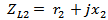
2. Concepts of Dual-Antenna Structure
- In a conventional loaded antenna (such as RFID tag), the scattered field can be considered from either load-dependent component (associated with re-radiated power from the match-loaded antenna) or load-independent components (associated with scattering from the open- or short-circuited antenna)[20]. For minimum scattering antenna this power can be calculated from the antenna equivalent circuit of Fig. 1a (where
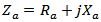 is the antenna input impedance and
  is the antenna load). The load
  takes one of the following modes:(i) Backscattering mode●
 corresponding to open-circuited load state.●
 corresponding to short-circuited load state.(ii) Receiving mode●
 corresponding to the complex input impedance of the chip.The complex reflection coefficient at the load is given by
 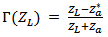 | (1) |
 ,
,  and
and  (perfect matching), yields
 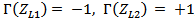 , and
, and  . The difference of the two scattering levels,
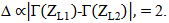
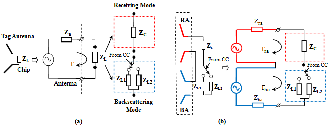 | Figure 1. RFID tag and its equivalent circuit. (a) Conventional. (b) Dual-antenna structure (DAS). RA= Receiving Antenna, BA=Backscattering Antenna, CC= Control Circuit |
 should be conjugate matched to the input impedance of the chip,
  (i.e.,
  ) to ensure maximum power transfer to the chip (i.e., the receiving antenna reflection coefficient
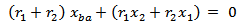
  ). The backscattering antenna operates with two different load states, namely very high-impedance load ZL1 when the switch is OFF and very low-impedance load ZL2 when the switch is ON. The control circuit (CC) within the chip is responsible for switching the impedance states according to the data stored. The difference in the scattered field strength between the two states
  is proportional to
  , where
  is the backscattering reflection coefficient. The parameter
  should be maximized to enable the reading antenna to simply differentiate between the high level and low level of the backscattered signals modulated in accordance with the data stored in the tag chip. This condition is best satisfied when
  for any argument
  [15].The condition
  reveals that
 | (2) |
 | (3) |
 | (4a) |
 | (4b) |
 | (4c) |
 | (5a) |
 | (5b) |
 | (6) |
 | (7) |

 .For ideal switching states (i.e.,
 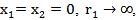 and
and  eqn. (7) gives
  and predicts a finite value for
  . Under this environment,
  and
and  which offer the maximum allowable value of
  .
.3. Design of Bow-Tie Antenna
- Figure 2 shows detailed design geometry of a BTA which will be used as a reference structure to optimize both the receiving and backscattering antennas for conventional and dual-antenna structure. Initially, the antenna is designed using a set of equations and then the results are fine-tuned using CST software to achieve the required resonance frequency. The used design equations are[21]
 | (8a) |
 | (8b) |
 | (8c) |
 | (8d) |
 | (8e) |
 is the resonance frequency and the substrate is characterized by three parameters
  and
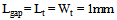
and  which denote its thickness, relative and effective permittivity, respectively. Other geometric parameters appeared in these equations are defined in Fig. 2.The reference BTA is designed to resonate at 5.8 GHz using a substrate having h = 1.6 mm and
  (FR4). The initial design starts with the assumption that each side of the BTA is approximated by an equilateral triangle (i.e.,
  and Wp
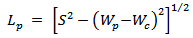
  Wc). From antenna basic theory, the effective length of the antenna "S" should be approximately equal to
  where
where  is the resonance wavelength and
  is the speed of light in free space.The initial design takes Wp =
  = 12.93 mm and
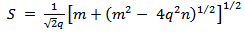
  . Equation (8d) predicts an effective permittivity
  of 3.48 (which is less than
  ) and accordingly eqn. (8c) gives
  mm. Afterwards, the value of the geometric parameter S can be computed by combining eqns. (8a) and (8b) to get the following equation
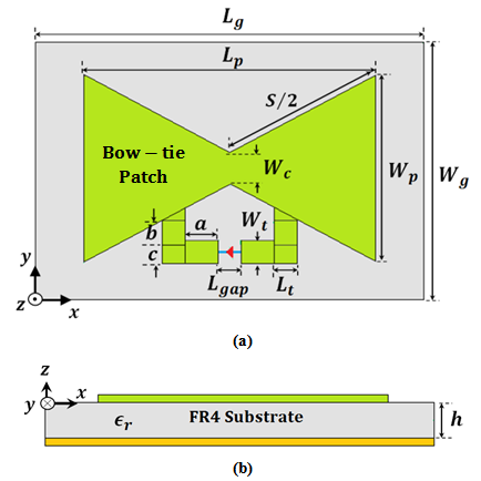 | Figure 2. Geometry of the bow-tie patch including matching loop. (a) Front view. (b) Bottom view |
 | (9) |
 | (10a) |
 | (10b) |
 | (11) |
 | (12) |
 | (13a) |
 | (13a) |
 is shifted from 5.66 GHz (theoretical) in the initial design to 5.80 GHz (simulation) in the finalized design.
|


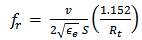
4. Design Optimization Approach
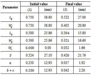
- An optimal approach for exploiting miniaturization and matching properties of DAS for RFID tag systems is based on introducing dependent and independent geometric parameters. This to ensure more degrees of freedom for antenna design, avoid the generation of unrealizable structures, and prevent the occurrence of failure in optimization process. Accordingly, to comply with electrical and geometric constraints by properly defining the geometric parameters of the radiating antenna structure (bow-tie with matching loop), the design procedure can be considered as an optimization problem. In the following subsection, a detailed optimization design approach and the performances of the miniaturized single- and dual-antenna structures for RFID tags are presented. Figure 3 illustrates the geometry of the proposed dual-bow-tie antenna with its matching loop. The structure consists of both receiving and backscattering antennas. The two antennas are printed on opposite sides of the structure and perpendicular with each other to reduce coupling between them.
 | Figure 3. Proposed dual-antenna geometry. (a) 3D configuration. (b) Front side. (c) Bottom side. (d) Back side |
4.1. Conventional Backscattering Antenna
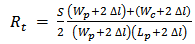
- In this subsection, the designs of miniaturized backscattering antennas (MBAs) for different desired real input impedances are presented. The main goal of this design is to investigate the dependence of the miniaturized area on the input antenna impedance. Different desired input impedances,
 (50, 100, 150, 200, 250 and 500Ω) are chosen for designing a backscattering antenna with miniaturized area. The geometry of the backscattering antenna is the same as that in Fig. 2, but with replacing its front side by its back side (i.e., bow-tie patch printed in the back side substrate). Additional subscript 2 is added to the symbols to define bow-tie and matching loop geometry parameters for this antenna.Eight antenna geometric parameters enter the optimization process, one is considered as independent parameter, ground length
  , and the other seven are considered as dependent parameters. Equation (14) describes the relation among dependent and independent geometric parameters
  | (14a) |
 | (14b) |
 | (14c) |
 | (14d) |
 | (14e) |
 | (14f) |
 | (14g) |
 and
and  , represent, scaling parameters for generation the corresponding parameters, ground length
  , patch length
  , patch width
  , and
, and  respectively. Whereas, in eqns. (14e)-(14g),
  ,
,  , and
, and  denote the scaling parameters that responsible for matching loop parameters generation
  , and
, and  , respectively.The following optimization fitness function is used to miniaturize this antenna for different values of
  .
.  | (15a) |
 | (15b) |
 | (15c) |

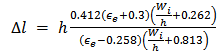
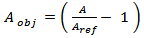
 Note that the optimization fitness function, eqn. (15a) consists of two objective functions
  and
and  which are related to complex return loss and antenna area, respectively. In eqn. (15b),
  and
and  represent, respectively, the actual and desired values of backscattering reflection coefficient at resonance frequency, and
  is the unit step function. In eqns. (15b) and (15c),
  and
and  represent, respectively, the area of the reference and the optimized antennas. Also,
  and
and  are the lower and upper bounds on the
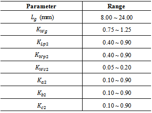
  design variables, respectively. The PSO algorithm adopted here is a basic one follows closely with that in Ref.[22]. The number of PSO particles required to perform the optimization are 24 particles, three for each one of the eight parameters that entered the optimization. A stop criterion is chosen such that 60 PSO iterations are reached or the fitness function remains unchanged with less than 2% error for at least 20 successive iterations. The constraints used in the optimization process for the geometric parameters of the backscattering antennas are listed in Table 2.
|
|
 (50, 100, 150, 200, 250 and 500Ω) at
  = 5.8 GHz
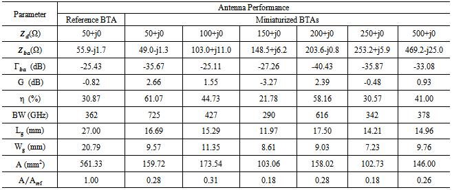
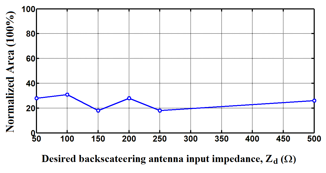 | Figure 4. Normalized area versus the desired backscattering input impedance, |
 . One can see from Table 3 and Fig. 4 that a normalized area of 18%-28% is achieved for these antennas, i.e., antenna areas of 102 - 173 mm2, for.
  . Also, It seen from Table 3 that the miniaturized BA for
  gives good performance (gain of 2.66 dB, efficiency
  and bandwidth
  ) compared with other antennas of
  . Thus,
  is used as the desired real-valued input impedance for the backscattering antenna during the optimization of the DAS in the following subsections.Figure 5 depicts the return loss and input impedance of the miniaturized backscattering antenna for
  . One can conclude from this figure that complex return loss of -38.44 dB with input resistance and reactance of 49.27
 and -0.94
 , respectively, at 5.8 GHz resonance frequency are achieved. The 3D radiation pattern of this antenna is shown in Fig. 6. It is noticed from this figure that maximum radiation pattern is in the broadside direction of the patch and minimum or approximately no radiation behind the backside (ground plane).
 | Figure 5. Return loss (a), input, resistance (b), and input reactance (c) of the miniaturized BA with  |
 | Figure 6. 3D radiation pattern (gain) of the miniaturized BA with  . Note that (-z and –x) coordinates are used here to see clearly the radiation . Note that (-z and –x) coordinates are used here to see clearly the radiation |
4.2. Conventional Receiving Antenna
- In this subsection, the receiving antenna is optimized in the same manner that mentioned in previous subsection, but for conjugate impedance matching
 . The structure of this antenna is the same as that of Fig. 2. An additional subscript 1 is added to the symbols of geometric parameters of the bow-tie patch-shape and matching loop structure. The optimization fitness function, eqn. (15a), is used for miniaturizing this antenna with the receiving antenna return loss
  defined in eqn. (1) for
  . The antenna is optimized for
  at resonance frequency
  . The used geometric parameters, ranges of constraints, and number of particles are as in the previous subsection.The return loss and the corresponding input resistance and reactance of the miniaturized receiving antenna (MRA) are shown in Fig. 7. It is shown from this figure that good conjugate matching with complex load
 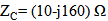 is achieved at
  . Return loss less than -39 dB and input impedance
  at 5.8 GHz are obtained. The 3D radiation pattern of MRA is shown in Fig. 8. Note that more radiation is in the front of the patch and less radiation in its back side.Table 4 lists the optimized geometric parameters for the receiving, backscattering, and the reference antennas. The corresponding performance parameters are given in Table 5. The following findings can be drawn from these two tables:i) Return loss less than -25 dB at the resonance frequency 5.8 GHz is achieved for all antennas.ii) Miniaturized backscattering antenna has the greatest gain and bandwidth (2.66 dB and 720 MHz) while the receiving antenna has the lowest gain and bandwidth (-3.99 dB and 240 MHz).iii) The receiving antenna offers higher reduction of area
  , (81%) compared with backscattering antenna (71%)
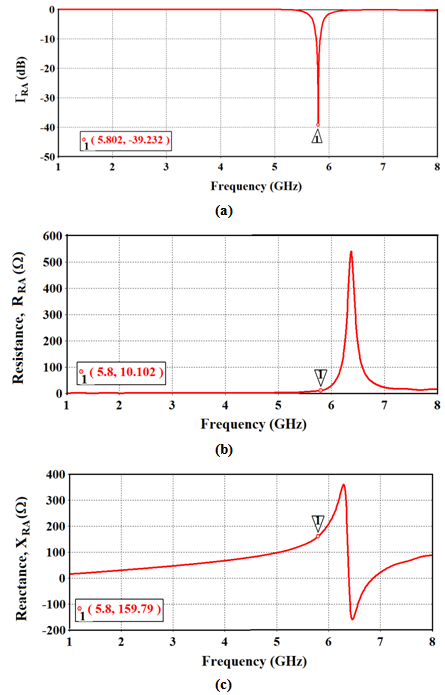 | Figure 7. Return loss (a), input resistance (b), and input reactance (c) of the miniaturized RA for  |
 | Figure 8. 3D radiation pattern (gain) of the MRA for  |
|
 . Rsesults corresponding to the reference antenna are also included for comparision purposes
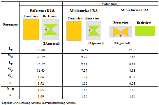
|
 . Rsesults corresponding to the reference antenna are also included for comparision purposes
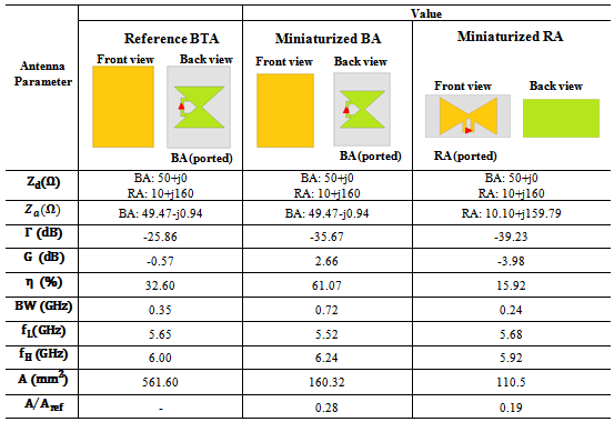
4.3. Dual-Antenna Structure
- In the previous subsections, the performance of conventional antenna structure for receiving and backscattering sides are designed and investigated in detail. In this subsection, the DAS presented in Fig. 3 is designed and investigated. In this design, the proposed antenna is printed on a 1.6-mm thick FR4 substrate of varying size
 mm3 comprising a radiating portions (bow-tie shape and matching loop) at both of its side. The dimensions of the radiating portion and matching loop of the receiving antenna are denoted by
  and
and  , respectively. For the scattering antenna, the dimensions of the radiation portion and matching loop are denoted by
  and
and  , respectively. The fitness function used to miniaturize this antenna is the same as that in eqn. (15), but the return loss objective function consists of two terms rather than one term. Thus, eqn. (15) is rewritten as
 | (16a) |
 | (16b) |
 | (16c) |
 | (16d) |

 where
where  and
and  represent the complex return loss of backscattering and receiving antennas at the resonance frequency
  , respectively. The goal of this fitness function is to miniaturize the overall area (Lg x Wg) of this DAS subject to keeping both the return losses
  and
and  below the desired value
  at the required resonance frequency
  .The geometric parameters enter the optimization process are fourteen, two for the common ground,
  and
and  , and six for the receiving (backscattering) bow-tie shapes,
 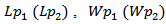 and
and  , and six for matching loop geometries
 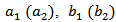 and
and  . The number of particles used to optimize this antenna is 42, three for each of the 14 geometric parameters that enter the optimization process.
 5. Performance of the Dual-Antenna Structure
- The proposed DAS is optimized to operate as receiving and backscattering antennas at the center frequency 5.8 GHz. The receiving antenna is to be conjugate matched to
 while the backscattering antenna having a
  input impedance. In this section, the performance of this proposed antenna is presented and discussed for three cases:Case 1: Both RA and BA are connected to a 50Ω-port or both antennas are under test (AUT).Case 2: The RA is AUT and BA is connected to an open- or a short-circuited load.Case 3: The BA is AUT and the RA is connected to a conjugate matched load.
5.1. Performance of RA When BA Being Open- or Short- Circuited (Case 2)
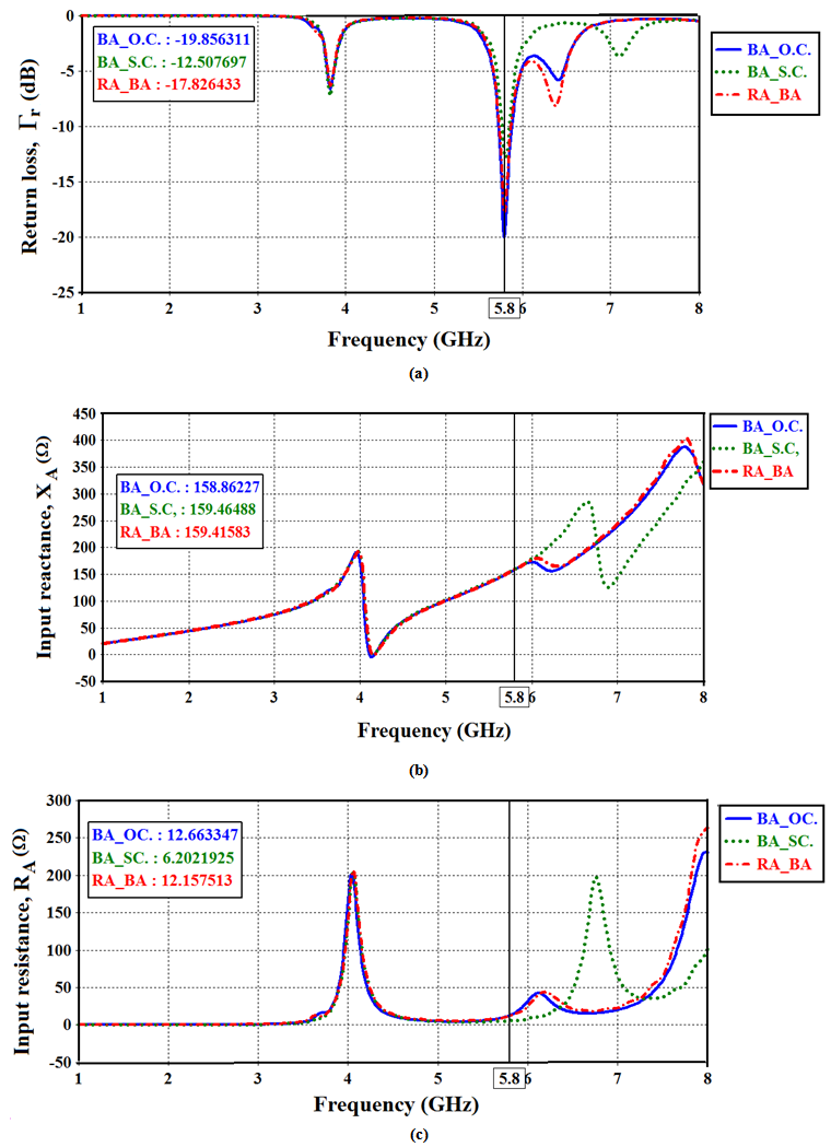
- This subsection addresses the performance of the receiving antenna when the backscattering antenna being short- or open- circuited. Before doing this, the isolation coupling between RA and BA must be studied first since it's the most factors affecting the antenna performance. Figure 9 shows the isolation coefficient response for the proposed DAS. A coupling less than -17dB is obtained for frequencies less than 6 GHz, with less than -20 dB at 5.8 GHz. Thus, due to such low coupling, the receiving antenna is unaffected by shortening or opening the backscattering antenna. Also, the backscattering antenna is not affected by introducing the matching receiving antenna. Therefore, it is a good result to resume the simulation and address the performance of the proposed antenna.Figure 10 shows the return loss and real and imaginary parts of the input impedance against frequency. It is seen from this figure that when the backscattering antenna is short circuited (BA_SC) or open circuited (BA_OC), nearly no changes occur in the return loss and input impedance of the receiving antenna beyond 5.8 GHz. In contrast, above 5.8 GHz, changes in return loss and impedance occur for the BA_SC while no changes in performance are obtained for the BA_OC. In addition, minimum changes are found for the imaginary part of input impedance of RA at 5.8 GHz for both cases, BA_SC or BA_O.C. Whereas more variation occur for the real part of input impedance of the RA at 5.8 GHz, +2.66
 and -3.80
 with respect to 10
 , real part of the load
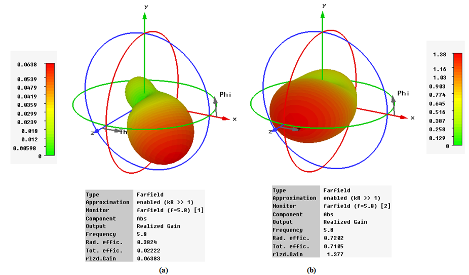
  .Figures 11(a) and 11(b) show the 3D gain pattern of the receiving and backscattering antennas, respectively. One can noticed from this figure that both antennas radiate in the front side of the dual-antenna structure
 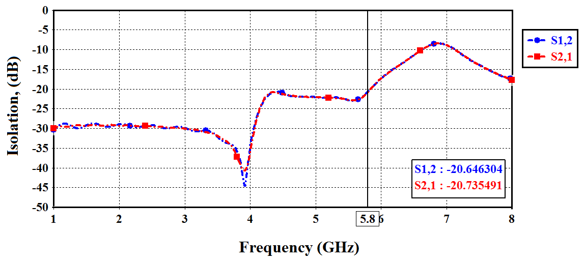 | Figure 9. Isolation between receiving and backscattering antennas |
 | Figure 10. Return loss (a), input resistance (b), and input reactance (c) of the DAS when BA is open circuited (BA_OC) or short circuited (BA_SC), and when RA and BA are ported (RA_BA).  , and , and  |
 | Figure 11. 3D radiation pattern (gain) of the dual-antenna structure at 5.8 GHz when both RA and BA are under test. (a) RA. (b) BA |
 | Figure 12. Return loss (a), input resistance (b), and input reactance (c) of the dual-antenna structure when RA is matched load (RA_ML), and when RA and BA are ported (RA_BA).  and and  |
5.2. Performance of BA When RA Being Conjugate Matched (Case 3)
- In this subsection, the performance of the backscattering antenna is investigated when the receiving antenna is matched to the load
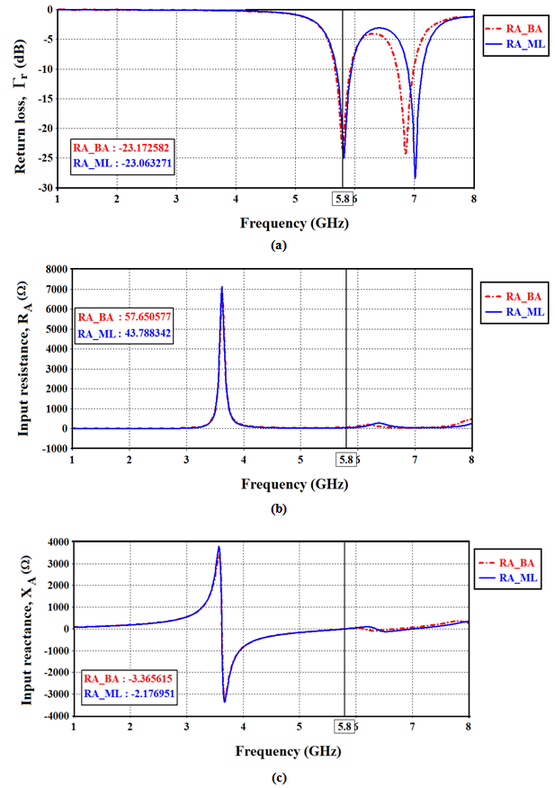
 . Figure 12 shows the complex return loss and input impedance of the backscattering antenna which is AUT and the receiving antenna is connected to a matched load (case 3).Investigating this figure reveals that the return loss and input impedance of the backscattering antenna are not affected by connecting a matched load to the receiving antenna. Table 6 lists a summary of the antenna performance for the aforementioned two cases beside case 1 (both antennas, RA and BA are AUT).
6. Dual-Fractal Antenna Structure
6.1. Modified Sierpinski Fractal Geometry
- A fractal BTA (FBTA) is introduced here to miniaturize further the DAS for RFID tag applications at 5.8 GHz. The fractal geometry is embedded in both receiving and backscattering antennas. Figure (13) shows the first three fractal orders of the proposed FBTA. The fractal geometry used here is an extended version of the modified Sierpinski gasket adopted in[23]. The extension is based on ellipse fractal finger print rather than circle that used in[23]. The reason behind this modification is that the ellipse structure is characterized by higher degree of freedom which is required to enhance the filling factor of the fractal antenna and therefore more miniaturization will be achieved. The first -order fractal geometry shown in Fig. (13b) is constructed by subtracting a central ellipse I with radii
 and
and  of 1/3-scaled of patch width (Wp) and halved-value patch length (Lp) of the main triangular shape. Three equal ellipses 1, 2, and 3, each one being (1/3) of the size of the ellipse I and placed at (Lp/16, Wp/2), (Lp/8, ±Wp/4), respectively, are subtracted from first fractal order geometry to produce second-order fractal, Fig. (13c). One can iterate the same subtraction procedure to generate a third-order structure by subtracting nine equal ellipses, each one being (1/3) of the size of the ellipses 1, 2 or 3, Fig. (13d). Equation (17) describes the geometrical parameters generation and their dependence on BTA parameters
  | (17a) |
 | (17b) |
 | (17c) |
 | (17d) |
 and
and  of one-third and one-sixth of patch width Wp and patch length Lp, respectively. In the same manner, the second-order fractal is generated by subtracting six ellipses located at distances
  and
and  with respect to Wp and Lp, respectively, each one of one-third of the main ellipse, from the first-order fractal as shown in Fig. (13c). The third-order fractal is generated in the same procedure as shown in Fig. (13d).In this work, a 3rd-order FBTA is miniaturized at 5.8 GHz to maximize the feeding power to the IC tag connected to the receiving antenna (conjugate matching with a chip having an input impedance of
  and to make the input impedance of the backscattering antenna pure real (50Ω) for maximum backscattered field difference.
6.2. Performance of a 3rd-order FBTA
|
 = 5.8 GHz for the three operating cases
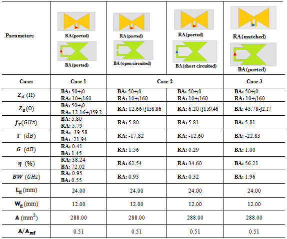
|
 = 5.8 GHz
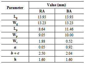
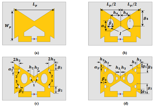 | Figure 13. Front side of the dual-antenna structure with Sierpinski fractal bow-tie geometry and ellipse generation. (a) Reference BTA. (b) First-order FBTA. (c) Second-order FBTA. (d) Third-order FBTA |
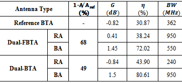
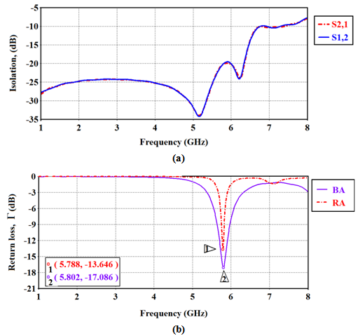
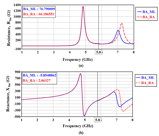
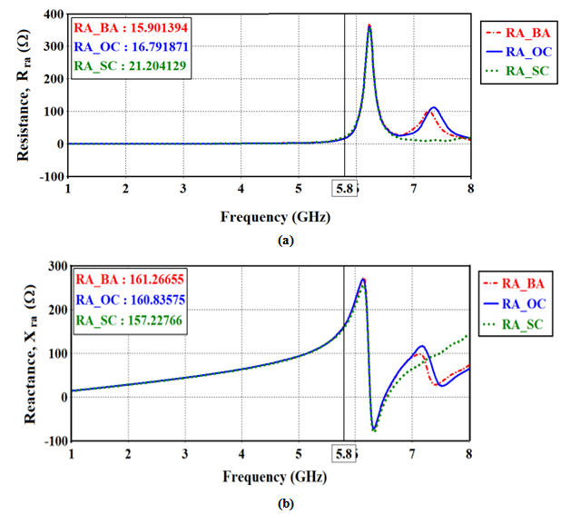
- The optimization fitness function described by eqn. (16), is used here with 14 geometric parameters whose ranges are given in Table 4. Tables 7 and 8 list the antenna geometric and performance parameters for the 3rd-order FBTA. Investigating Tables 7, 8, and 5 reveals the following findings which are listed in Table 9(i) Area reductions of 68% and 49% are achieved by the 3rd-oredr fractal and conventional BTA for DAS, respectively, with respect to single-structure reference BA.(ii) Bandwidth of (0.95 and 0.55 GHz) and (0.24 and 0.95 GHz) are obtained with the receiving and backscattering antennas by the fractal and non-fractal BTA, respectivelyFigure 14(a) and 14(b) show the isolation between receiving and backscattering antennas and the return losses of them. It is seen that more than 20 dB of isolation is achieved for frequencies less than 6.4 GHz, thus, good performance will be achieved for different operating conditions (cases 1-3). In Fig. 14(b), good matching of -12.63 and -17.07 dB are satisfied for the receiving and backscattering antennas at 5.8 GHz, respectively. Figures 15(a) and (b) depicts the resistance and reactance characteristics of the backscattering antenna when the receiving antenna is matched to a load of impedance 10-j160Ω. It is seen from this figure that a resistance of more than 60Ω and reactance less than -6Ω is achieved when the receiving antenna is ported to 50Ω or conjugate matched to the load. Figures 16(a) and (b) show the resistance and reactance of a receiving antenna when the backscattering antenna is connected to an open- or a short circuited load. Note that resistance between 15.90 Ω and 21.20 Ω, and reactance between 157.22 Ω and 161.26 Ω are obtained for the receiving antenna when the backscattering antenna is open- or short-circuited. Thus, good matching properties are achieved for both receiving and backscattering antennas irrespective of connecting load to a receiving antenna or making backscattering antenna short or open circuited.
|
 = 5.8 GHz. Both antennas RA and BA are excited by
  port
port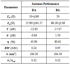
|
 | Figure 14. Isolation between the receiving and backscattering antennas (a) and return loss (b) of the fractal bow-tie antenna |
 | Figure 15. Input resistance (a) and input reactance (b) of the dual-fractal antenna structure when RA is matched load (RA_ML) and when RA and BA are ported (RA_BA).  and and  |
 | Figure 16. Input resistance (a) and input reactance (b) of the dual-fractal antenna structure when BA is open circuited (BA_OC) or short circuited (BA_SC), and when (RA and BA are ported (RA_BA).  , and , and  |
 | Figure 17. Reading ranges of the miniaturized antennas as a function of frequency |
 | (18) |
 is the wavelength,
  is the power transmitted by the reader,
  is the gain of the transmitting antenna,
  is the gain of the tag antenna. The times of
  by
by  is called ERIP (Equivalent Radiated Isotropic Power),
  is the minimum threshold power necessary to turn on the chip, and
  is the power transmission coefficient which is given by
 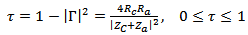 | (19) |
 represents the chip impedance
  and
and  represents the antenna impedance
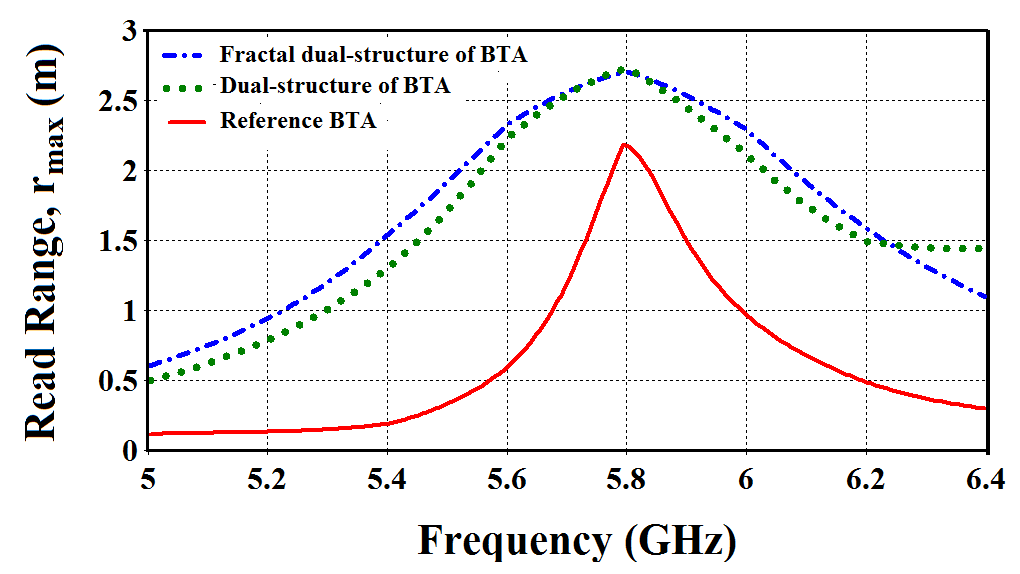
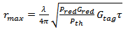
  . In addition, when maximum power is transferred the antenna is said to be perfectly matched to the chip impedance at a particular frequency.The reading ranges for each of the designed antennas, reference BTA and conventional and fractal dual-structure BTAs are calculated over the operating frequency range using eqn. (18). The results are displayed in Figure 17 for value of ERIP = 3.2 W and threshold power Pth = 10 μW. It can be observed that all RFID tags are functional across the entire ISM frequency band of 5.725–5.875 GHz. At 5.8 GHz, the reading ranges are 2.18, 2.7, and 2.7m for reference BTA, conventional and fractal dual-structure BTAs, respectively.
 7. Conclusions
- Dual-antenna structures (DASs) for 5.8 GHz RFID systems have been proposed and simulated using conventional and fractal bow-tie patch geometries. An optimization-based approach is introduced to miniaturize the proposed DAS which consists of two antennas, one is the receiving antenna at the upper side, and the other one is the backscattering antenna at the other side. Two objective functions are used to satisfy the design requirements of the proposed dual structure, one for conjugate matching the receiving antenna to the IC chip and to make the input impedance of the backscattering antenna pure real, and the other objective function is to minimize structure area. A compact size 3rd-order DAS structure is achieved from the optimization approach (13.93 X 13.23 mm2 or 0.27 X 0.25 λ2 at 5.8 GHz) Because of the low mutual coupling, the backscattering antenna performance is not affected by loading the receiving antenna. Also, the receiving antenna performance nearly does not change by loading the backscattering antenna by the two states of loading, short or open circuit.