-
Paper Information
- Previous Paper
- Paper Submission
-
Journal Information
- About This Journal
- Editorial Board
- Current Issue
- Archive
- Author Guidelines
- Contact Us
International Journal of Electromagnetics and Applications
p-ISSN: 2168-5037 e-ISSN: 2168-5045
2013; 3(4): 70-80
doi:10.5923/j.ijea.20130304.03
Performance Evaluation of Band-Notch Techniques for Printed Dual Band Monopole Antennas
 Abstract
 Reference
 Full-Text PDF
 Full-text HTML
Khalil H. Sayidmarie, Tariq A. Najm
Department of Communication Engineering, College of Electronic Engineering, University of Mosul, Mosul, Iraq
Correspondence to: Khalil H. Sayidmarie, Department of Communication Engineering, College of Electronic Engineering, University of Mosul, Mosul, Iraq.
| Email: |  |
Copyright © 2012 Scientific & Academic Publishing. All Rights Reserved.
Three methods for band-notching in printed monopole antennas are investigated. A dual band monopole antenna in the form of double rectangular rings is considered in the investigation. The antenna covers the frequency bands of the IEEE 802.11a/b/g standard (2.4-2.48GHz, 5.15-5.35GHz and 5.725-5.825GHz), while a notch in the frequency range of 4-5 GHz is implemented. The performances of each of the three band notching techniques against various parameters are shown. The overall performance of the band-notch techniques using; parasitic element, slots, and stubs are compared. The CST microwave software package has been used in the investigations.
Keywords: Band-notched Antennas, Dual Band Antennas, Planar Monopole Antennas, WLAN Antennas
Cite this paper: Khalil H. Sayidmarie, Tariq A. Najm, Performance Evaluation of Band-Notch Techniques for Printed Dual Band Monopole Antennas, International Journal of Electromagnetics and Applications, Vol. 3 No. 4, 2013, pp. 70-80. doi: 10.5923/j.ijea.20130304.03.
Article Outline
1. Introduction
- The rapid growth of modern wireless communication systems such as smart phones, GSM, UMTS, LTE, and WLAN has motivated the research into suitable antennas suitable for these systems. Many of the modern wireless devices can incorporate more than one system, operating at different frequencies or spanning a very wide bandwidth. However, over the desired operational bandwidth, there may be some narrow bands occupied by other co-existing wireless systems. These co-existing systems can cause interference, and hence their frequencies should be blocked by either a band-reject filter or by some other techniques. On the other hand, to minimize noise effects, a multiband antenna system is preferred to receive minimal signal at frequencies in-between bands. Another requirement for a band notching is to prevent sensitive components, within the front-end of the receiver, from being overloaded by strong signals. Instead of deploying more than one antenna in such wireless devices, multiband antennas have found extensive use in these devices. These antennas should offer filtering properties not only to remove the effect of interference but also to get rid of additional bandstop filters, that are required to reject signals at unwanted frequencies. Therefore, various antennas with single or multiple notch functions have been developed for UWB communication systems, and WLAN systems[1]-[8]. One of the main conventional techniques for achieving band-notch characteristics is the use of slots or slits of various shapes. The slots can be deployed in; the radiating patch[6, 9], the feed line[7, 8], or the ground plane[10, 11]. The slots or slits are made to resonate at the notch frequency, resulting in disturbance of the current distribution on the radiating element, or reduce matching with the feed line. An alternative approach is to introduce parasitic elements adjacent to the radiating patch[12-14] or the feed line[15, 16]. The parasitic elements are made to resonate at the notch frequency where maximum energy is coupled to them. Consequently, there will be disturbance in the current distribution across the radiating element. The parasitic element, when placed adjacent to the feed line, receives coupled energy when it resonates at the notch frequency, and thus changes the input impedance of the antenna. The third approach is to attach a stub either to the feed-line or to the radiating patch[17-18]. The stub is well known for its use in matching, however, it should be noted that in this paper, it is rather used to produce adequate mismatch at thenotch-frequency.A segmented structure was recently proposed as a versatile approach to reject certain band of UWB printed monopole antennas. The method was implemented on circular, beveled rectangular, and regular hexagonal shaped monopole antennas[19]. By segmenting the radiating patch into three parts, intensive coupling occurs between the fed segment at the center of antenna and the two parasitic side segments at the target frequency, and consequently the band-notched property is obtained. It is worthy to mention that such segmentation or chopped process has been recently proposed to enhance the phase response of reflectarray elements[20]. A compact planar monopole UWB antenna of a spade-shaped radiation patch with four tunable notched bands has been proposed in[21]. The antenna employs three crescent-shaped parasitic resonators on the back side and an inverted U-slot in the ground plane, thus employing two of the band-notch techniques simultaneously. Another example of using a slot in the radiating patch, and two parasitic open-rings adjacent to the ground plane has been presented in[22]. The parasitic elements have also been arranged in multilayer configuration as in[23] where four notched-bands have been achieved.In this paper, a compact monopole antenna consisting of dual rectangular rings, and a 50Ohm microstrip feed line is investigated for the implementation of various band-notch techniques. It should be emphasized that the results reported in this paper are generated using the CST software package which is used in the design and parametric studies of the investigated antennas. Three band-reject techniques are studied thoroughly, where the effect of various parameters on the performance are investigated. The study aims at comparing the performance and capability of the investigated techniques. The paper is arranged as the following. After an introductory section, the design of dual ring antenna, considered in the investigations, is presented. Sections 3 to 5 present results of investigating the three notch techniques. Section 6 gives comparison of the obtained results, while section 7 lists the conclusions.
2. Antenna Design
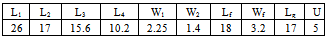
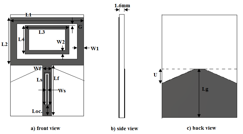
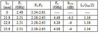
- The antenna considered in the investigation of the band notch techniques is a dual band monopole antenna presented recently in[24]. This antenna, which uses two concentric rectangular rings, deploys the self similarity property of the fractal geometry to implement dual-band operation. The dimensions of the two rings were initially chosen such that the mean circumference of each ring corresponds to the effective wavelength at the center of each of the wanted frequency bands. Thus the outer ring corresponds to the lower band while the inner ring corresponds to the upper band. The antenna is simulated using FR-4 substrate with a dielectric constant of 4.4, thickness of 1.6 mm, and a loss tangent of 0.025. The width of the feed line for each antenna was fixed at 3.2 mm to implement 50 Ohm characteristic impedance of the SMA connector, and the length of the feed was put at Lf=17mm to function as a λ/4 transformer at the lower band frequency. The effective wavelength in the dielectric substrate
 was calculated as[25]:
  | (1) |
|
3. Using Parasitic Elements
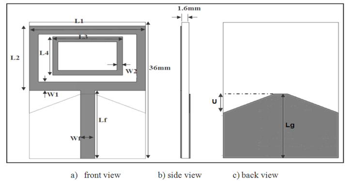
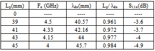
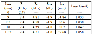
- In this method of band rejection, a certain piece of conducting strip is placed adjacent to the radiating element [12],[16],[26-27]. This added element is called "Parasitic" since it is not directly fed as for the radiating element. The element is designed to resonate at the desired notch frequency. Due to its proximity to the radiating element, the energy is maximum at the resonance frequency. Hence, the current distribution across the radiating element is disturbed leading to reduced gain or increased reflection at the resonance frequency. The notch behavior is exhibited as increased reflection coefficient at the notch frequency. Applying this idea to the dual band dual ring antenna, presented in[24], a modified design is proposed here. The geometry of the dual rectangular ring antenna with the two proposed L-shaped parasitic elements is shown in Fig.(2). The dual rectangular ring radiation patch and the microstrip feed line are etched on the same surface of the substrate, while the tapered rectangular ground and the two L-shaped parasitic elements lie on the opposite surface of the substrate. The parameters of this design are provided in Table (1), and Fig.2-c. The investigations started with studying the effect of varying the length Lp of the two parasitic L-shaped arms, whereas the separation d was set equal to zero (d=0). The reflection coefficient response for various values of the length Lp, when d=0, are shown in Fig. (3). It can be seen that without the parasitic elements (Lp=0), there is no notch in the response at the frequency range of 4-5 GHz. At the notch frequency, the L-shaped line can be considered as a transmission line open-circuited at both of its ends. When the length Lp is increased, the center frequency of notch decreases. The obtained results along with length of parasitic element Lp and S11 achieved are shown in Table (2). It can be seen that at the notch frequency Fn, the length of the parasitic element is almost equal to the effective wavelength, as obtained using Eq. (1). This indicates that, at the notch frequency this element is resonating and leading to a mismatch of the antenna. The reflection coefficients ( for various lengths) at Fn were higher than -4.9dB indicating that at least 25% of the incident power is reflected back. In other words, the reflection coefficient has increased by about 13.5dB in comparison with the case without notching. To obtain better insight into the band-notch operation of the parasitic element, the surface current distribution across the antenna rings and the parasitic element was found using the CST software at Fn =4.5GHz (when Lp=39), is shown in Fig.(4). It can be seen that the current distribution along the parasitic element at the notch frequency is richer than those at other elements, proving that it is at resonance.
 | Figure 1. Geometry of the dual rectangular ring antenna[24] |
 | Figure 2. Geometry of dual rectangular ring antenna with parasitic element |
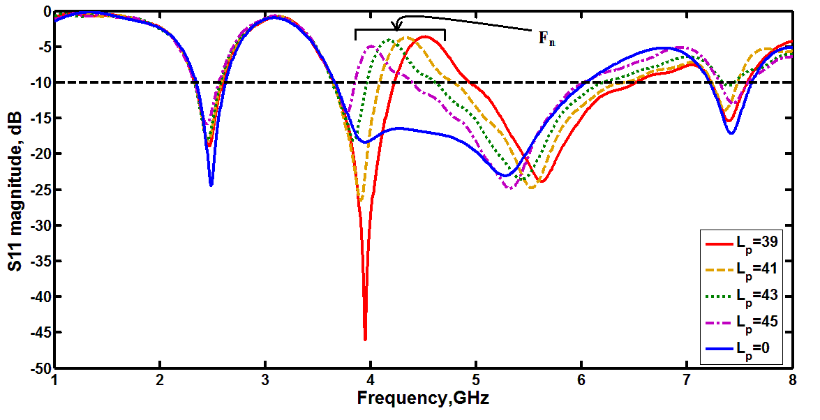 | Figure 3. Reflection coefficient of the dual rectangular antenna with parasitic element showing effect of varying the value of Lp whereas the distance d=0 |
|
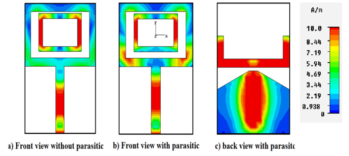 | Figure 4. Surface current distributions of the dual rectangular ring antenna with parasitic element as obtained from the CST software, at the notch frequency (Fn=4.5GHz) |
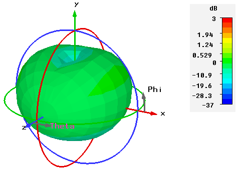 | Figure 5. The three dimensional far-field radiation pattern at notch frequency of Fn=4.5GHz |
|
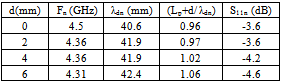
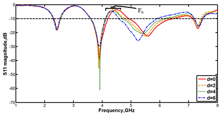 | Figure 6. Reflection coefficient of the dual rectangular antenna with parasitic element showing effects of varying the distance d whereas Lp/2 =19.5mm |
4. U-Shaped Slot
 | Figure 7. Geometry of rectangular antenna with the use of U-slot |
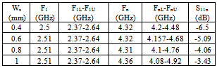
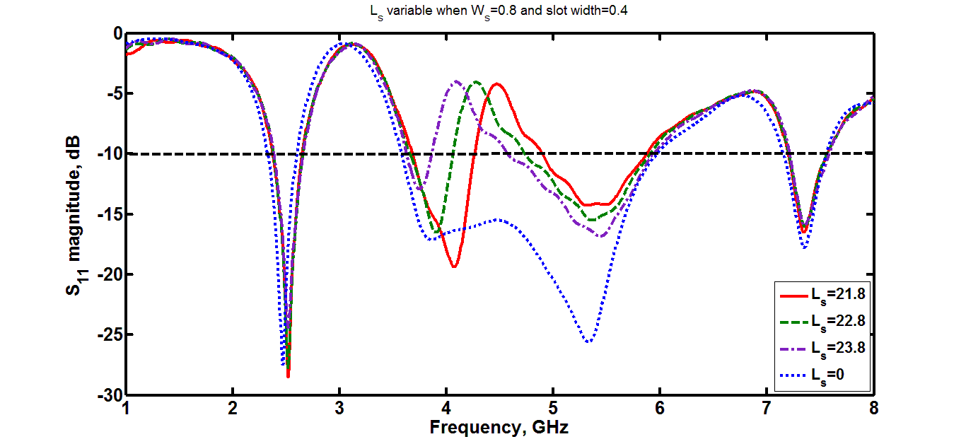 | Figure 8. Reflection coefficient of the rectangular antenna with the U-slot showing effects of varying slot length Ls whereas Ws=0.8 and slot width= 0.4mm |
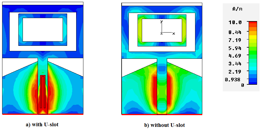 | Figure 9. Surface current distributions of the rectangular antenna with U-slot in the feed line |
|
 | Figure 10. The three dimensional far-field radiation pattern at Fn=4.7GHz |
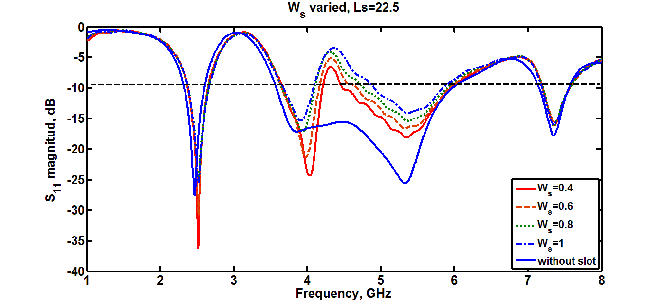 | Figure 11. Reflection coefficient of the rectangular antenna with the U-slot showing the effects of varying slot width Ws whereas Ls=22.5mm |
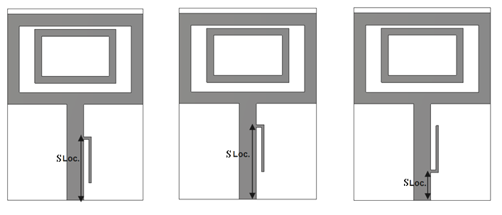
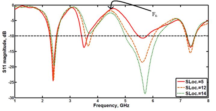
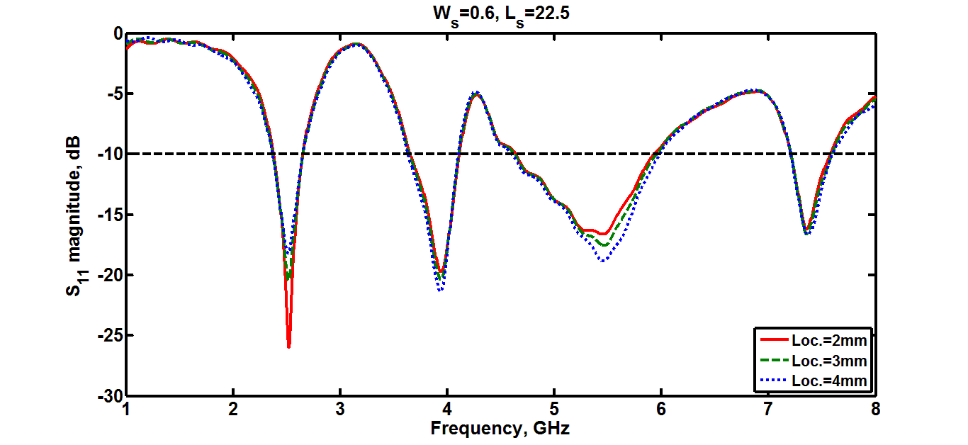 | Figure 12. Reflection coefficient for several locations of the U-slot along the feed line. Ls=22.5, Ws=0.6 |
|
5. The λ/4 Stub
- A stub with an open end etched on the side of the feed line with a length approximately equal to quarter of the effective wavelength is the third method used for band rejection [17,18]. At resonance the open-circuit stub forms a short circuit at the feed line, thus reducing the power supplied to the antenna. The input impedance of an open circuited transmission line of length L is given by[29].
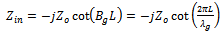 | (2) |
|
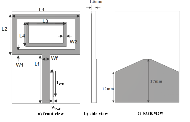 | Figure 13. Geometry of dual rectangular ring antenna with λ/4 stub for band-reject purpose |
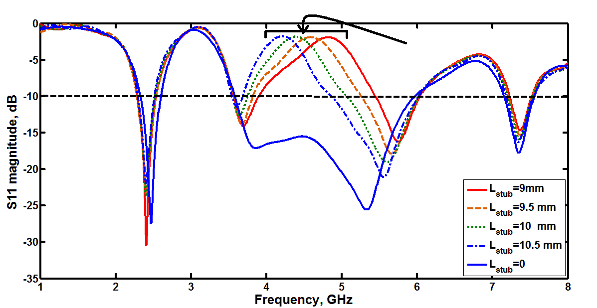 | Figure 14. Reflection coefficient characteristics for four different stub lengths |
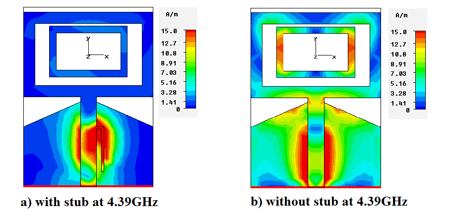 | Figure 15. Surface current distributions of the investigated rectangular dual ring antenna; (a) with λ/4 stub, (b) without stub |
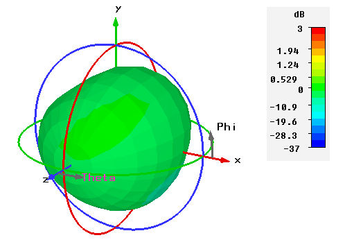 | Figure 16. The three dimensional far-field radiation pattern at Fn=4.39GHz with the λ/4 stub in the right side of the feed line as obtained from the CST |
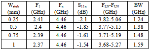
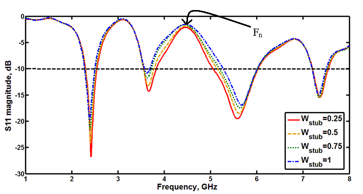 | Figure 17. Reflection coefficient characteristic for different widths of the λ/4 stub. Ls=10mm, Fn =4.46 |
|
5.1. The Effect of Stub Shape and its Position along the Feed Line
- To demonstrate the effect of stub position, three different locations of the stub along the feed line were considered. The obtained reflection coefficient results are shown in Fig.(19). When the stub is placed near the feed point the second band almost vanished, while moving the stub away from the feed point the response improved, illustrating that the stub and feed line operate as transmission line matching elements as expected.The geometry of the λ/4 stub was also studied and the obtained results for the three shapes, shown in Fig.(20), are depicted in Fig.(21). Figure (21) demonstrates that the L-shape yields the best results. The little effect on the first band and the narrower band-notch made the L-shape as the better choice.
 | Figure 18. Geometry of dual rectangular ring antenna with λ/4 stub etched at three different locations along the feed line |
 | Figure 19. Reflection coefficient characteristic for several locations of the λ/4 stub along the feed line |
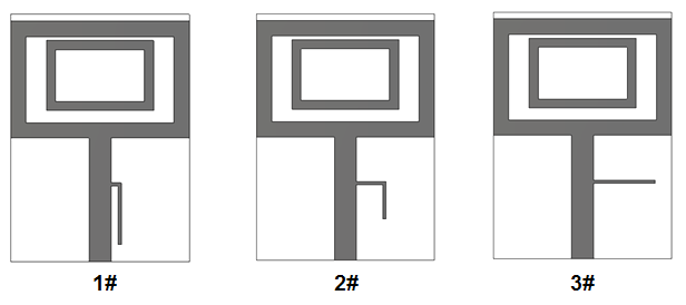 | Figure 20. Geometry of dual rectangular ring with 3 shapes of the λ/4 stub |
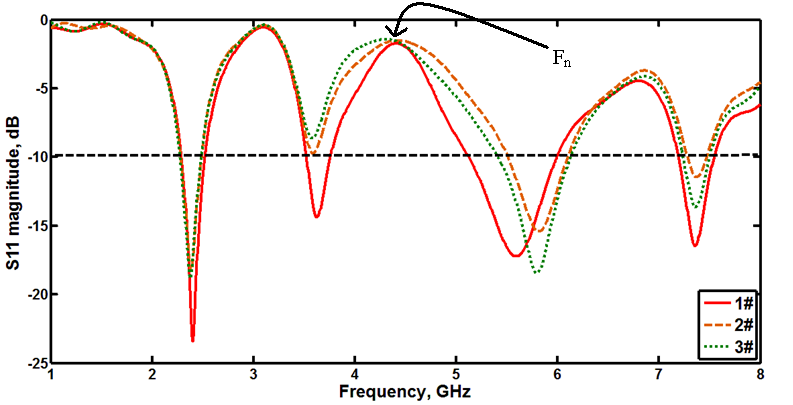 | Figure 21. Reflection coefficient characteristics for the 3 shapes of the λ/4 stub |
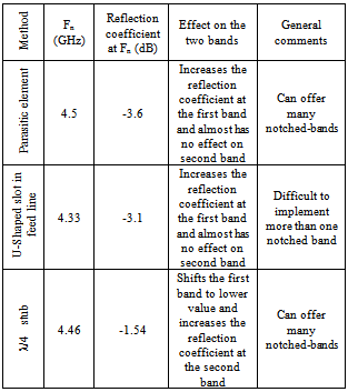
6. Comparison Between the Three Band Notch Techniques
- A comparison between the performance of the three band reject techniques investigated in this paper is shown in Table (8). The use of the λ/4 stub provides the highest reflection coefficient as compared to the other two methods. The U-shape slot and the λ/4 stub have the ability to control the notch band by varying the width of the slot or the stub. The U-shape slot has no effect on the size of the antenna but the stub and the parasitic element suffer from increased complexity and possibly increased size of the antenna if they are not placed properly.
|
7. Conclusions
- Three known band-notching techniques have been investigated by computer simulations. They include the use of; parasitic elements, slots, and stubs. For the three approaches considered, the added element is designed to resonate at the notch frequency. At the notch band, the added element disturbs the current distribution in the radiating patch leading to reduced radiation. In an alternative approach the added element produces high reflection coefficient at the notch frequency. It was shown that, the use of the λ/4 stub provides the highest reflection coefficient as compared to the other methods. The U-shape slot and the λ/4 stub have the ability to control the width of notch band by varying the width of the slot or the stub. The U-shape slot has no effect on the size of the antenna but the stub and the parasitic element increases the complexity and possibly will increase the size of the antenna if they are not properly placed.