-
Paper Information
- Next Paper
- Previous Paper
- Paper Submission
-
Journal Information
- About This Journal
- Editorial Board
- Current Issue
- Archive
- Author Guidelines
- Contact Us
International Journal of Electromagnetics and Applications
p-ISSN: 2168-5037 e-ISSN: 2168-5045
2012; 2(6): 174-181
doi: 10.5923/j.ijea.20120206.07
Loss Computation of Multilayer Coplanar Waveguide using Single Layer Reduction Method
 Abstract
 Reference
 Full-Text PDF
 Full-Text HTML
A. K. Verma , Paramjeet Singh
Department of Electronic Science University of Delhi South Campus, New Delhi 110021, India
Correspondence to: Paramjeet Singh , Department of Electronic Science University of Delhi South Campus, New Delhi 110021, India.
| Email: |  |
Copyright © 2012 Scientific & Academic Publishing. All Rights Reserved.
In this paper, the quasi-static spectral domain approach (SDA) and single layer reduction (SLR) method applicable for multilayer coplanar waveguide (CPW) on isotropic dielectric substrate that incorporates two layer model of conductor thickness is used to compute the impedance, effective dielectric constant, dielectric loss and conductor loss. The transverse transmission line (TTL) technique is used to find the Green’s function for the multilayer CPW in Fourier domain. Dielectric loss of multilayer coplanar waveguide is computed by converting multilayer CPW structure into equivalent single layer CPW using SLR method. Perturbation method is used to compute the conductor loss. The effect of finite conductor thickness is analysed on the impedance, effective dielectric constant, dielectric loss and conductor loss. The present formulation also accounts for low frequency dispersion in computation of quasi-static effective dielectric constant and characteristic impedance.
Keywords: Conductor Loss, Dielectric Loss, Multilayer Coplanar Waveguide, Quasi-Static Spectral Domain Approach, Single Layer Reduction Method, Transverse Transmission Line Technique
Cite this paper: A. K. Verma , Paramjeet Singh , "Loss Computation of Multilayer Coplanar Waveguide using Single Layer Reduction Method", International Journal of Electromagnetics and Applications, Vol. 2 No. 6, 2012, pp. 174-181. doi: 10.5923/j.ijea.20120206.07.
Article Outline
1. Introduction
- There has been a growing interest in different configurations of coplanar waveguide (CPW) transmission line such as conductor backed CPW, CPW with finite ground width, shielded multilayer CPW, elevated or suspended CPW, asymmetric CPW etc. The CPW offers many advantages over microstrip line such as easy connection of both series and shunt components without drilling holes through the dielectric substrate, less dispersive and provides ease of controlling the characteristics of line by changing the strip and slot width. Therefore, CPW transmission lines are widely used in the design of components and interconnect in modern microwave circuit design. The accurate modelling of transmission lines is important in the design and development of modern integrated circuits. Most research done in literature on CPW was based under the assumption of zero conductor thickness using the conformal mapping and spectral domain approach (SDA) method. But in practical cases, the conductor thickness can not be zero and affects the impedance, effective dielectric constant and losses etc. Several research papers have been presented to characterize planar transmission line structure with finite metallization thickness[1-13].This paper presents the effects of finite strip thickness on the impedance, effective relative permittivity, dielectric loss and conductor loss of multilayer CPW structures using quasi-static SDA method on isotropic dielectric substrate. Dispersion characteristics of multilayer CPW is also analysed using single layer reduction (SLR) method.
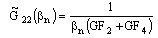
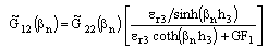
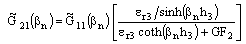
2. Coplanar Waveguide Analysis
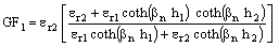
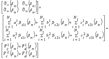
- The conventional CPW consist of centred conductor between two infinite ground planes with all on the same plane. The height of substrate is also infinite. But in practical case, both the width of the ground planes and height of substrate are finite. The cross section structure of shielded multilayer coplanar waveguide of finite conductor thickness under investigation using the quasi-static SDA formulation is shown in Figure. 1. In this paper an efficient method for calculating the line capacitance of shielded multilayer CPW of finite conductor thickness is presented. The effect of conductor thickness is accounted by accommodating the two layer strip conductor model that is suggested for a microstrip line[4]. The potential and charge distribution basis function on the strips is required to compute the line capacitance. The potential on the strips is expressed in terms of charge distribution on the upper and lower strips. The unknown charge distribution function can be expanded in term of linear combination of basis function. The total potential in the range[0, L] is equal to the sum of the potential on strips conductor and potential in two slot region. Then, Galerkin method is applied to find the unknown coefficient of chare density basis function. The total charge on the coplanar waveguide is sum of charge at upper and lower strip of centre conductor. Therefore, quasi-static SDA obtains the total charge on the central strip. By using the total charge on the central strip the per unit length capacitance is computed. The effective dielectric constant and characteristic impedance of the CPW transmission line can be determined using capacitance per unit length.
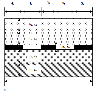 | Figure 1. Multilayer Shielded Coplanar Waveguide |
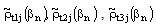
 the number of basis terms of the corresponding strips. The Fourier transform of these basis functions of charge density on central conductor of width , left ground G1 and right ground G2 are
  respectively. In the spectral domain, the charge density basis function for lower and upper surface of conductor plane is given by-
 | (1) |
 and
and  are unknown constant coefficients associated with central conductor, left ground and right ground respectively for lower and upper surface of the conductor,
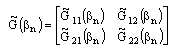
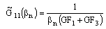
  is number of basis function. The Green’s function and the basis function in Fourier domain are related to potential on strip and slot region by following expression,
 | (2) |
 is potential on dielectric slot region and
  is the potential on conductor strip region. The potential at lower and upper surface of the conductor are
  and
and 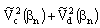 respectively.
 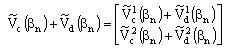 | (3) |
 | (4) |
 | (5a) |
 | (5b) |
 | (5c) |
 | (5d) |
 | (5e) |
 | (5f) |
 | (5g) |
 | (5h) |
 | (6) |
 and applying the Parseval’s identity. By Galerkin’s method solve for the unknown constant of the charge basis function The line capacitance per unit length of finite conductor thickness CPW is computed by substituting the constants in Eq. (7).
 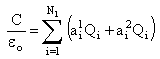 | (7) |
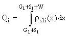 The following charge distribution basis function on central and ground conductor strip is used[14].
 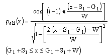 | (8a) |
 | (8b) |
 | (8c) |
 of CPW are computed from the line capacitance of the structure filled with dielectric
  and air
  from the following equations,
 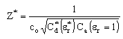 | (9) |
 | (10) |
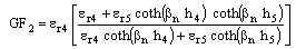
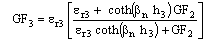
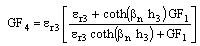
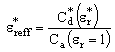
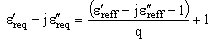
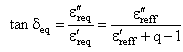
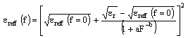
 is the velocity of light in free space.Dielectric loss of multilayer CPW is calculated by converting multilayer CPW structure into equivalent single layer CPW structure using SLR method. The complex effective relative permittivity is computed by -
 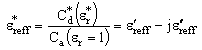 | (11) |
 | (12) |
 | (13) |
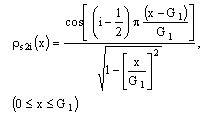
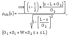
 is filling factor for coplanar waveguide. The dielectric loss[15] of the coplanar waveguide is given by,
 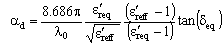 | (14) |
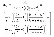 | (15) |
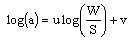
 is complete elliptic integral of first kind,
  is stopping distance,
 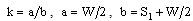 . For symmetric configuration of CPW structure S1=S2=S. where
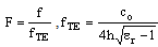
  For single ground coplanar waveguide the conductor loss is computed from[9],
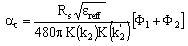 | (16) |
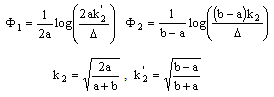
3. Dispersion Analysis of Multilayer CPW
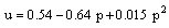
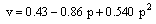
- A dispersion formula[19] for effective dielectric constant has been proposed for coplanar waveguide
 | (17) |
 is the cutoff frequency of the
  mode,
mode, 
 | (18a) |
 | (18b) |
 | (18c) |
 | (18d) |
 . As the frequency decreases, the field penetration inside the conductor increases and effective relative permittivity increases at low frequency.
 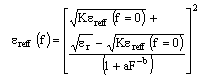 | (19) |
 | (20) |
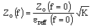
 is the capacitance without skin effect and
  is capacitance with skin effect on air substrate of CPW transmission line.
4. Circuit Model of CPW
- The primary line constants of a multilayer coplanar waveguide are resistance (R), conductance (G), capacitance (C) and inductance (L). These parameters are computed from the conductor loss, dielectric loss, real part of effective relative permittivity and impedance. high dielectric constant disappears at high frequency.
 | (20a) |
 | (20b) |
 | (20c) |
 | (20d) |
 ) and complex propagation constant (
 ) is given by,
 | (21a) |
 | (21b) |
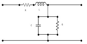 | Figure 2. Circuit Model of Coplanar Waveguide |
 ) Np per unit length, the phase constant is β = Im(
 ) radian per unit length. The effective dielectric constant is calculated from the following relation,
  , where βo is free-space phase constant.
5. Result and Discussion
- In this section, first we have validated the static SDA formulation that include two layer conductor thickness model against EM simulator- Ansoft High Frequency Structure Simulator (HFSS)[20] and Computer Simulation Technology (CST) microwave studio[21].
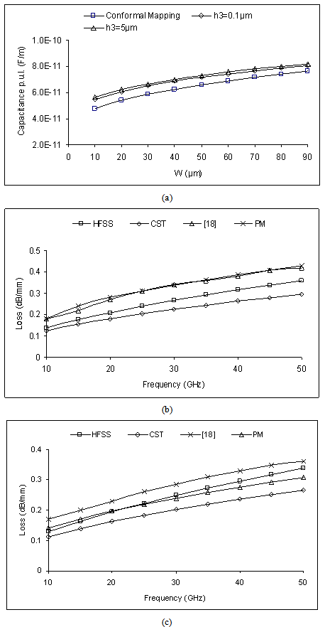 | Figure 3. (a) Variation of Capacitance p.u.l. of CPW with the width of central conductor S1=50μm, S2=50μm, h1=500μm, h2=5μm, h4→∞, εr1=3.78, εr2=12.9, εr4=1.0. Loss versus frequency of coplanar waveguide (b) h3=1.5 µm, (c) h3=3.0 µm, h1→∞, h2=600 µm, h4=0, h5→∞, εr1=1, εr2=12.9, εr5=1, tanδ2=0.0003, W=10 µm, S1=20 µm, σ = 3.0x10⁷ S/m. |
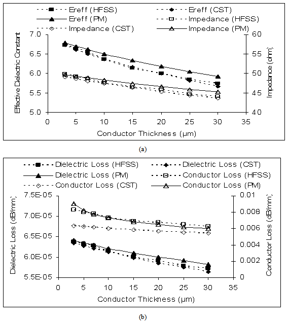 | Figure 4. Variation of (a) Effective dielectric constant and impedance (b) dielectric and conductor loss with conductor thickness of CPW h1=254µm, (b) h2=254 µm, h4=0 µm, h5=10H, εr1=9.8, εr2=12.9, εr5=1, tanδ1=0.0001, tanδ2=0.0003, W=120µm, S1=90µm, σ = 4.1x10⁷ S/m, H= h1+ h2 |
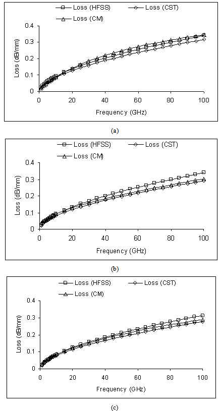
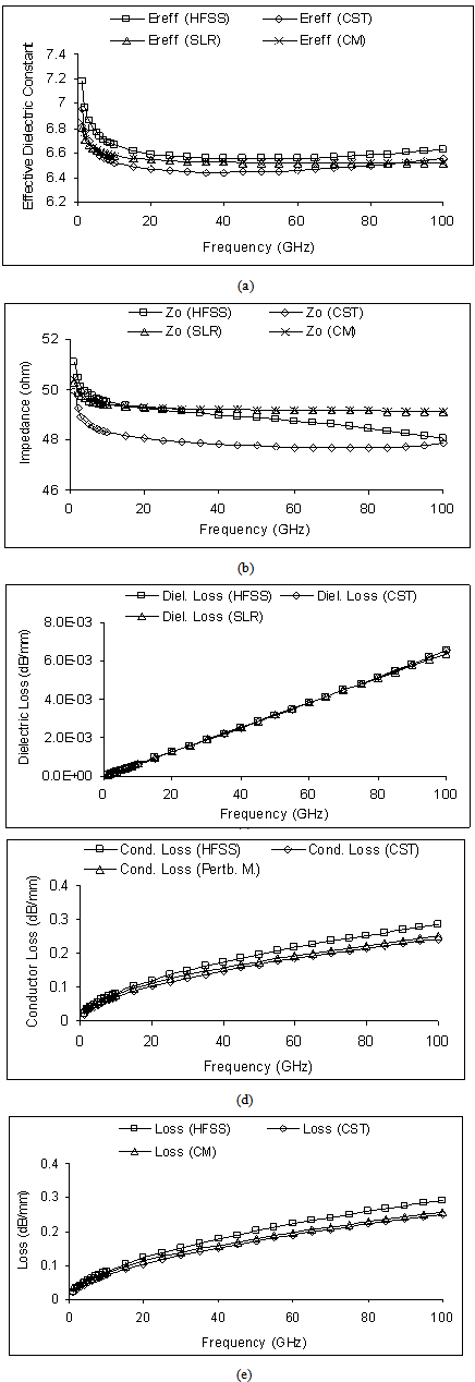 | Figure 5. Propagation characteristics of coplanar waveguide (a) effective dielectric constant (b) impedance (c) dielectric loss (d) conductor loss (e) Total Loss, h1=127 µm, h2=254 µm, h3=3 µm, h4=0, h5=10H, εr1=9.8, εr2=12.9, εr5=1, tanδ1=0.0001, tanδ2=0.0003, W=24 µm, S1=18 µm, σ = 4.1x10⁷ S/m |
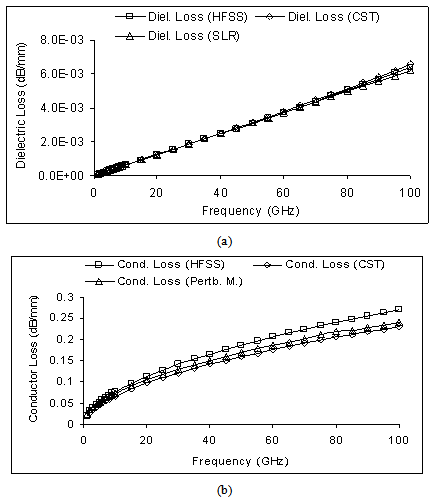 | Figure 6. Losses of coplanar waveguide (a) dielectric loss (b) conductor loss, h1=127 µm, h2=254 µm, h3=5 µm, h4=0, h5=10H, εr1=9.8, εr2=12.9, εr5=1, tanδ1=0.0001, tanδ2=0.0003, W=24 µm, S1=18 µm, σ = 4.1x10⁷ S/m |
 | Figure 7. Attenuation constant of coplanar waveguide with frequency from circuit model (a) h3=1 µm (b) h3=3 µm (c) h3=5 µm, h1=127 µm, h2=254 µm, h4=0, h5=10H, εr1=3.78, εr2=9.6, εr5=1, tanδ1=0.0001, tanδ2=0.0003, W=24 µm, S1=18 µm |
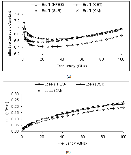 | Figure 8. Multilayer micro coplanar strip (MCS) (a) effective dielectric constant (b) loss, h1=127 µm, h2=254 µm, h3=3 µm, h4=0, h5=10H, εr1=9.8, εr2=12.9, εr5=1, tanδ1=0.0001, tanδ2=0.0003, W=24 µm, S1=18 µm, σ = 4.1x10⁷ S/m |
6. Conclusions
- In this paper, computationally efficient quasi-static SDA is used to study the effect of conductor thickness on effective dielectric constant, impedance, dielectric loss and conductor loss of shielded multilayer CPW on isotropic layered media. The accuracy of the method is investigated through the comparison between results obtained using quasi-static SDA, Ansoft HFSS, CST software and the agreement is very good. The SDA formulation incorporates the two layer model of conductor thickness and concept of permeability due to field penetration in the imperfect conductor. This formulation accounts for the effect of conductor thickness and low frequency dispersion on computation of quasi-static effective relative permittivity and characteristic impedance. The models accuracy is comparable to the accuracy of HFSS and CST, without using complex and time consuming full wave methods. The present formulation can be incorporated in the CAD of CPW based circuits and other planar transmission line with finite conductor thickness conveniently.