-
Paper Information
- Previous Paper
- Paper Submission
-
Journal Information
- About This Journal
- Editorial Board
- Current Issue
- Archive
- Author Guidelines
- Contact Us
International Journal of Electromagnetics and Applications
p-ISSN: 2168-5037 e-ISSN: 2168-5045
2012; 2(5): 129-139
doi: 10.5923/j.ijea.20120205.06
Design of Miniaturized Fractal RFID Tag Antenna with Forced Impedance Matching
 Abstract
 Reference
 Full-Text PDF
 Full-Text HTML
D. K. Naji , J. S. Aziz , R. S. Fyath
Department of Electronic and Communications Engineering., College of Engineering, Al-Nahrain University, Baghdad, Iraq
Correspondence to: R. S. Fyath , Department of Electronic and Communications Engineering., College of Engineering, Al-Nahrain University, Baghdad, Iraq.
| Email: |  |
Copyright © 2012 Scientific & Academic Publishing. All Rights Reserved.
A new optimization based-methodology for miniaturizing RFID tag antenna is introduced. In this paper, the particle swarm optimization (PSO) technique in conjunction with CST Microwave Studio electromagnetic simulator are used to design a miniaturized fractal antenna having perfect impedance matching with the tag chip. The design does not need any additional loading or matching network and hence yields relatively lower cost and smaller antenna size compared with conventional tag antenna systems. A combination of two objective functions related to power reflection coefficient and antenna area are used for optimizing the antenna. The design methodology is applied to a 3rd-order Minkowski fractal nested-slot patch antenna and yields 90% area reduction compared with the reference (non-fractal) counterpart.
Keywords: Minkowski Fractal Antenna, Nested Slot Patch Antenna, PSO, RFID
Article Outline
1. Introduction
- Radio frequency identification (RFID) is the ultimate technology for automatic identification and item-level tracking that experiences an explosive growth in terms of industrial investment and developing applications[1]. As RFID systems grow rapidly, the market demands more features such increasingly cost-effective designs. Further, new emerging applications of RFID systems such as secure identification of bank documents, money bills, and other valuable documents demand low-cost small size tags[2]. For these reasons, there is increasing interest in recent years to design RFID systems operating at the microwave frequencies (for example 5.8 GHz) rather than RF and UHF to ensure small tag antenna size[3-5]. This also opens the possibility to use microstrip patch technology to design efficient RFID antennas[6, 7].Passive tags, which are attached to the identifying objects, contain the antenna and an integrated circuit (where the information related to the object is stored)[8]. A successful communication between the reader and the tag involves a forward link where the reader sends out continuous wave (CW) and commands to the tag. Only as the tag chip receives sufficient power from the CW, it can be turned on and respond to the command[9]. For the maximum power reception, the input impedance of the tag antenna should be conjugate matched to that of the tag chip, or more specifically, the input impedance of the rectifier connected to • Paredes et al.[10] have focused on the design of dual-band impedance-matching networks of interest in RFID systems. By cascading an impedance-matching network between the chip and antenna, the performance of the RFID tags can be improved. The main aim of this study is to demonstrate the possibility of designing such networks by means of split-ring resonators coupled to microstrip transmission lines. These resonators are especially useful in this design since their equivalent circuit substantially simplifies the parameter calculation of the matching network. • Mo and Qin[11] have proposed an open stub feed planar patch antenna for UHF RFID tag mountable on metallic objects. Compared to conventional short stub feed patch antenna used for UHF RFID tag, the open stub feed patch antenna has planar structure which can decrease the manufacturing cost of the tags. Moreover, the open stub feed makes the impedance of the patch antenna be tuned in a large scale for conjugate impedance matching. • Kuo and Liao[12] have presented a method for computing antenna impedance of a patch-type RFID tag. In order to perform impedance calculation in a very short time, an analytic model has been proposed, and the result is highly agreeable with that obtained by the commercial software. Two important parameters are also identified for the purpose of independent impedance tuning of the real and imaginary parts. A prototype has been designed and manufactured based on the proposed method, showing a dimension of 118x43x1.5 mm2 and a reading range of 6 m at f = 915 MHz. • Chen and Tsao[13] have presented the capacitively coupled feeding technique via open-ended microstrip line to perform a complex impedance matching broadband operation. • Qing et. al.[14] have presented an experimental methodology for the characterization of the impedance of balanced RFID tag antennas, and the application of the proposed method in RFID tag co-design has been demonstrated. The co-designed tag antenna achieves conjugate matching with the application-specific integrated circuit so that the reading range of the RFID tag is greatly enhanced. • Kim and Yeo[15] have proposed tag antenna which can be considered as a cavity backed antenna and it is comprised of a bowtie antenna installed in a recessed cubic volume in a large metallic object, and the input impedance of the bowtie antenna can be easily matched by adjusting the coupling effect between the tag antenna and the cavity. Main parameters affecting the coupling are the dimensions of the cavity and the location of the bowtie antenna inside the cavity. For more practical analysis of the impedance matching process, an equivalent-circuit model consisting of several lumped elements has been introduced and each element is optimized using a genetic algorithm (GA). • Braaten[16] has presented a novel compact planar antenna for passive UHF RFID tags. Instead of using meander-line sections, much smaller open complementary split ring resonator particles have been connected in series to create a small dipole with a conjugate match to the power harvesting circuit on the passive RFID tag. (i) Inserting matching network or stub lines between the antenna and the chip[10, 11], (Figure 1(a)).(ii) Loading the antenna in capacitively or inductively manner with small loop or short or open stub line to adjust the antenna input impedance in order to ensure ZA=ZC*[12, 13], (Figure 1(b)).(iii) Reshaping or modifying the antenna geometry, for example, using a typical asymmetrical balanced dipole antenna[14], inserting the antenna in a recessed cavity[15], employing a nested, shaped slot[17], or designing the antenna with series connected open complementary split ring resonator[16], (Figure 1(c)).All these techniques require the insertion of additional elements and/or characterized by a larger area size compared with the conventional counterparts.In this paper a new methodology is proposed to design tag antenna operating with perfect matching with the tag chip. The methodology is based on tuning the geometrical parameters of the antenna to vary its input impedance till it reaches the conjugate of the input impedance of the tag chip at the resonance frequency (see Figure 1(d)). The methodology is enhanced further to design miniaturized antenna under conjugate matching environment by introducing fractal geometry on the reference patch followed by applying PSO technique to address area optimization of the resultant antenna. The degree of impedance matching is estimated using CST Microwave Studio (CST MWS) software which works synchronously with the PSO technique during the optimization process.
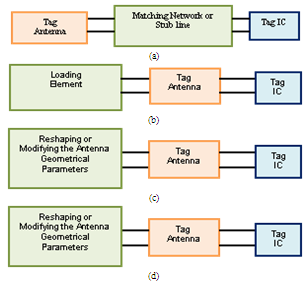 | Figure 1. Matching techniques used for RFID (a) Impedance matching network or stub line (b) Loading elements (c) Reshaping or modifying the antenna geometrical parameters (d) Tuning the antenna geometrical parameters via optimization |
2. System Model and Design Procedure
- The architecture of the passive microwave RFID Tag under investigation is shown in Figure 2. The coupling element between the reader antenna and the chip is a patch antenna. A rectifier converts the input alternating voltage into a dc voltage, which is used by a series voltage regulator to provide the regulated voltage required for the correct operation of the tag. The voltage rectifier is matched with the antenna in order to ensure the maximum power transfer from the tag antenna to the input of the rectifier. A backscatter modulator is used to modulate the impedance seen by the tag antenna, when transmitting. The RF section is then connected to the digital section, which typically is a very simple microprocessor or a finite-state machine able to manage the communication protocol.
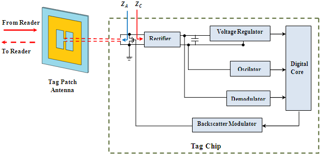 | Figure 2. Passive tag architecture |
 | (1) |
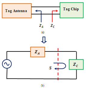 | Figure 3. Simplified block diagram (a) and equivalent circuit (b) of a passive RFID tag |
 | (2) |
 . Since the chip includes an energy storage stage, its input reactance is strongly capacitive. The chip impedance takes the form, ZC = RC + j XC, with XC is negative. Therefore, for perfect matching ZA should be inductive, (i.e., ZA = RA + j XA with XA is positive).Recall that the fitness function requires the calculation of the return loss S11. Unfortunately, the CST MWS can calculate S11 and S for only real load
 . Therefore, an indirect method is adopted here to calculate S for complex values of
 . The method is based on calculating the input impedance of the antenna using CST MWS and then using the results to deduce the value of
 . Hence, the power reflection coefficient
  or PRC is calculated as
 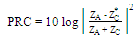 | (3a) |
 | (3b) |
 | (3c) |
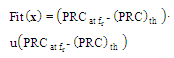
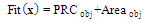
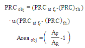
 . The following steps are used for designing the miniaturized antenna under complex matching condition (see Figure 4)(i) Design the non-fractal patch reference antenna (RA) where fractal geometry will be embedded on it in the next step. The antenna geometrical parameters are deduced using PSO in conjunction with CST MWS to ensure 5.8GHZ resonance frequency under the constraint that PRC is equal to or less than a threshold value (
 This constraint ensures high degree of impedance matching.(ii) Insert the fractal geometry on the patch slot of RA and then optimize the generated fractal antenna using a fitness function that takes into account the antenna area and the degree of impedance matching (PRC performance). The design yields a miniaturized antenna (with respect to the RA) with high degree of impedance matching through satisfying
  at the resonance frequency fr = 5.8 GHz.
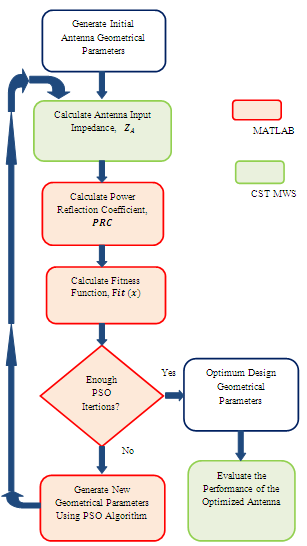 | Figure 4. Data flow for designing both optimized reference and the miniaturized fractal RFID tag antennas. In the designing the fractal antenna, the initial antenna geometrical parameters are taken from the optimized RA |
3. Minkowski Fractal Nested-Slot Patch Antenna
- Tag antennas are usually designed using symmetrical geometry with respect to the chip connection. In this section, a design example is given where a nested-slot patch antenna (NSPA) is adopted as the reference antenna with 3rd-order Minkowski fractal geometry is introduced on it. Figure 5 shows the geometry of the reference NSPA used in the design. The main advantageous of using this antenna structure are its low profile, simple geometry, easy integration with monolithic microwave integrated circuits, low cost, easy fabrication, and approximately stable radiation performances. Also, it’s having impedance tuning capability that made it matched to complex load, and the possibility to host electronics packaging[19, 20]. Figure 6 represents the configuration of the first three orders of the proposed Minkowski fractal nested-slot patch antenna (MFNSPA) together with the reference NSPA. The fractal geometry is introduced on the patch slot. In this work, the 3rd-order fractal antenna is to be miniaturized at 5.8GHZ when it is connected to a chip having an input impedance of
 .
.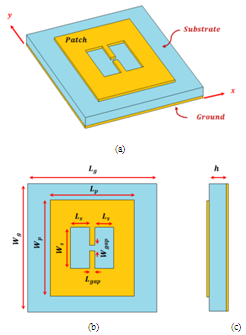 | Figure 5. Reference Minkowski fractal nested-slot patch antenna MFNSPA (a) 3D view (b) front side (c) left side |
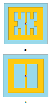 | Figure 6. Minkowski fractal nested-slot patch antenna (MFNSPA) (a) zero-order (reference) (b) 1st-order (c) 2nd-order (d) 3rd-order |
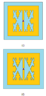 | Figure 6. (Continued) |
3.1. Design of the Reference Antenna
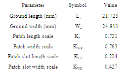
- The initial values of the geometrical parameters of the conventional patch antennas are usually determined using basic analytical (approximated) equations. Then the geometrical parameters are tuned by trial-and-error method to ensure the required resonance frequency. This approach cannot be applied here to design the nested patch RA due to the imposed condition of conjugate impedance matching in addition to the presence of nested slot in the antenna configuration. Therefore, an optimization technique based on PSO algorithm operating in synchronically with CST are adapted to design a RA that satisfies both complex impedance matching condition and the required resonance frequency. The PSO algorithm adopted here is a basic one follows closely with that in Ref.[21]. The patch RA, whose slot radiator is implemented on an FR4 substrate with relative permittivity of 4.3, dielectric loss tangent of 0.025 and substrate thickness of
 is designed to achieve perfect impedance matching at
  through using the following optimization model
 | (4) |
 where
where  is the value of PRC at the resonance frequency and
  is the unit step function. The optimization process is finished whenever the fitness function in (4) is zero, i.e.,
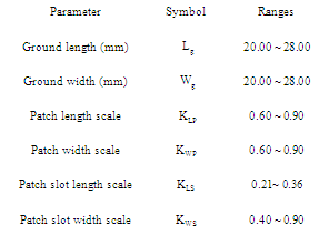
  .As shown in Figure 5, there are six geometrical parameters common to the all fractal orders. These parameters are ground length
 , ground width
 , patch length
 , patch width
 , slot length
  and slot width
 . The parameter
  and
and  are considered as the main parameters where other geometrical parameters are scaled from them. The feeding port parameters, gap length
 , and gap width
  are both set to
 . The following equations describe the relations among the geometrical parameters with the main parameters
 | (5a) |
 | (5b) |
 | (5c) |
 | (5d) |
 are scaling factors. Further, there are additional four geometrical parameters associated with the fractal shape, two are related to slot lengths,
  , and two related to slot width,
  and
and  .To prevent failure in antenna geometrical configuration during the optimization process, the slot length geometrical parameter
  must be ranges within the limit
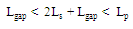 | (6a) |
 | (6b) |
 with input impedance,
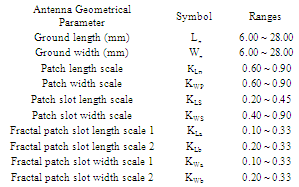
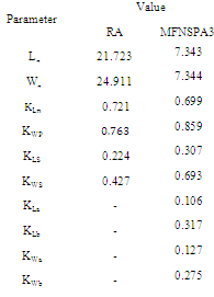
  . The ranges of the geometrical parameters of the RA used in the optimization are illustrated in Table 1. The ranges of ground length
  and ground width
  are chosen here to guarantee that the antenna will resonate at λ 5.8GHz/2 ≈ 25 mm.
|
3.2. PSO Behavior and Optimized Geometrical Parameters of RA
- The number of particles used to optimize RA is 24 particles, 4 for each one of the six geometrical parameters. The criteria used to stop the optimization process is that whenever the power reflection coefficient equals to or less than
 (i.e., the unit step function becomes zero). The optimization procedure here doesn’t search for a minimum area but for any design that yields
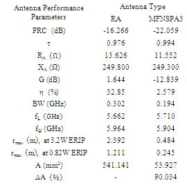
 at the resonance frequency, i.e., any solution satisfy this condition, the optimization process will be stopped. Figure 7 shows the performance progress in the optimization process. Part (a) of this figure displays the best fitness function (solid line) at each iteration (among the 24 particles) and the best fitness function to the current iteration (‘o’ mark). Part (b) shows the variation of power reflection coefficient, PRC with PSO iteration number. It is seen from Figure 7(a) that the fitness function equals to zero at the 36th iteration. At this point, PRC equals to -16.22dB (Figure 7(b)).
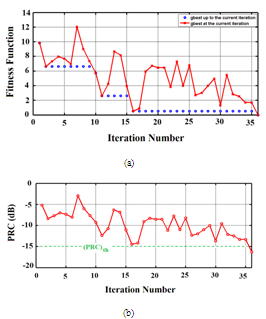 | Figure 7. Variation of fitness function (a) and PRC (b) with PSO iteration number for the RA |
|

 | (7a) |
 | (7b) |
 | (7c) |
 represent, respectively, the area of the RA and the fractal antenna.The geometrical parameters that enter the optimization process are ten, six parameters are common with RA and the other four parameters come from fractal shape introduced in the slot of the patch. Thus the number of particles required to perform the optimization are 30 particles, three for each parameter. A stop criterion is chosen such that 60 PSO iterations are reached or the fitness function remains unchanged with less than 2% error for at least 20 successive iterations. The constraints used in the optimization process for the geometrical parameters of MFNSPA3 are illustrated in Table 3
|
3.3. PSO Behavior and Optimized Geometrical Parameters of MFNSPA3
- The performance progress of optimization process for the MFNSPA3 is displayed in Figure 8. Part (a) of this figure shows total fitness function while PRC and area objectives are plotted in part (b). One can see the rapid speed in optimization convergence (represented by blue circles to indicate the best optimum up to the current iteration). On the other hand, Figure 8(b) depicts that the global optimization (minimum area with PRC less than
 of
of  occurs at 45th iteration.
 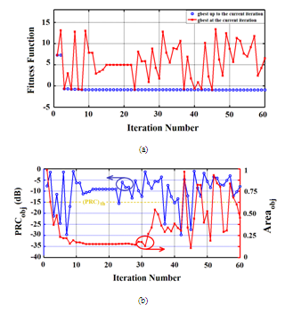 | Figure 8. Variation of fitness functions with PSO iteration number for MFNSPA3; (a) PRC fitness and Area fitness, (b) Total fitness |
 compared to the RA, where
 | (8) |
|
4. Performance Results of the Optimized Antennas
- The electromagnetic properties of the optimized antennas (reference and fractal) are simulated using CST MWS. Results are presented for both optimized fractal and reference antennas.
4.1. Power Reflection Coefficient and Impedance Characteristics
- The frequency dependence of power reflection coefficient, PRC and power transmission coefficient,
 for the two antennas are shown in Figures 9(a) and (b), respectively. It’s seen from Figure 9(a) that MFNSPA3 has one resonance frequency at 5.8GHZ with PRC of
  . In contrast, RA has two resonance frequencies, one at 5.8 GHz with PRC of
  and the other at
  with PRC of
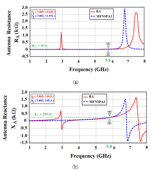
  . Figure 10 presents the spectra of the input resistance and reactance of the two antennas as function of frequency. Its clear that good conjugate matching has achieved and also the self resonance of MFNSPA3 is less than of upper self resonance of RA. Also an interesting behavior is noticed from viewing reactances curves that both antennas have equivalent inductive reactance at low frequencies beyond
 . This is necessary for conjugate matching with capacitive load that represented the chip impedance.
 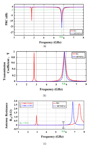 | Figure 9. Results of (a) PRC and (b) power transmission coefficient, τ of the designed antennas |
 | Figure 10. Frequency dependence of the input impedances of the optimized antennas (a) Resistance (b) Reactance |
4.2. Radiation Performance
- In order to simulate the radiation performance of these antennas using CST, a lumped element (a 10Ω-resistor in series with 0.11nF -capacitor) corresponding to the tag chip impedance at 5.8GHz is added in series with the discrete port to ensure complex matching condition. Figure 11 shows the two antennas that simulated under the connection of lumped element (blue) to 50Ω discrete port (red). This is different from the default connection when only a 50Ω discrete port is connected to the antenna to simulate antenna impedance without connection of any load.
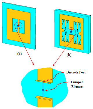 | Figure 11. Antenna configuration after adding a lumped element (blue) representing the load (chip). The lumped element is connected in series with the 50Ω-discrete port (red) to model the tag antenna with chip (a) RA and (b) MFNSPA3 |
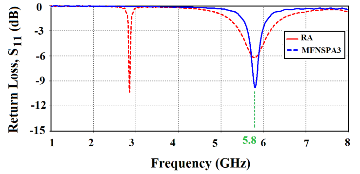 | Figure 12. Return loss S11 of the RA and MFNSPA3 |

 for RA and fractal antenna, respectively. Thus, the complex impedance matching condition adopted in the antenna miniaturization is guaranteed.The variation of peak gain and efficiency of both antennas across the operating bands are drawn in Figure 13. The peak gain corresponds to the frequency where perfect-impedance matching is satisfied. It is worth to note here that introducing the fractal geometry will decrease the gain and the efficiency of the antenna. At 5.8GHz, the gain and efficiency of the fractal antenna are
  and 2.58%, respectively. These values are to be compared with
  and 32.85% for the RA.
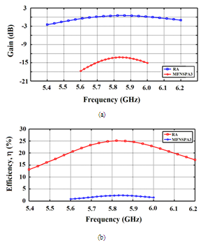 | Figure 13. Gain (a) and efficiency (b) of the optimized antennas |
 can be calculated using Friis free-space formula as[22]
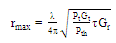 | (9) |
 is the wavelength,
  is the gain of the tag antenna,
  is the power transmitted by the reader,
  is the gain of the transmitted antenna. The times of
  is called ERIP (Equivalent Radiated Isotropic Power) and
  represents the minimum threshold power that required to provide enough power to activate an RFID tag microchip.
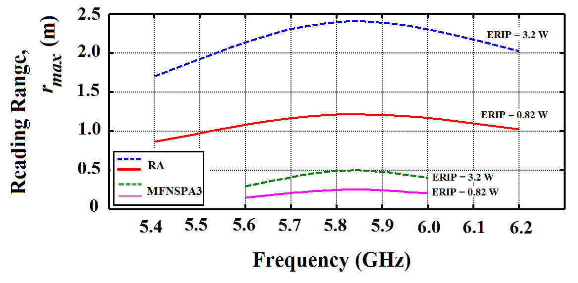 | Figure 14. Reading ranges of the optimized antennas as a function of frequency |
 . It can be observed that both RFID tags are functional across the entire ISM frequency band of
  . At 5.8GHz and ERIP of 3.2W , the reading range decreases from 2.392m to 0.484m when the RA is replaced by the fractal antenna. These values are to be compared with 1.211m and 0.245m, respectively, at ERIP of 0.82W.
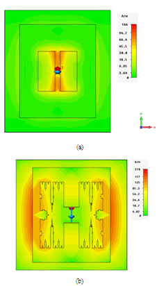 | Figure 15. Simulated surface current distributions on the antenna surface at resonance frequency (a) RA and (b) MFNSPA3 |
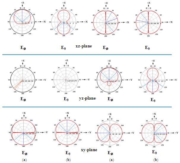 | Figure 16. Radiation patterns for the optimized antennas; (a) RA (b) MFNSPA3 |
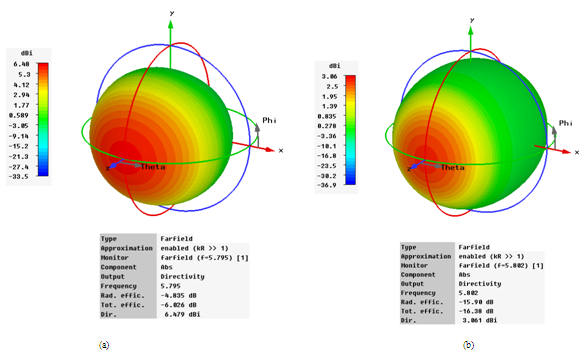 | Figure 17. Directivity of the designed antennas (a) RA (b) MFNSPA3 |
|
 while it is
  for the RA. On the other hand, the two antennas almost satisfy the conjugate matching condition (recall that
 ) and have met the operating frequency of ISM RFID band, which extends,
  .
.5. Conclusions
- The paper has presented the design of a miniaturized 3rd-order Minkowski fractal nested-slot patch antenna for 5.8 GHz RFID passive tag which operates in conjugate impedance matching environment with the tag chip. The design methodology uses PSO technique to minimize the antenna area while keeping high level of conjugate matching with the connected chip. The simulation results reveal that the designed antenna offers 90% area reduction compared with the reference (non-fractal) counterpart. The design methodology can be applied to other antenna structures and configurations and does not need any additional elements to serve as a matching or loading network to ensure conjugate matching condition between the antenna and the tag chip.