-
Paper Information
- Next Paper
- Previous Paper
- Paper Submission
-
Journal Information
- About This Journal
- Editorial Board
- Current Issue
- Archive
- Author Guidelines
- Contact Us
International Journal of Electromagnetics and Applications
p-ISSN: 2168-5037 e-ISSN: 2168-5045
2012; 2(5): 105-113
doi: 10.5923/j.ijea.20120205.03
Effect of Radiated Field Due to ESD on Ones and Zeroes of the Serial Data Stream
 Abstract
 Reference
 Full-Text PDF
 Full-Text HTML
Rajashree Narendra 1, M. L. Sudheer 2
1Dept. of TE, BNMIT, Bangalore, 560070, India
2Dept. of ECE, UVCE, Bangalore, 560001, India
Correspondence to: Rajashree Narendra , Dept. of TE, BNMIT, Bangalore, 560070, India.
| Email: |  |
Copyright © 2012 Scientific & Academic Publishing. All Rights Reserved.
The circuit with an output of specified serial data stream has been exposed to the radiated electromagnetic fields generated by indirect discharge from the ElectroStatic Discharge (ESD) simulator. The circuit malfunctioned at a distance of 35 cm from the point of discharge. The ESD transient pulse introduced affected only the data stream and binary counter Integrated Circuit (IC) SN74LS393N was found to be malfunctioning. The counter IC passed the parameter test but failed functionally as all the output pins were malfunctioning. The circuit that failed did not have decoupling capacitors connected to the Vcc supply. Another circuit designed with decoupling capacitors connected to the Vcc supply of all the IC’s has been exposed to indirect ESD air discharge. The effect of the ESD transient pulse on the ones and zeroes of the specified data stream has been observed. The amplitude of the serial data stream has been affected but the order of transmission of the bits has not changed. If the change in amplitude is greater than the set threshold then the order of transmission of bits can change and this becomes critical for sensitive circuits where the set threshold is very small. The decoupling capacitors provided protection against any malfunction of the integrated circuits.
Keywords: Electrostatic discharge, Transient, Electromagnetic Radiated Fields, ESD Simulator, Indirect discharge, Integrated Circuit, Digital data
Article Outline
1. Introduction
- Malfunctioning of integrated circuits and electronic systems have been mathematically predicted for the circuits exposed to the radiated fields[1, 2] generated by indirect discharge from an ESD simulator[3]. The way in which an IC fails as a result of ESD varies for every case and it is dependent upon a number of factors including the way in which the charge is dissipated to the topology within the IC. One of the most obvious way in which an IC can fail occurs when the static charge represented as a very high voltage gives rise to a high peak current causing burnout. It is quite possible for the voltage to breakdown an insulating oxide layer leaving the IC permanently damaged as in the case of digital devices[4]. Electronic components are often required to survive a maximum of 8kV (contact) or 15kV (air) discharge according to IEC 61000-4-2 ESD standard. Even with suitable ESD protection circuits in the integrated circuits, the IC’s are still damaged by the ESD discharge. In many cases the ESD discharge may be greater, so it is wise to provide additional protection[5-13]. The problem of protection becomes more serious in the circuits which have IC’s not protected with decoupling capacitors at their Vcc terminal. It is necessary to keep the high frequency energy from entering the chip, so the capacitors are used for high frequency decoupling. The decoupling capacitors provide a low impedance path to shunt transient energy to ground at the source[14-16].The ESD indirect discharge test was carried out to verify the ESD immunity of the IC’s used in the circuit generating an output of specified data stream. The malfunctioning of the IC occurred and the ESD transient introduced in the data affected the data stream. This happened only in the circuit which had IC’s without the external protection offered in the form of decoupling capacitors connected at the supply point of the IC. The circuit which had the external protection of decoupling capacitors connected at the supply point had momentary ESD transient introduced in the data stream, but this did not cause malfunctioning of the IC’s or upset the specified data stream. The amplitude of the data is affected which becomes important for the sensitive circuits whose set threshold is very small. So an effective ESD protection solution in the form of decoupling capacitors has been implemented for improving the ESD robustness of the integrated circuits used in the electronic systems.
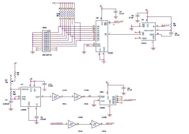
2. Testing of Circuit
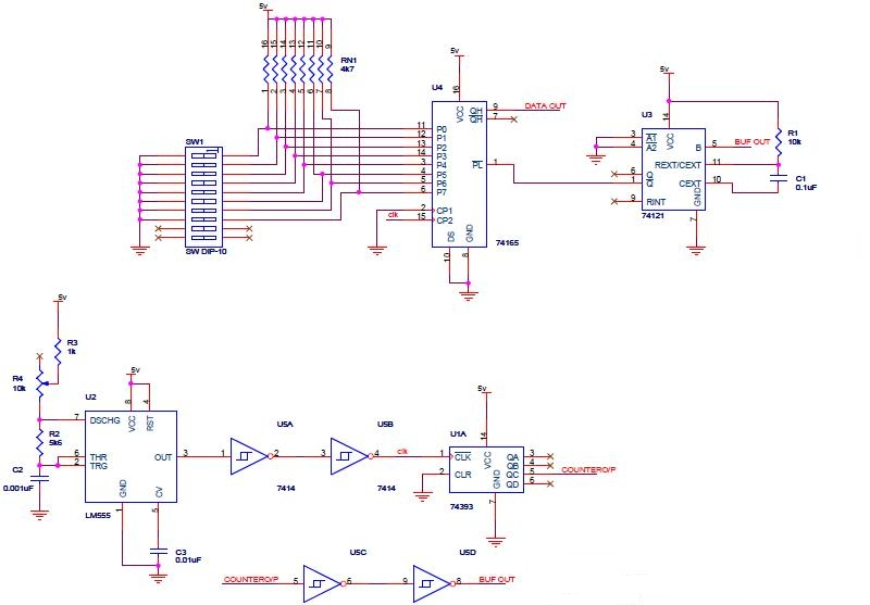
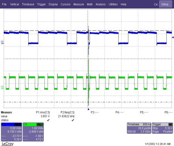
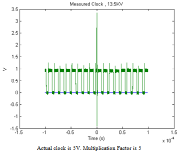
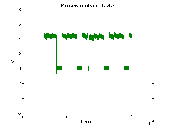
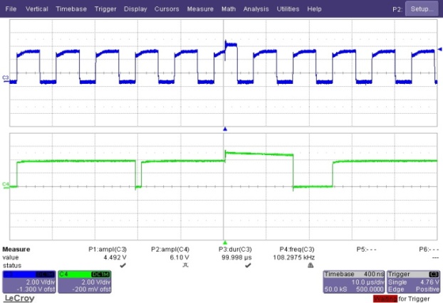
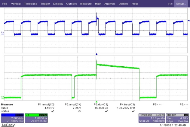
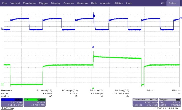
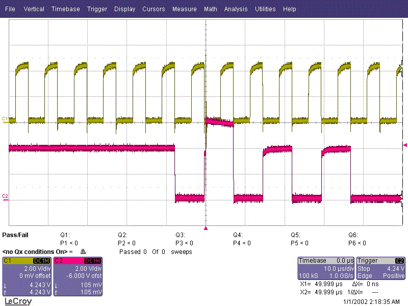
- A simple circuit as shown in Figure 1 is designed which gives an output of specified data stream. The 8 bit data can be changed in the DIP switch provided. We can have a specified stream of one’s and zeroes. The data stream chosen is 01110111. The 555 timer is used for clock generation. The clock frequency can be varied from 62.5 KHz to 118 KHz by varying the 10 KΩ potentiometer. The dual 4 stage binary counter IC 74393 is used as an ÷8 counter. The IC 74121 is a monostable multivibrator which accepts new data after every 16 bits. The IC 74165 is an 8 bit parallel into serial output shift register. The circuit gives an output of specified serial data stream.The experimental setup for the indirect test consisted of an ESD simulator Electrometrics EDS 200 which is used to discharge high voltages onto the horizontal ground plane. The test voltage can be varied from 100V to 25KV. The very short rise time of 0.7 ns to l ns of each single pulse generates a wide RF spectrum and interference. The distance between the ESD discharge point and the circuit under test is varied. The ESD simulator source voltage is set at 13.5 kV. An ESD pulse is air discharged on the horizontal ground plane at a distance of 35cm from the functioning circuit. The clock and serial data stream is monitored on the LeCroy 6100A, 350 MHz Wave runner oscilloscope.A short duration transient is introduced in the data as well as the clock stream as shown in the Figure 2, which affected the data transmission. The clock and data voltage level is set to 5V. The transient introduced in the clock as shown in Figure 3, had a top peak of +16.85V and bottom peak of -7.25V and the data stream as shown in Figure 4, had a top peak of +7.35V and a bottom peak of -4.6V. As soon as the ESD transient is introduced in the clock and data, the data shown at the top in Figure 2 changed from 1 to 0 and also the clock shown at the bottom in Figure 2 momentarily changed from 1 to 0 for 2.5 μs.
3. Analysis of the ESD Test
- An extra 1 has been added in the data stream 011110111. The malfunctioning of the circuit occurred during the ESD event and the data/clock stream continued for the next 16 bits. But when we tried to change the data, the circuit did not output the specified data but the clock pulse stream gave output as specified. Each point in the circuit is checked and the IC’s are also investigated. All the pins of the DIP switch are perfectly working. The Timer IC and Buffer IC are found to be okay. Pin 5 (÷ 8) of the Counter IC SN74LS393N is not giving any output. The IC 74121 monostable multivibrator is not receiving any input at pin 5 (Input B). The data output is thus getting affected at the parallel to serial shift register IC 74165.Since all the other ICs are found to be okay, the SN74LS393N binary counter is sent for failure analysis which included the parameter measurement, functional test and decapping of the packaged IC. The SN74LS393N binary counter passed the parameter measurement test but the device failed functionally (all output pins 3, 4, 5, 6, 8, 9, 10, 11 of counter IC are malfunctioning). The optical microscope has been used to find any ESD damaged failure spots in the silicon die. But the optical micrograph shown in Figure 5 does not reveal any ESD damaged failure spots.
 | Figure 1. Test Circuit exposed to radiated field from an ESD |
 | Figure 2. Effect of ESD Transient on the data and clock |
 | Figure 3. Clock stream with the ESD transient |
 | Figure 4. Data stream with the ESD transient |
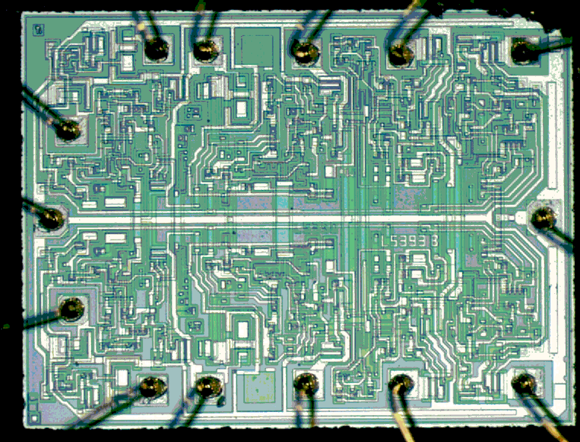 | Figure 5. Optical Topography of IC SN74LS393N (Failed device) |
4. Testing of Circuit with ESD Protection
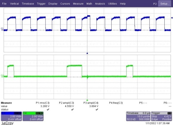
- The malfunctioning of the counter IC and the change in the data stream is analysed. An effective ESD protection solution in the form of decoupling capacitor is considered for improving the ESD robustness of the IC. Another circuit as shown in Figure 6 is designed with the decoupling capacitors of value 0.1μF connected to the Vcc supply of all the IC’s. This circuit is again exposed to radiated field from an ESD generator. An indirect test on the horizontal coupling plane is done for various voltages and distances. A transient spike of lower magnitude is introduced momentarily but it does not affect the clock stream as well as the specified data stream. So the use of decoupling capacitors reduced the impact of the transient on the functioning of the IC’s, which resulted in proper functioning of the circuit. The ESD transient however had an effect on the amplitude of the data stream and its effect on the ones and zeroes of the data stream are observed.
 | Figure 6. Test Circuit with decoupling capacitors |
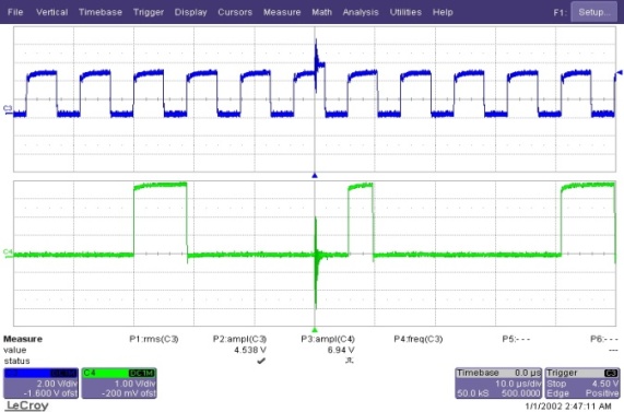
5. Effect of Radiated Field Due to ESD on Ones of the Data Stream
- An ESD pulse is air discharged on the horizontal ground plane at various distances (1 m, 0.5 m and 0.1 m) from the functioning circuit shown in Figure 6. The ESD simulator source voltage is set at 13.5 kV. The pulse is discharged during the transmission of Ones of the serial data stream and is monitored on the LeCroy 6100A, 350 MHz Wave runner oscilloscope. A short duration transient is introduced in the data as well as the clock stream as shown in the Figures 7, 8, and 9, which affects the amplitude of clock and data momentarily but does not affect the order of transmission of clock stream and the data stream[11101111]. In conclusion, it has been observed that when the transient is discharged during the data transmission of ONES, it affects the amplitude of the data but it does not disturb the order of transmission of the bits as the increase in amplitude is well within the threshold limits.Another set of data[01010100] is exposed to the indirect ESD test on horizontal plane at 15kV and at a distance of 0.05 m, the amplitude of the data increased by 2 V as shown in Figure 10. Since the amplitude increase is within the limits of threshold, the order of transmission of the bits did not change.
 | Figure 7. Clock and data stream with ESD transient introduced on ONE data bit at the distance of 1 meter |
 | Figure 8. Clock and data stream with ESD transient introduced on ONE data bit at the distance of 0.5 meter |
 | Figure 9. Clock and data stream with ESD transient introduced on ONE data bit at the distance of 0.1 meter |
 | Figure 10. Clock and data stream with ESD transient introduced on ONE data bit at the distance of 5 cm |
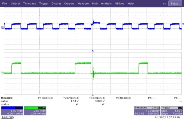
6. Effect of Radiated Field Due to ESD on Zeroes of the Data Stream
 | Figure 11. Clock and data stream with ESD transient introduced on ZERO data bit at the distance of 1 meter |
 | Figure 12. Clock and data stream with ESD transient introduced on ZERO data bit at the distance of 0.5 meter |
 | Figure 13. Clock and data stream with ESD transient introduced on ZERO data bit at the distance of 0.1 meter |
7. Conclusions
- The malfunctioning of the IC’s due to the effect of the radiated fields from an ESD generator and the effect of ESD transient introduced in the serial data stream is investigated. The results on the malfunctioning of the IC and the circuit failure analysis shows that the IC’s need extra external ESD protection. A decoupling capacitor must be connected to the Vcc supply of each of the individual ICs in the given circuit. By using this proposed effective ESD protection scheme, the ESD robustness of the circuit giving specified serial data stream has been improved. The positive peak of the transient introduced in the data stream has decreased from +7.35V to +3.08V. The effect of the ESD transient introduced in the data and clock stream has reduced considerably which resulted in the safe working of the circuit without any malfunction. Also, it has been observed that when the transient is discharged during the data transmission of ONES, it affects the amplitude of the data but it does not disturb the order of transmission of the bits as the increase in amplitude is well within the threshold limits. When the transient is discharged during the data transmission of ZEROES, it does not disturb the amplitude of the data as well as the order of transmission of data bits.
ACKNOWLEDGEMENTS
- Rajashree Narendra would like to thank the EMI/EMC group at LRDE for providing an opportunity to carry out her PhD research work.