Abdu Zubairu1, Abddullahi S. B. Gimba2, Babagan Gutti1, Abddulmalik Audu1
1Department of Chemical Engineering, University of Maiduguri, Borno State, Nigeria
2Department of Petroleum and Gas Engineering, Nile University of Nigeria, Abuja, Nigeria
Correspondence to: Abdu Zubairu, Department of Chemical Engineering, University of Maiduguri, Borno State, Nigeria.
| Email: |  |
Copyright © 2020 The Author(s). Published by Scientific & Academic Publishing.
This work is licensed under the Creative Commons Attribution International License (CC BY).
http://creativecommons.org/licenses/by/4.0/

Abstract
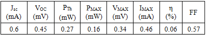
A p-n homo-junction copper (I) oxide (cuprous oxide, Cu2O) solar cell was potentio-statically electro-deposited on an FTO (Fluorine Tin Oxide)-coated glass substrate from a solution containing 0.4M copper (II) sulfate and 3M lactic acid. The deposition was carried out in two stages: in the first stage, n-type cuprous oxide was deposited on the FTO glass substrate using a solution with bath pH of 7.5, and at a constant potential of -0.20V (vs. Ag/AgCl/saturated NaCl) to give a thickness of 16000 Angstrom (1.6µm). While the second stage was characterized with the deposition of a 13000 Angstrom (1.3µm) layer of layer p-type cuprous oxide directly on the already deposited n-cuprous oxide, at a solution pH of 11.56, and applied potential of -0.4V throughout. Bath temperature was maintained at 60°C throughout the deposition processes with continuous stirring. The lactic acid was used to stabilize Cu (II) ions at bath pH higher than 7, while the bath pH was carefully adjusted by the controlled addition of 4M NaOH. The superstrate solar cell configuration has the added advantage of not only serving as a supporting structure, but also as a window for the illumination and as part of the encapsulation. The electrical, structural, and optical characteristics of the cell were well investigated, where values of 0.60mA, 0.453mV, 0.272mW, 0.155mW, 0.336mV, 0.462mA, 0.571 and 0.058% were recorded for the short-circuit current density (JSC), open-circuit voltage (VOC), theoretical power (PTh), maximum power (PMAX), maximum voltage (VMAX), and maximum current (IMAX), fill factor (FF), and efficiency respectively.
Keywords:
Electro-deposition, Cuprous oxide, Homo-junction, Potentiostatic, Solar cell
Cite this paper: Abdu Zubairu, Abddullahi S. B. Gimba, Babagan Gutti, Abddulmalik Audu, Potentiostatic Elehctro-Deposition of p-n Homo-Junction Cuprous Oxide Solar Cells, Energy and Power, Vol. 10 No. 1, 2020, pp. 20-25. doi: 10.5923/j.ep.20201001.03.
1. Introduction
Copper (I) oxide is one of the earliest known semiconductor material and its potential for use in semiconductor devices has been recognized since 1920 [1]. But when it comes to solar cell applications, Cu2O is rarely significant, and this is not unconnected to its low energy conversion efficiency which was said to result from the fact that the light generated charge carriers in micron-sized Cu2O grains were not efficiently transferred to the surface and lost due to recombination [2]. Furthermore, its low efficiency was attributed to the fact that most of the available Cu2O cells then were based on hetero-junctions, and there were reasons to believe that the interface between the p-type Cu2O and other materials constituted a significant loss mechanism for photo-carrier separation and collection. As a solution to this challenge, it was proposed that if the grains radius are reduced from micrometer dimensions to nanometer dimensions, the opportunities for recombination can be dramatically reduced. Thus, the preparation of nano-crystalline Cu2O thin films is becomes a key to improving the performance of solar application devices [2]. Similarly, from many early studies, it has been long held that the formation of a Cu2O p-n homo-junction could also help in improving the efficiencies of these cells [3]. For conventional silicon-based PV solar cells, the manufacturing processes employed is one deeply rooted in the electronic industry, as a result, these solar cells contain most of the chemicals found in e-waste, just as it involves several toxic, flammable and explosive chemicals, most of which pose a great health hazard to the environment [4]. These, coupled with the high cost of silicon solar cells are the primary reasons behind the renewed drive for new photovoltaic devices utilizing cheap and non-toxic materials prepared by energy-efficient processes. Electro-deposition, as one technique from a variety of other low-temperature deposition techniques such as thermal oxidation, anodic oxidation, chemical oxidation, as well as reactive sputtering, exist for the preparation of thin Cu2O films on either Copper or other conducting glass substrates. But, the electro-deposition method remains particularly attractive because of its economy and simplicity [5]. The deposition can either be on metal substrates or on transparent conducting glass slides coated with highly conducting semiconductors, such as indium tin oxide (ITO), fluorine tin oxide (FTO), SnO2, In2O3 etc. [6]; [7].These low-temperature techniques are favoured because the electrical and optical properties of Cu2O thin films deposited at low temperatures are reported to be different and better as compared to those of the thermally oxidised films prepared at high temperatures (approx. 1100°C), such as thermal oxidation [8]. This is due to the expected reduced defect deformation in the low-temperature deposited films, which could arise from thermally induced stresses when high-temperature techniques are employed to deposit the films and it offers precise control of the driving force for the reactions involved in deposition, controlled growth allowing control of the structure, orientation and phase composition of the films so as to fit specific applications [7]; [9]; [10].Therefore, this work aims at reviewing this technique with the intention of adopting it and exploring possibilities of kick starting a pilot plant where such cells will be produced locally, taking advantage of the cheapness and simplicity of the technique as compared to the complex and expensive processes involved in silicon-based solar cells production.This work will include the electro-deposition, characterization, and current-voltage measurements of a cuprous oxide p-n homo-junction solar cell.
2. Theory
2.1. Background
The reason behind the sustained interest on such an old semiconductor even in the presence of many leading and seemingly better alternatives such as Perovskites and organic solar cells was simply attributed to sustainability [2]. This is one of the requirements for a semiconductor to be usable for large scale PV power generation. In addition, it is cheap in terms of cost, it has low toxicity, very attractive electrical and optical properties as well as a good direct band gap energy of 1.7 – 2.2eV, which gives it a relatively high absorption coefficient (approx. 105/cm), comparable to some organic semiconductors [2]; [11]; [12].
2.2. Techniques of Electro-deposition
In electro-deposition, Cu2O is formed on the cathode by reduction of Cu2+ ions from the organic electrolyte. The possible reactions during the cathodic reduction of copper (II) lactate solution are illustrated in equations (1) – (3).  | (1) |
 | (2) |
 | (3) |
The electrodeposition techniques are particularly well suited for the deposition of single elements but it is also possible to carry out simultaneous depositions of several elements and syntheses of well-defined alternating layers of metals and oxides with thicknesses down to a few  [2]. Literatures abound on the use of electrodeposited cuprous oxide as a solar cell material. Some of these include the work of [13] conducted a potentiostatic electro-deposition of cuprous oxide thin film in an acetate bath where they discovered the band gap energy of the semiconductor to be 2.0eV through optical transmission studies.Other workers [14] confirmed the hypothesis that pH of solution can be used to control the native point defects. They did this by electrochemically depositing both p-type and n-type cuprous oxide with different pH of solution. Similarly, [15] adopted a two-step process to deposit a p-n homojunction Cu2O solar cells, with optimized deposition conditions for minimum resistivity. Han [16] fabricated Cu2O p-n homojunction solar cells with two different structures by a two-step electro-deposition method giving a maximum efficiency of only 0.15%. According to Han, the low efficiency of Cu2O solar cells was mainly due to the high resistivity of both the p- and n-Cu2O.Septina et al. [17], undertook the potentiostatic deposition of Cu2O thin films on glass substrates coated with Flourine-doped SnO2 from an alkaline electrolyte solution (pH 12.5) containing copper (II) sulfate and lactic acid obtaining an efficiency of 0.603% and attributing it to the better compactness and purity of the Cu2O film. McShane and Choi [18] conducted Junction Studies on electrochemically fabricated p-n Cu2O homojunction solar cells for efficiency enhancement where they stressed the importance of the use of proper contact materials in solar cell fabrication. At the end of all successful electro-deposition exercises, series of tests were conducted on the deposited cells in order to establish the different parameters of the cells, as well as the structural, optical and electrical properties of the cells. Some of these tests include: X-Ray Diffraction analysis, SEM analysis, Profiler, UV-vis transmittance, and solar simulation (current-voltage characterization). Some important mathematical relationships are presented.From a UV-Vis transmittance spectrum, the band-gap of a semiconductor can be calculated from equation (4).
 | (4) |
Where  represents the photon energy,
  is the band-gap and
  is a constant.
  depends on the nature of the band-gap
  for indirect forbidden transition,
  for indirect allowed transition,
  for direct forbidden transition, and
  for direct allowed transition). The intercept of a
  plot with the
  axis determines the band-gap of the semiconductor.The values of the absorption coefficient,
  , were calculated from equation (5).
 | (5) |
Where  is the film's thickness, in µm, determined using profiler method, and
  is the absorbance determined from the values of transmittance, T(%), using equation (6).
 | (6) |
The fill factor (FF) is most commonly determined from measurements of the IV curve, and is defined as the maximum power divided by the product of  (Open-circuit voltage, mV) and
  (short-circuit current, mA) given by equation (7).
 | (7) |
 is the maximum power (W),
  is the theoretical power (W),
  is the voltage at maximum power (mV), and
  is the current at maximum power (mA). The efficiency of a solar cell is determined as the fraction of incident power which is converted to electricity and is defined as illustrated in equation (8).
 | (8) |
Where  is the input power (W). The input power for efficiency calculations is 1kW/m2 or 100mW/cm2. Thus, the input power for a 100 x 100mm2 cell is 10W and for a 156 x 156 mm2 is 24.3W.
3. Materials and Method
3.1. Electro-deposition
An FTO on a glass substrate was used as a working electrode in the electro-deposition for the fabrication of the Cu2O solar cell with superstrate structure. The counter electrode was a Cu sheet, and the reference electrode was Ag/AgCl/sat. NaCl in an improvised traditional three-electrode chemical cell. The deposition of n- and p-type Cu2O was potentiostatically (at constant potential difference) carried out with stirring. Figure 1 illustrates the experimental set-up.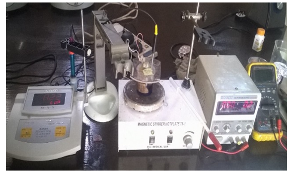 | Figure 1. Experimental Setup for Cu2O electro-deposition |
To make a p-n homo-junction, n- and p-type Cu2O films were sequentially deposited in two electrolyte solutions of the same composition but different pH. n-type Cu2O were first electrochemically deposited on a FTO/glass substrate in an aqueous solution containing 0.4M copper sulphate and 3M lactic acid at the solution pH of 7.5, the deposition potential -0.2 V, and the deposition temperature of 60°C for 60 minutes. Then p-Cu2O were directly deposited on n-Cu2O in an aqueous solution of the same composition (0.4M copper sulphate and 3M lactic acid) at the solution pH 11.56, the deposition potential -0.4 V, and the deposition temperature of 60°C for 10 minutes. All the chemicals used were reagent grade. In adopting the superstrate structure, the actual solar cell materials are deposited above the glass, thus, in the finished device, there is no need for a second glass plate for the encapsulation, as compared to substrate solar cell structures where such is needed. This is because, in the superstrate structure, the glass substrate is not only used as the supporting structure, but also as a window for the illumination and as part of the encapsulation. In addition to this, solar cells with superstrate structures were shown to have lower production costs.
4. Results and Discussion
4.1. XRD Analysis
The structure of the films were studied using X-ray diffraction with CuK α radiation with a wavelength of 1.54 nm. The Bragg angle of 2θ was varied between 4° and 75°. The XRD spectrum of the film sample deposited on glass coated by FTO is shown in Figure 2. It was found out that all films are polycrystalline and chemically pure Cu2O with no traces of CuO, as typical of all most of such depositions. XRD peaks corresponded to Cu2O and the substrate material. The XRD spectrums indicate a strong Cu2O peak with (111) preferential orientation, similar to what was observed in the works of [16], and [19].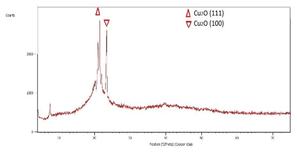 | Figure 2. X-ray diffraction Spectrum for Cu2O deposited on FTO-coated glass substrate |
4.2. SEM Analysis
The surface morphology of the films were studied by a scanning electron microscope EVO, model MA/10 at different magnification levels of x1000, x2000, and x4000 as shown in figures 4 (a), (b), and (c) respectively. All the figures show the scanning electron micrographs of Cu2O films deposited on glass coated by FTO (Fluorine Tin Oxide). The micrographs (at different magnifications) indicate a polycrystalline structure, as can be clearly observed from Figure 3 (a-c). They are about 1µm for the film deposited on FTO. 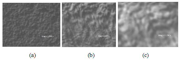 | Figure 3. Micrograph obtained from a scanning electron microscope of Cu2O deposited on FTO ( a: x1000 Mag; b: x21000 Mag; c; x4000 Mag) |
4.3. Profiler
The thickness of the deposited cells were determined each for the n-Cu2O and p-Cu2O using a profiler machine and the results are presented in Figures 4 and 5 respectively.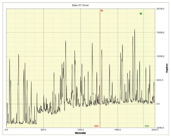 | Figure 4. Graph of the Profiler reading of deposited n-Cu2O film |
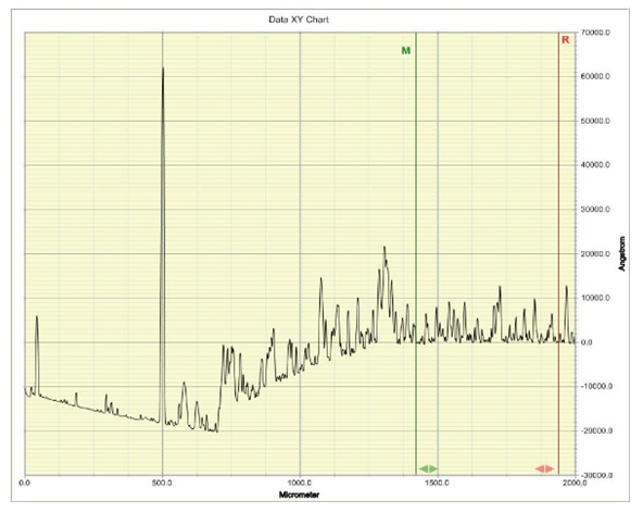 | Figure 5. Graph of the Profiler reading of deposited p-Cu2O film |
The thickness of the films is taken as the highest peak between the R and M lines, and from Figures 4 and 5, the n-type is shown to have a thickness of about 16000 Angstrom, which is equivalent to 1.6µm, while the deposited p-type has a thickness value of about 13000 Angstrom, an equivalent of 1.3µm, respectively. These thicknesses resulted from the different deposition times. While the n-Cu2O was deposited for 60 minutes, the p-Cu2O was deposited for just 10 minutes as recommended in the literature [19]. This is because the applied potential for n-Cu2O deposition is usually kept low, below -0.3 V to avoid deposition of metallic copper. Therefore, the corresponding current is much lower than that of p-type cuprous oxide deposition, which results in a much lower deposition rate of n-type cuprous oxide. Therefore the deposition time for n-type cuprous oxide is much longer.
4.4. Optical Band-Gap Energy Determination (UV Spectrophotometry)
The optical band-gap is an essential parameter for semiconductor material, especially in photovoltaic conversion. In this work it was determined using the transmittance spectrums of the films. The optical transmission spectrums were recorded using Avantes UV-VIS-NIR Spectrophotometer in the spectral range 172-1100 nm wavelength. The optical transmission spectrums within the range of 350-850nm of about 1.6 µm thick Cu2O film deposited on glass coated with FTO is presented in Figure 6.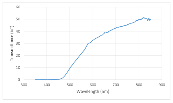 | Figure 6. Optical transmission spectrum of about 1.6 µm thick Cu2O film deposited on glass coated with FTO |
For the determination of the optical band gap energy  equation (4) was used, where the value of
  was found to be 1 (which corresponds to direct band to band transition) because that value of
  yields the best linear graph of
  versus
  . The absorption coefficient and transmittance were calculated using equations (5) and (6) respectively.Figure 7 shows
  versus
  dependence for the Cu2O/FTO film (Tauc plot).
 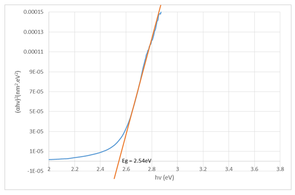 | Figure 7. Graphical determination of the optical band gap energy for Cu2O/FTO thin film (Tauc plot) |
The intersection of the straight line with the  determines the optical band gap energy
  It was found to be 2.54eV for the deposited Cu2O/FTO. It is higher than the value of 2.0 eV given in the literature and obtained for Cu2O polycrystals. This may be as a result of some variations in deposition voltage experienced during the course of deposition, because band-gap energy has been shown to be affected by solution pH and deposition voltage. While we are sure we had a pretty constant solution pH, the same cannot be said for the voltage because we experienced some helpless technical issues at some point during deposition. But generally, annealing does not affect the band-gap energy of electrodeposited Cu2O films.
4.5. Current-Voltage Characterization (Solar Simulation)
In order to compare the performance and the effect of annealing on the current-voltage characteristic of the cuprous oxide solar cell, one of the cells deposited was not annealed, and thus the data obtained from tests conducted on this cell was compared with those from annealed samples. Figure 8 shows the solar cell I-V characteristic of the annealed sample under illumination in the first quadrant. 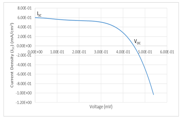 | Figure 8. Current-Voltage (I-V) Characterisation of electro-deposited Cu2O film on FTO glass substrate |
From the figure, a short-circuit current density of  was obtained at V=0, while at open-circuit conditions, I = 0, an open circuit voltage of
  was measured. But
  depends on the saturation current of the solar cell and the light-generated current. Silicon solar cells on high quality single crystalline material have open-circuit voltages of up to 730mV under one sun and AM1.5 conditions, while commercial devices on multi-crystalline silicon typically have open-circuit voltages around 600mV. Similarly, Silicon solar cells under an AM1.5 spectrum have a maximum possible current of
  Laboratory devices have measured short-circuit currents of over
  , and commercial solar cells have short-circuit currents between
  and 35 mA/cm2 [20-21]. The determination of the characteristic parameters under illumination is straightforward, and the results are shown in Table 1.
Table 1. Experimentally obtained characteristics parameters of the Cu2O solar cell under illumination
 |
| |
|
From Figure 9, the maximum power of 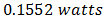 was recorded. Meanwhile, a theoretical power of
  was obtained. The fill factor was calculated using equation (7) and the efficiency was evaluated using equation (8). A fill factor value of 0.571 was recorded, while an efficiency of 0.058% was obtained. But variation in FF can be significant for solar cells made from different materials. For example, a GaAs solar cell may have a FF approaching 0.89, while a silicon laboratory device and a typical commercial solar cell will give maximum FF’s of 0.85 and 0.83 respectively [21]. A designated illumination area of a silicon solar cell with an area of 4.0cm2 designed by UNSW (University of New South Wales), was reported to have an efficiency of 25%, a
  of 0.706V,
  of 42.70mA/cm2, and a FF of 82.80% ([21]).
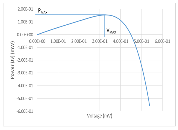 | Figure 9. Power-Voltage (P-V) Characterisation of electro-deposited Cu2O film on FTO |
5. Conclusions
A p-n homojunction cuprous oxide was successfully deposited on an FTO glass substrate, and from analyses conducted on the cell, cuprous oxide exhibited outstanding structural and optical characteristics as well as good electrical features. The overall performance of the cell indicates its great potential for application in photovoltaic devices. Values of  ,
,  ,
,  ,
,  ,
,  ,
,  0.571 and 0.058% were recorded for the short-circuit current density (
 ), open-circuit voltage (
 ), theoretical power (
 ), maximum power (
 ), maximum voltage (
 ), maximum current
  fill factor (FF), and efficiency respectively. Although the resistance of the cell was still high as observed, but efforts are already ongoing to overcome this challenge. One of the most promising solutions of the researches thus far is doping both the p-Cu2O and n-Cu2O with appropriate dopants.
References
| [1] | Ohajianya, A. C., & Abumere, O. E. (2013). Effect Of Cuprous Oxide (Cu2O) Film Thickness On The Efficiency Of The Copper-Cuprous Oxide (Cu2O/Cu) Solar Cell. The International Journal Of Engineering and Science (IJES), 42-47. |
| [2] | Bugarinović, S., Rajčić-Vujasinović, M., Stević, Z., & Grekulović, V. (2014, March 14). InTech Europe. Retrieved from InTech Web site: https://soso.bz/jq9wOVk3Tj. |
| [3] | Wang, L., Han, K., Han, X., & Tao, M. (2008). P-n junction from Solution: Cuprous oxide p-n Homojunction by Electrodeposition. IEEE, 2-6. |
| [4] | Dubey, S., Jadhav, N. Y., & Zakirova, B. (2013). Socio-Economic and Environmental Impacts of Silicon Based Photovoltaic (PV) Technologies. Energy Procedia, 322 – 334. |
| [5] | Rahman, S. A., Islam, M. A., & Shorowordi, K. M. (2015 ). Electrodeposition and Characterization of Copper Oxide Thin Films for Solar Cells Application. 6th BSME International Conference on Thermal Engineering (ICTE 2014) (pp. 679–685). Bangladesh: Elsevier. |
| [6] | Georgieva, V., Tanusevski, A., & Georgieva, M. (2012, June 6). InTech Europe. Retrieved from InTech website: https://soso.bz/Jh6YT5zn0g. |
| [7] | Rakhshani, A. E., Al-Jassar, A. A., & Varghese, J. (1987). Electrodeposition and Charaterization of Cuprous oxide. Thin Solid films, 191-201. |
| [8] | Mukhopadhyay, A. K., Chakraborty, A. K., Chatterjee, A. P., & Lahiri, S. K. (1992). Galvanostatic Deposition and Electrical Characterization of Cuprous Oxide Thin Films. Thin solid films, 92-96. |
| [9] | Golden, T. D., Shumsky, M. G., Zhou, Y., VanderWerf, R. A., Van Leeuwen, R. A., & Switzer, J. A. (1996). Electrochemical Deposition of Copper(I) Oxide Films. Chem. Mater., 2499-2504. |
| [10] | Chen, L., Shet, S., Tang, H., Wang, H., Deutsch, T., Yan, Y. and Al-Jassim, M. (2010). Electrochemical Deposition of Copper Oxide Nanowires for Photoelectrochemical Applications. Journal of Materials Chemistry, 6962-6967. |
| [11] | Wijesundera, R. P. (2014, March 15). InTech Europe. Retrieved from InTech website: https://soso.bz/1RkRl9wPe4. |
| [12] | Wong, T. K., Zhuk, S., Masudy-Panah, S., & Dalapati, G. K. (2016). Current Status and Future Prospects of Copper Oxide Heterojunction Solar Cells. Materials, 1-21. |
| [13] | Perera, L. R., Siripala, W., & De Silva, K. L. (1996). Potentiostatic Electrodeposition of Cuprous Oxide Thin Films. J. Natn. Scien. Coun., 299-308. |
| [14] | Wang, L., & Tao, M. (2007). Fabrication and Characterization of p-n Homojunctions in Cuprous Oxide by Electrochemical Deposition. Electrochemical and Solid-State Letters, H248-H250. |
| [15] | Han, K. and Tao, M. (2009). Electrochemically Deposited p-n Homojunction Cuprous oxide Solar Cells. Solar Energy Materials and Solar Cells, 153-157. |
| [16] | Han, K. (2009). Electrodeposited Cuprous Oxide Solar Cells. Arlington: Univrersity of Texas. |
| [17] | Septina, W., Ikeda, S., Alam Khan, M., Hirai, T., Harada, T., Matsumura, M., & Peter, L. M. (2011). Potentiostatic Electrodeposition of Cuprous Oxide Thin Films for Photovoltaic Applications. Electrochimica Acta, 4882–4888. |
| [18] | McShane, C. M., & Choi, K.-S. (2012 ). Junction Studies on Electrochemically Fabricated p–n Cu2O Homojunction Solar Cells for Efficiency Enhancement. Phys. Chem. Chem. Phys., 6112–6118. |
| [19] | Wang, L. (2006). Preparation and Characterisaion of Properties of Electrodeposited Copper Oxide Films. Arlington: University of Texas at Arlington. |
| [20] | Alsubaie, M. (2013). Characterisation of Photovoltaic Module. Manchester: Manchester Metropolitan University |
| [21] | Honsberg, C., & Bowden, S. (2017, August 8). PVEDUCATION.ORG. Retrieved from Open-Circuit Voltage-PVEducation: http://www.pveducation.org/pvcdrom/short-circuit-current. |

 Abstract
 Reference
 Full-Text PDF
 Full-text HTML