-
Paper Information
- Paper Submission
-
Journal Information
- About This Journal
- Editorial Board
- Current Issue
- Archive
- Author Guidelines
- Contact Us
Electrical and Electronic Engineering
p-ISSN: 2162-9455 e-ISSN: 2162-8459
2020; 10(1): 15-22
doi:10.5923/j.eee.20201001.03

Energy Consumption of a Sub-threshold Analog Signed Multiplier Compared to a Digital Implementation
 Abstract
 Reference
 Full-Text PDF
 Full-text HTML
Grant S. Christiansen, Gary S. Delp, Barry K. Gilbert
Special Purpose Processor Development Group, Mayo Clinic, Rochester, Minn, USA
Correspondence to: Grant S. Christiansen, Special Purpose Processor Development Group, Mayo Clinic, Rochester, Minn, USA.
| Email: |  |
Copyright © 2020 The Author(s). Published by Scientific & Academic Publishing.
This work is licensed under the Creative Commons Attribution International License (CC BY).
http://creativecommons.org/licenses/by/4.0/

We compare the energy consumed by 8-bit x 8-bit and 16-bit x 16-bit multipliers composed of small analog multipliers implemented using transistors operating in their sub-threshold regions to the energy consumed by equivalent digital implementations. The analysis shows that the analog energy consumption is determined by the required signal-to-noise ratio of the individual analog multipliers and that the energy consumption is higher than the equivalent digital implementation’s energy consumption.
Keywords: Analog computing, Sub-threshold design, Energy efficiency
Cite this paper: Grant S. Christiansen, Gary S. Delp, Barry K. Gilbert, Energy Consumption of a Sub-threshold Analog Signed Multiplier Compared to a Digital Implementation, Electrical and Electronic Engineering, Vol. 10 No. 1, 2020, pp. 15-22. doi: 10.5923/j.eee.20201001.03.
Article Outline
1. Introduction
- Analog computing, which uses electrical circuits with continuous signals to perform mathematical operations, differs from digital computing in that quantities are represented as signal levels continuously varying over time as opposed to numeric (two-level binary) quantized representations that are sampled over time. Information in analog signals can be stored and transferred in many forms, including voltage levels, current flow, frequencies, or phase-shifted waves.Analog computing, using transistors in their sub-threshold region of operation, has shown energy consumption advantages in inexact applications, where precise answers are not required (e.g., speech recognition [1], solving differential equations [2]). Given those successes in inexact computing, it appears worth considering whether those energy advantages could be applied to precise mathematical computations consisting of exact multiplications and additions.As an indicator to whether analog computations can be more energy efficient than digital computations, we consider the energy consumption of an analog signed multiplier using transistors operating in their sub-threshold region, and compare it to the energy consumption of a signed digital multiplier (as would be available in commonly available microprocessors), both implemented in state-of-the-art CMOS technology. The layout of the paper is as follows.In section 2 we analyze the energy consumption of a signed analog multiplier. In section 3 we anayze the energy consumption of an equivalent digital signed multiplier. In section 4 we compare the two types of multipliers and present our conclusions.
2. Analog Multiplier Analysis
2.1. Analog Design Challenges
- Challenges with analog circuitry include, e.g., signal linearity, sensitivity to noise, transistor mismatch, drift, component tolerances, and offset and gain variation with temperature, process, and supply. Adding compensation circuitry may increase energy consumption.1To attempt to address the transistor mismatch and tolerance concerns, this paper will examine an analog implementation of signed multipliers using floating-gate transistors, described in the next section. We also will use transistors in their sub-threshold region, which has the promise of lower power consumption and improved linearity of the multiplier circuit compared to using transistors in their active region.
2.2. Sub-Threshold Design and Floating Gate Design
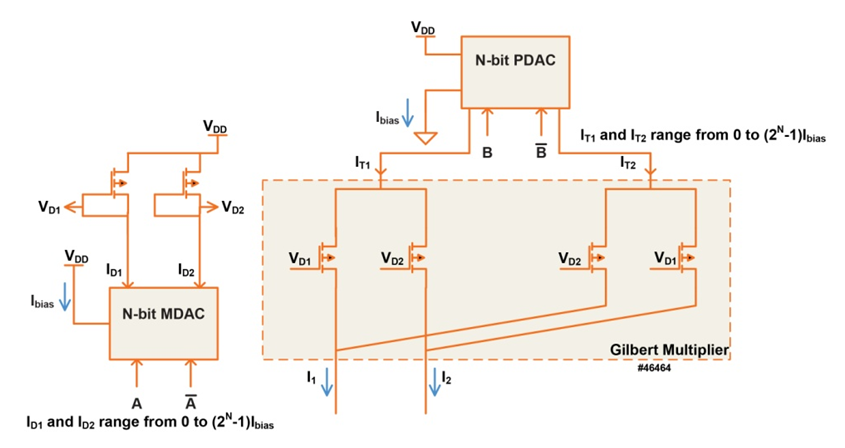
- Traditionally analog circuitry is designed using transistors biased into their “active” region. One idea to reduce power consumption is to construct circuits biased in their “sub-threshold” region. However, “sub-threshold” designs suffer from degraded transistor-to-transistor matching and noise performance (since the circuit current magnitudes would be less) compared to “active” designs.Two techniques have been suggested to improve matching in sub-threshold designs: adaptive body biasing (ABB) [3] and the use of floating gate (FG) transistors [4]. In ABB, additional circuitry is added to measure and compensate for any mismatches. Since the additional circuitry would add to the power consumption, we decided to focus on the second, floating gate, method, which does not have the power penalty of adaptive circuitry.A “floating gate” transistor is a FET manufactured so its gate terminal is insulated from the rest of the transistor, forming a gate that, while “floating” from the transistor channel, is capacitively coupled to it. Additional capacitors are added to the structure to allow for connection to a circuit (isolating the programmed floating gate from the rest of the circuit) for programming. Programming injects or removes charge on the floating gate, which causes a change in the effective threshold voltage. The result is that any variance in the threshold voltages can be minimized by injecting or removing charge on the floating gate [5].
2.3. High-Level Analog Multiplier Architecture
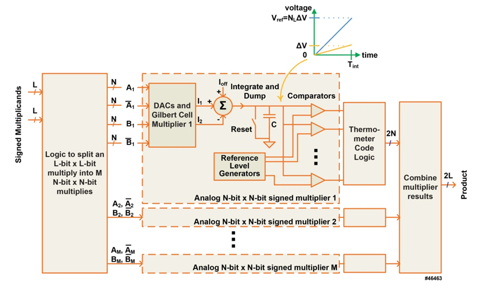
- One challenge of analog computing is the very wide dynamic range needed to represent numbers made up of only a small number of bits. Representing a 16-bit number, for example, as an analog voltage between zero and 5 volts requires a resolution of 76 µV. Fortunately, there are techniques (e.g., breaking the problem down into smaller segments with fewer bits each using residue number systems for the calculations) that allow a higher resolution result to be built up from the results of many lower-resolution calculations; it is therefore possible to use multiple analog circuits of reasonable resolutions. Figure 1 shows a possible design of an L-bit by L-bit signed multiplier (producing a result of width 2L bits) that addresses the resolution challenge by decomposing it into M N-bit x N-bit signed multipliers implemented as Gilbert-cell multipliers [6].The logic block at the left side of Figure 1 splits the larger L-bit x L-bit problem into several smaller problems that are inputs to the analog signed multiplier blocks. The output of the analog block is a thermometer code that is resolved and combined with the results of the other analog multipliers in the logic blocks at the right of the figure.
 | Figure 1. Analog Implementation of an L-bit x L-bit Signed Multiplier |
 | (1) |
2.4. Analog Multiplier Implementation
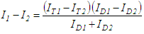
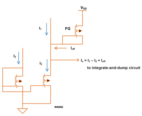
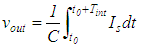
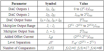
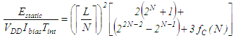
- The analog signed multipliers each consist of a Gilbert cell multiplier and supporting DACs that produce a differential current, I1 – I2, representing the signed multiplication of two N-bit values. An offset current, Ioff, is added to the differential current to make the current into the subsequent integrate-and-dump circuit unipolar. The integration time is denoted Tint. The result of the integration, a voltage that ranges from 0 volts to Vref, is passed to several comparators to determine the final multiplication result. The number of comparators is a function of the size of the multiplier and is referred to as fc(N) in the equations below. The minimum voltage size difference between output levels is ΔV, which appears prominently in the signal-to-noise calculations.The Gilbert cell multiplier block, including DACs at the front end, is shown in Figure 2. A Gilbert cell was chosen to implement the multiplication because transistors in their sub-threshold region have characteristics that give a very linear response to current inputs to the cell [7]:
 | (2) |
 | Figure 2. Gilbert Cell Multiplier with DACs |
 | Figure 3. Example of a 3-bit MDAC and PDAC using Floating Gate Transistors to Set the Bias Current |
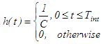
 | Figure 4. Circuitry Creating Unipolar Current into the Integrate-and-Dump |
 | (3) |
|
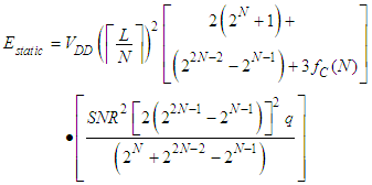
2.5. Analog Multiplier Energy Consumption
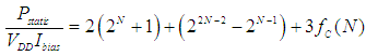
- The static power consumption of the N-bit x N-bit analog multiplier is the power supply voltage multiplied by the current that it draws from the supply. The supply currents include (1) the MDAC and PDAC currents, (2) the added offset current, (3) the currents from the reference level generators, and (4) the currents from the comparators.
 | (4) |
 | (5) |
2.6. Signal to Noise Ratio Analysis
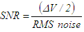
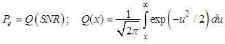
- The output of the integrate-and-dump circuit feeds comparators with a minimum difference between levels of ΔV. That means that a signal deviation from the ideal levels of ΔV/2 will cause an error in the multiplication, so we define the SNR voltage ratio as (where ΔV is defined in Table 1):
 | (6) |
 | (7) |
 | (8) |
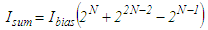 | (9) |
 | (10) |
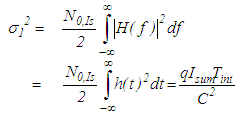 | (11) |
 | (12) |
 | (13) |
 | (14) |
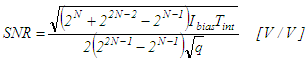 | (15) |
 | (16) |
 | (17) |
2.7. Flicker Noise Considerations
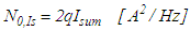
- The signal-to-noise calculations in section 2.6 neglect the effects of flicker noise, which can be a significant noise contributor in CMOS circuits. Because the magnitude of flicker noise depends on the CMOS transistor geometry (flicker noise reduces as channel length and widths are increased [17]), the amount of flicker noise could in principle be reduced to be less than the thermal and shot noises if the area penalty were acceptable. Thermal and shot noise terms cannot be reduced by changing transistor geometries and so the ultimate circuit performance is limited by the SNR determined in section 2.6.
2.8. Static Energy Calculation Results
- Figure 5 shows both the static energy required for 8-bit x 8-bit and 16-bit x 16-bit multiplies using smaller analog multipliers with N=2, 3, and 4 as a function of operation error rate as well as the energy with N=2 (the most promising data) under the assumption that VDD=0.7 volts, which is reasonable for a state-of-the-art technology.
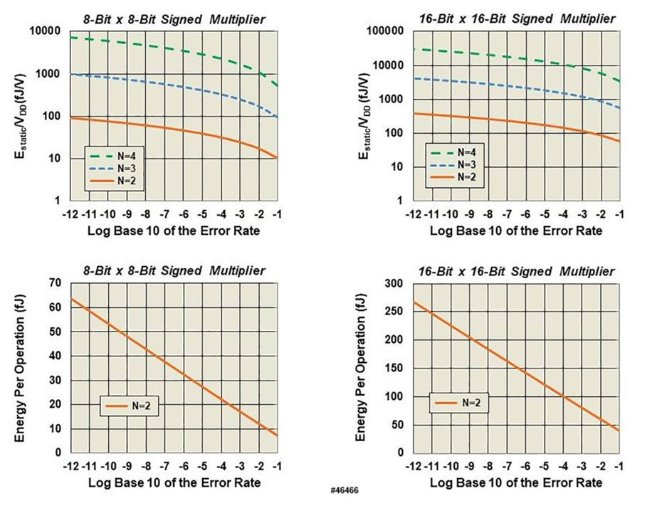 | Figure 5. Normalized Analog Energy and Energy Consumption at VDD=0.7 volts (Note: as expected, E16x16 ≈4*E8x8) |
3. Digital Implementation Comparison
3.1. Digital Implementation
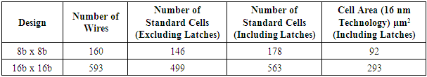
- In this portion of the paper we estimate the static and dynamic power and energy consumption of digital multipliers implemented in a state-of-the-art technology to act as a benchmark with which to compare the energy consumption results of the analog multipliers. We concentrate on the characteristics of two signed multipliers: an 8-bit x 8-bit (producing a 16-bit result) and a 16-bit x 16-bit (producing a 32-bit result).The methodology was to write a high-level description of the multipliers in VHDL and allow a synthesis tool [9] to create a “vanilla” implementation of the two multipliers using a state-of-the-art standard-cell library. No special care was taken to optimize the multipliers for power. The library included half- and full-adder cells, and the implementation took advantage of these (Figure 6, Table 2).
|
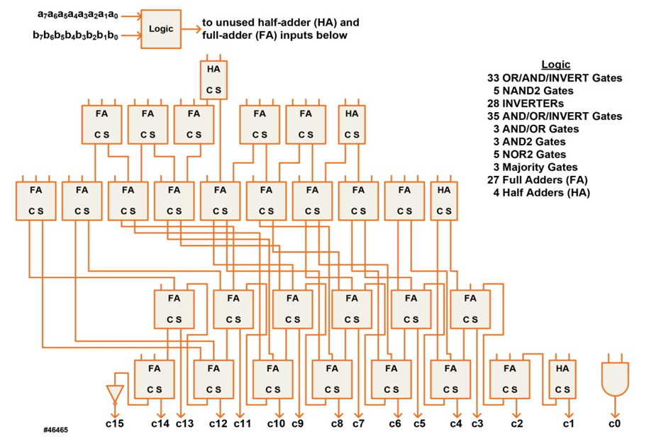 | Figure 6. Implementation of a Digital 8-bit x 8-bit Signed Multiplier |
3.2. Dynamic Power Estimation
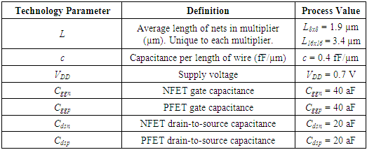
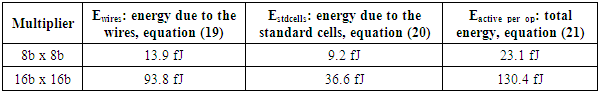
- Active CMOS energy consumption can be divided into two portions: (1) the energy consumption of nets (traces) between standard cells and (2) the energy consumption of the standard cells themselves, including energy to charge any FETs connected to input and output nets. The energy consumption depends on the technology characteristics listed in Table 3, which includes assumed values for a state-of-the-art (e.g., 7 nm) technology.The average net length was determined by first using data from [10], which estimates that an average net in a design is 40% of the length of the side of square layout for approximately the number of cells in our designs. Applying a scaling factor of ¼ to the area when going from 16 nm to 7 nm [11] gives the values in Table 3.
|
 | (18) |
 | (19) |
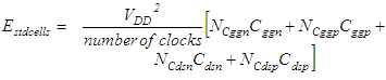 | (20) |
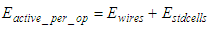 | (21) |
|
3.3. Static Power Estimation
- Due to leakage current in the FET devices, CMOS circuits consume power even when not switching, which is called static power. [16] estimates a 16-bit x 16-bit multiplier operating at a supply voltage of 0.45 volts to have a leakage power of 1.82 microwatts. Scaling the power supply voltage to 0.7 volts gives 2.8 microwatts of static power.Since leakage power is proportional to the number of transistors in a circuit, we estimate the 8-bit x 8-bit multiplier power as 178/563 (Table II) of the 16-bit x 16-bit multiplier, or 0.9 microwatts.
3.4. Total Energy per Operation Estimation
- The total energy per operation depends on the clock speed f:
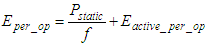 | (22) |
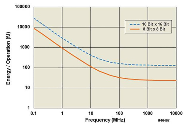 | Figure 7. Total Energy per Operation for Digital Signed Multipliers |
4. Discussion and Conclusions
- For the digital implementation of the 8-bit x 8-bit and 16-bit x 16-bit multipliers, Figure 7 indicates that the energy consumption per multiplication operation is dominated by the dynamic energy consumption for operating frequencies greater than 100 megahertz, which is certainly reasonable. That means that the energy consumption benchmark is the “Eactive_per_op” column of Table 4.A comparison of these energy consumption values against Figure 5 shows that the analog circuitry energy consumption is higher than the equivalent digital circuit energy consumption unless the system error rate is allowed to be about 1 error in 105 multiply operations.The analog energy consumption is independent of the bias current, and is instead proportional to the bias current multiplied by the integration time. This may not be surprising, since the product of the bias current, the power supply voltage, and the integration time has units of energy. The analog circuit energy consumption was determined by and was directly related to the square of the (voltage/voltage) signal-to-noise ratio, and so it quickly increased as the number of bits in the analog multiplier was increased. The most efficient decomposition of the large multiplier was to use the smallest analog multiplier.The analysis of the analog multiplier was optimistic; it assumed that flicker noise could be reduced to a negligible level through transistor scaling and did not consider the energy consumption of additional circuitry that might be needed to compensate for temperature drift. The analysis also did not include the energy consumption of the digital logic surrounding the analog computation core.It may be that the Gilbert cell multiplier is not the most power efficient analog multiplier. We briefly considered a multiplying DAC implementation, but it appeared to consume more power than the Gilbert cell implementation.
Note
- 1. In this paper we have been careful to distinguish energy from power (energy over time). The static power is amortized over a larger number of operations when the operations/unit time is increased; this can reduce the energy per operation.