-
Paper Information
- Paper Submission
-
Journal Information
- About This Journal
- Editorial Board
- Current Issue
- Archive
- Author Guidelines
- Contact Us
Electrical and Electronic Engineering
p-ISSN: 2162-9455 e-ISSN: 2162-8459
2019; 9(2): 45-52
doi:10.5923/j.eee.20190902.04

PIC32MZ Custom I2C Master Communication API Library
 Abstract
 Reference
 Full-Text PDF
 Full-text HTML
Abhishek N. Patel
Research and Development Department, Horiba Instruments Inc., 20 Knightsbridge Road, Piscataway, New Jersey, United States
Correspondence to: Abhishek N. Patel, Research and Development Department, Horiba Instruments Inc., 20 Knightsbridge Road, Piscataway, New Jersey, United States.
| Email: |  |
Copyright © 2019 The Author(s). Published by Scientific & Academic Publishing.
This work is licensed under the Creative Commons Attribution International License (CC BY).
http://creativecommons.org/licenses/by/4.0/

This paper demonstrates how to make I2C master communication library routines for PIC32MZ/PIC32 MCUs. I2C is a synchronous serial communication protocol. It provides the good support for communication with slow peripheral devices such as EEPROM, ADC, RTC, Voltage Monitor etc. Unfortunately, the microchip PICXC32 compiler does not gives us the I2C library APIs to call from firmware application layer. This implementation requires PIC32MZ/PIC32 MCU based hardware and microchip MPLAB-X IDE, tool chain and Harmony framework.
Keywords: C, PIC32MZ, PIC32, Firmware, Embedded System, i2C
Cite this paper: Abhishek N. Patel, PIC32MZ Custom I2C Master Communication API Library, Electrical and Electronic Engineering, Vol. 9 No. 2, 2019, pp. 45-52. doi: 10.5923/j.eee.20190902.04.
Article Outline
1. Introduction
- The I2C-bus developed by Philips to maximize hardware efficiency and circuit simplicity. The I2C interface is a simple master/slave type interface. In I2C, both buses are bidirectional, which means master able to send and receive the data from the slave. I2C is a 2-wire design, one wire used for serial data line (SDA) and other one used for serial clock line (SCL). I2C is appropriate for interfacing to devices on a single board. This can be stretch across multiple boards inside a closed system, but not much further. For an example, the PIC MCU on a main embedded board using I2C to communicate with user interface devices located on a separate front panel board. A second example is SDRAM DIMMs, which can feature an I2C EEPROM containing parameters needs to correctly configured a memory controller for that module.
2. I2C Detail
- The two I2C signals are serial data (SDA) and serial clock (SCL). Together, these signals make it possible to support serial.Transmission of 8-bit bytes of data-7-bit device addresses and control bits-over the two-wire serial bus. The lines are open-drain (open-collector). This means that devices on the I2C bus can only pull the line low or leave them open/floating. This means that both SDA and SCL needs a pull-up resistor, otherwise they will not be able to set the lines high.The device that initiates a transaction on the I2C bus is termed the master. The master normally controls the clock signal. A device being addressed by the master is called a slave.In a bind, an I2C slave can hold off the master in the middle of a transaction using what via clock stretching (the slave keeps SCL pulled low until it is ready to continue). Most I2C slave devices do not use this feature, but every master should support it.The I2C protocol supports multiple masters, but most system designs include only one. There may be one or more slaves on the bus. Both masters and slaves can receive and transmit data bytes.Each I2C-compatible hardware slave device comes with a predefined device address, the lower bits of which may be configurable at the board level. The master transmits the device address of the intended slave at the beginning of every transaction. Each slave is responsible for monitoring the bus and responding only to its own address.
2.1. I2C Protocol Overview
- Both SDA and SCL are bidirectional communication signals and can be change by either master or slave. SDA is the Serial data line, and SCL is the Serial clock line. Every device hooked up to the bus has its own unique address, no matter whether it is an MCU, LCD driver, EEPROM memory, or ASIC. Each of these chips can act as a receiver and/or transmitter, depending on the functionality. Obviously, an LCD driver is only a receiver, while an EEPROM memory or I/O chip can be both transmitter and receiver.The I2C bus is a multi-master bus. This means that more than one IC capable of initiating a data transfer and could be connected to it. The I2C protocol specification states that the IC that initiates a data transfer on the bus and considered the Bus Master, which generally is a microcontroller (PIC32MZ for this article). Consequently, at that time, all the other ICs considered to be as a Bus Slaves.First, the MCU will issue a START condition. This acts as an 'Attention' signal to all of the connected devices. All ICs on the bus will listen to the bus for incoming data.Then the MCU sends the ADDRESS of the device it wants to access, along with an indication whether the access is a Read or Write operation. Having received the address, all IC's will compare it with their own address. If it does not match, they simply wait until the bus is released by the stop condition. If the address matches, however, the chip will produce a response called the ACKNOWLEDGEMENT signal.Once the MCU receives the acknowledgement, it can start transmitting or receiving DATA. When it complete the trasaction, the MCU will issue the STOP condition. This is a signal that the bus has been release and that the connected ICs may expect another transmission (DATA transaction) to start any moment.
2.2. I2C Order of Operation
- Unlike UARTs and SPI, I2C employs a handshaking protocol between master and slave. Let us look at two example. In the first, a byte (8-bits) of data is being written to a slave that has an I2C address of 0x50. The slave's internal register number is 0x55 and we want to set it to a value of 0x11.The order of operations would be:• Send start signal• Write slave address with Read/Write bit set to 0 (Send 0x50 << 1 = 0xA0)• Receive ACK• Write register address (0x55)• Receive ACK• Write data value (0x11)• Send stop signalThat second line is going to be confusing. Take a look again at how the 9-bit number is made up above. We are actually only sending 8 bits, the ACK is automatic so let's look at the first 8 bits. The upper 7 bits contain the slave's address and the least significant bit is the R/W bit. This means that 7-bit I2C addresses need to be shifted left by 1 when writing them to the I2C bus.For the second example, 8 bits of data will be read from the same slave, register number 0x72.The order of operations would be:• Send start signal• Write slave address with Read/Write bit set to 1 (Send 0x50 << 1 | 1 = 0xA1)• Receive ACK• Write register address (0x72)• Receive ACK• Receive data byte (8-bits)• Send NACK• Send stop signalAgain, that second line. If we want to set the least significant bit, we can either add 1 to the address or “OR” it by 1, which I prefer because it looks more confusing. To receive 8-bit data, send NACK instead of ACK. If we send an ACK, the slave device will start sending me more data.
3. Detail of PIC32MZ I2C Master API/Routines
- The 144-pin PIC32MZ device has five I2C peripherals, which control through seven SFRs. Many of the fields in these SFRs initiate an “event” on the I2C bus. All bits default to zero except I2CxCON.SCLREL. In the SFRs below, x refers to the I2C peripheral number, 1, 3, 4, or 5. The following registers are used:• I2CxCON - I2Cx Control Register - Used to set up I2C peripheral “x”• I2CxBRG - I2Cx Baud Rate Generator Register - Used for setting the speed of the I2C peripheral “x”• I2CxTRN - I2Cx Transmit Data Register - Contains data we want to send onto the I2C bus for peripheral “x”• I2CxRCV - I2Cx Receive Data Register - Contains data received from the I2C bus for peripheral “x”• I2CxADD - I2Cx Peripheral Address Register - Contains I2Cx peripheral slave address (Only for the Slave Mode). • I2CxSTAT - I2Cx Status Register - Contains the status of the I2C peripheral “x”For example to configure I2C peripheral “1” as a master, we need to consider I2C1Con, I2C1BRG, I2C1TRN, I2C1RCV and I2C1STAT registers. This means the two physical pins we will connect to are SDA1 (on port RA15) and SCL1 (on port RA14).
3.1. Configure the Speed of the I2C Peripheral 1 via I2C1BRG Register
- As per the PIC32MZ product page we can run from 100kHz to 1Mhz, the lower 16 bits of I2CxBRG register determine the baud. Typically, the baud is either 100 kHz or 400 kHz. To compute the value of I2CxBRG, use the formula:
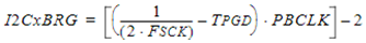 Where Fsck is the desired baud (i.e. 100kHz), Fpb is the peripheral bus clock frequency, and TPGD is 104 ns, according to the Reference Manual. With a 100MHz peripheral bus clock, I2C1BRG = 487 for 100 kHz. Only masters need to set a baud rate. Implement the code to do that:
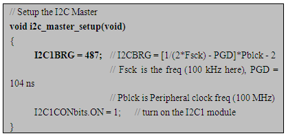
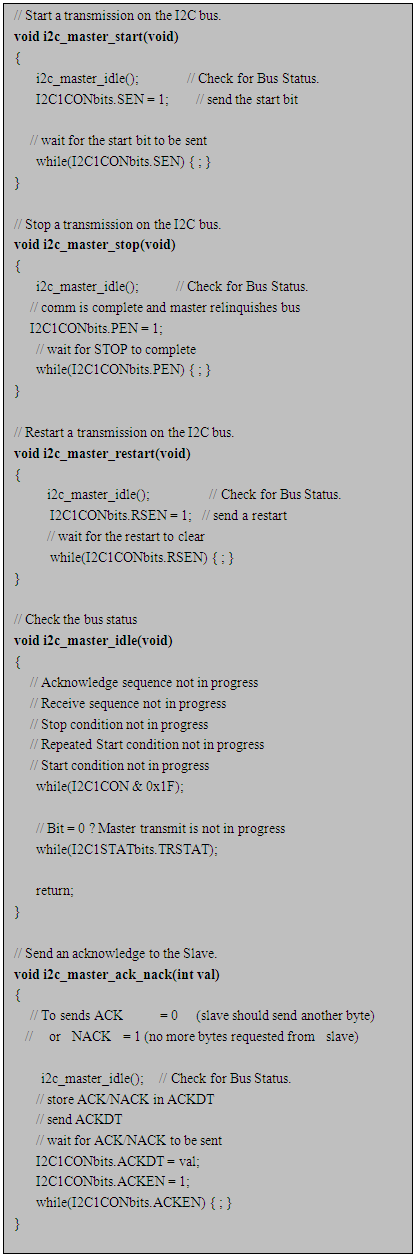
3.2. Create I2C Master Start, Stop, Restart, ACK and NACK API
- The implementation of the I2C master contains functions roughly corresponding to the primitives discussed earlier. Each function executes the primitive command and waits for it to complete. By calling the primitive functions in succession, you can form an I2C transaction. The I2C1CON register mainly used to perform all of these:• I2C1CONbits.SEN - Start Condition Enable bit• I2C1CONbits.PEN - Stop Condition Enable bit• I2C1CONbits.RSEN - Restart (Repeated start) Condition Enable bit• I2C1CONbits.ACKDT - Acknowledge Data bit. Set to 0 to ACK and 1 for NACK.• I2C1CONbits.ACKEN - Acknowledge Sequence Enable bitThe Library API routine code:
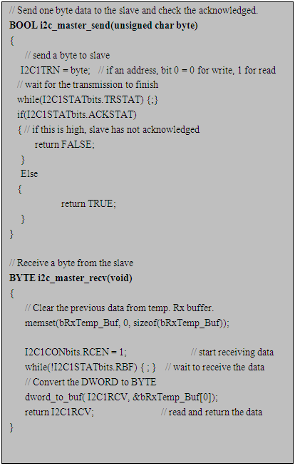
3.3. Create I2C Master Send and Receive Data API
- The I2C1TRN register handles sending data functionality, which is a matter of writing to it and waiting for the Transmit Buffer to be empty by checking Transmit Buffer Full (TBF) flag. After that waiting for the slave device to Acknowledge receipt.For receiving data, wait for it to clear the flag and until the receive buffer is full by checking Receive Buffer Full (RBF) flag and then send either an ACK or a NACK.
4. I2C Master Lib API Real World Usages to Interface with EEPROM Memory
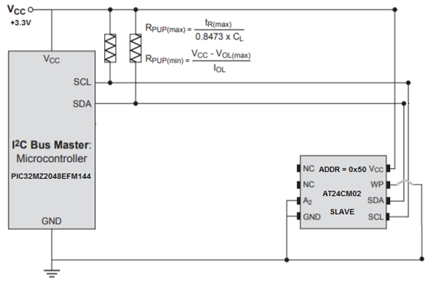
- This section describe application of I2C master library APIs to interface with EEPROM memory via I2C communication bus from PIC32MZ MCU. EEPROM stands for Electrically Erasable Programmable Read-Only Memory. It is a type of non-volatile memory that can be used to store little bits of data. Data will remain on EEPROM when power is disconnected, (like an external hardrive). The EEPROM chip has a life span in the tens or hundreds of thousands of read/writes. This code based on PIC32MZ (act as the I2C Master) and AT24CM02 EEPROM (act as the I2C slave) which communicating via I2C Bus.The Microchip AT24CM02 is a 2Mb Serial EEPROM utilizing an I2C (2-wire) serial interface. The device is an organized as one block of 256K x 8 and is an optimized for use in consumer and industrial applications (such as a spectroscopy configuration and experiment data storage) where reliable and dependable nonvolatile memory storage is essential.
4.1. AT24CM02 EEPROM Device Configuration
- The descriptions of AT24CM02 EEPROM pins are as below:PIN1: No ConnectPIN2: No Connect PIN3: Device Address InputPIN4: Ground PIN5: Serial Data (SDA) LinePIN6: Serial Clock (SCL) LinePIN7: Write ProtectPIN8: Device Power SupplyPIN3 Device Address Input (A2): The A2 pin is a device address input that is hard-wired (directly to GND or to VCC) for compatibility with other two-wire Serial EEPROM devices. Connected it to Ground for configure device address to “0x51”.PIN4 Ground (GND): The ground reference for the power supply and it connected to the system ground.PIN5 SDA: The SDA pin is an open-drain bidirectional input/output pin used to serially transfer data to and from the device. The SDA pin must be pulled high using an external pull-up resistor (not to exceed 10 kΩ in value i.e. 3.3 kΩ) and may be wired with any number of other open-drain or open-collector pins from other devices on the same bus.PIN6 SCL: It provides a clock to the device, which control the flow of data to and from the device. Command and input data present on the SDA pin is always latched in on the rising edge of SCL, while output data on the SDA pin is clocked out on the falling edge of SCL. The SCL pin must either be forced high when the serial bus is idle or pulled high using an external pull-up resistor.PIN7 WP: The write-protect input is connected to GND, allows normal write operations. PIN8 VCC: The VCC pin used to supply the source voltage to the device (+3.3 volt).The PIC32MZ2048EFM144 MCU configuration using 2-wire serial EEPROM.
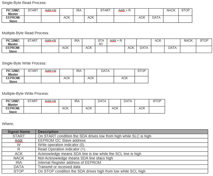
4.2. Read and Write Cycle Process
- Read operations are initiated the same way as write operations with the exception that the Read/Write Select bit in the device address byte must be a logic ‘1’. There are three read operations: - Current Address Read - Random Address Read - Sequential ReadAll write operations for the AT24CM02 begin with the master sending a Start condition, followed by a device address byte with the R/W bit set to logic ‘0’, and then by the word address bytes. The data value(s) to be written to the device immediately follow the word address bytes. It support two write mode.- Single Byte write mode.- Whole page of 256 bytes write mode.Refer the sequential flow of read and write operations:
4.3. Write Cycle Time
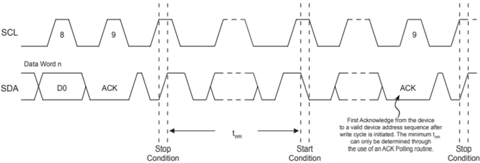
- The length of the self-timed write cycle (tWR) defined as the amount of time from the Stop condition that begins the internal write cycle to the Start condition of the first device address byte sent to the AT24CM02 that it subsequently responds to with an ACK. During the internally self-timed write cycle, any attempts to read from or write to the memory array will not be processed.The default Write Cycle time is 10 milliseconds for AT24CM02 EEPROM, this could be implemented using “delay_ms()” routine. (The Delay Millisecond routine API Corresponding citation: (Patel, 2019))
4.4. Code for PIC32MZ and AT24CM02 EEPROM Communication over I2C Bus
- This sample code design to read and validate the serial number from AT24CM02 EEPROM using I2C master library API. Also validate the serial number, it restore to default in case it is an invalid serial number. Similar to the serial number there are more data which stored into AT24CM02 EEPROM (such as a spectroscopy instrument configuration for performing an experiment, error log, event log, correction angle data points, manufacturing information, factory default instrument configuration etc.).

5. Conclusions
- These costume I2C master Library APIs can be useful for any PIC32 embedded system based project. There could be a numerous condition in real world applications where we need this I2C Master Library APIs to communicate with MCU, LCD driver, EEPROM memory, ASIC, voltage and temperature monitor chip via I2C communication bus from PIC32 MCU. These I2C Master Library APIs implemented successfully using PIC32MZ MCU hardware and MPLAB software stack that includes MPLAB X IDE, Tool chain and Harmony framework. The above example of storing and retrieving a serial number to AT24CM02 EEPROM from PIC32MZ demonstrated usages of via I2C master library APIs.