-
Paper Information
- Paper Submission
-
Journal Information
- About This Journal
- Editorial Board
- Current Issue
- Archive
- Author Guidelines
- Contact Us
Electrical and Electronic Engineering
p-ISSN: 2162-9455 e-ISSN: 2162-8459
2019; 9(1): 17-26
doi:10.5923/j.eee.20190901.03

Development of Ku Compact Broadband 1x4, 1x8 and 1x16 Power Dividers with SIW Optimized Chamfered Bends
 Abstract
 Reference
 Full-Text PDF
 Full-text HTML
Rahali Bouchra, Abdeldjelil Amina
STIC Laboratory, Department of Electrical Engineering, Faculty of Technology, University of Tlemcen, Tlemcen, Algeria
Correspondence to: Rahali Bouchra, STIC Laboratory, Department of Electrical Engineering, Faculty of Technology, University of Tlemcen, Tlemcen, Algeria.
| Email: |  |
Copyright © 2019 The Author(s). Published by Scientific & Academic Publishing.
This work is licensed under the Creative Commons Attribution International License (CC BY).
http://creativecommons.org/licenses/by/4.0/

In this paper, compact broadband 1×4, 1×8 and 1x16 SIW power dividers based on SIW chamfered right bend operating in Ku-band frequency and that provide equal power split in all output ports are presented. Substrate Integrated Waveguide is an artificial waveguide synthesized and constructed with linear arrays of metalized via-holes in the same substrate used for the planar circuit. In this paper SIW H plane chamfered right bend and dividers are simulated and optimized using 3D FEM simulator HFSS, also the frequency responses as the return losses, transmission coefficients and the field’s distribution are exposed. The concept is validated by simulations using CST Microwave Studio. These broadband SIW power dividers can be used widely in microwave and millimeter-wave circuits and system.
Keywords: Substrate integrated waveguide, Bend, Chamfered, Power divider, HFSS, CST
Cite this paper: Rahali Bouchra, Abdeldjelil Amina, Development of Ku Compact Broadband 1x4, 1x8 and 1x16 Power Dividers with SIW Optimized Chamfered Bends, Electrical and Electronic Engineering, Vol. 9 No. 1, 2019, pp. 17-26. doi: 10.5923/j.eee.20190901.03.
Article Outline
1. Introduction
- At high frequencies waveguide devices are preferred; however their manufacturing process is difficult. Therefore a new concept emerged: substrate integrated waveguide [1-3]. A typical SIW structure is constructed by two parallel rows of via holes having diameter d is repeated by a period of p, a substrate with height h and dielectric constant 𝜀r is sandwiched by the top and bottom plates of metal. It is now possible to fully integrate the transition, connecting planar transmission line, and waveguide on the same substrate [4]. Another attractive feature of substrate integrated waveguides is the large bandwidth they provide, as well as at higher microwave and millimeter-wave frequencies. The monomode bandwidth of the first dominant mode of the SIW is from the first cutoff frequency fc1 to approximately 2fc1. This large available pass band at high-frequencies makes the SIW a strong candidate as an interconnect for ultra wideband and high-speed data transmission. By the way, power dividers/combiners [5] are one of the key passive components to construct microwave circuits and subsystems. Power dividers are considered as one of the essential components in microwave systems. Numerous designs of microwave power dividers with various features have been developed. Output matching and isolation of the power dividers are of great importance for achieving the high performance multi-way systems such as antenna array systems by minimizing the mutual coupling between the array elements.Since the SIW technology is still on the research level, it has to bring proof of its potential. In the Ku band [6, 7], all the components of a transmitter are the subject of a design followed by a validation. One of the transceiver component is the antenna feed network. For certain types of antennas this circuit can be a power divider.The main objective of this paper is the design of a 1 to 16 SIW power divider that can feed from a single input power a 16-port network antenna with equal amplitude and phase.In this paper, Ku-band 1×4, 1×8 and 1x16 SIW power dividers junction designed from SIW chamfered right bend [6, 8], operating in the range frequency [12-18] GHz, are proposed and analyzed using 3D simulator HFSS software [9]. The obtained results are validated with those given by the CST Microwave Studio (MWS) [10].The work of this paper is organized as follows. Optimized SIW chamfered bends are developed in Sect. 2. SIW T- junction with inductive post is given in Sect. 3. Validation and Simulation results of 1x4, 1x8 and 1x16 power dividers are presented in Sect. 4. Finally, conclusions are drawn in Sect. 5.
2. Optimized SIW Chamfered Bends
- The rectangular waveguide bends are extensively used in many microwave components such as wave transformers, power dividers, radar seekers, satellite beam forming networks. It is thus interesting to implement H plane corners in the form of SIW technology Figure 1a that have high performance rectangular waveguide components and can be integrated at low cost using standard PCB processes. Figure 1b depicts the top view of an H-plane SIW bend with right angle, which is constructed in a Fr4 substrate with dielectric constant εr=4.4 tanζ = 0.02. The width of the Ku band SIW has been determ1ined according to the cutoff frequency obtained from the empirical formulae [3]. The width of the bend is Wsiw=8.54mm, cylinder diameter is d=1.524mm, the cylinder spacing is p=2.54mm, the height of the substrate is H=0.508mm.The common method to compensate the discontinuity of right bend in waveguide is to chamfrain [6] its corner in order to reduce the reflection. In [6] we have analyzed the compensation of the discontinuity of right bend Figure 1 and investigated the influence of the chamfered bends in SIW technology. The chamfrain is useful to reduce the losses at the right bend corner, and the position of the chamfrain depicted by Aopt Figure 1c, Aopt is the distance between the middle of the chamfrain and the inner corner of the right bend, introduces modification of the response of the bend following their inclination. It is found that is very important to maintain a uniform width Wsiw along the bend to obtain efficient signal transmission, we showed [6] that the ideal and optimal position of the chamfrain Figure 2 is obtained with Aopt =Wsiw.
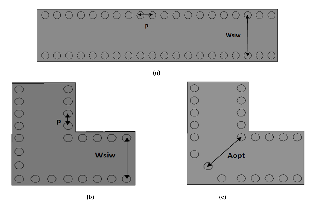 | Figure 1. Top view of SIW junction structure in H-plane (a) rectangular waveguide (b) Right bend (c) Chamfered bend with Aopt=Wsiw |
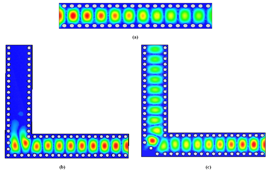 | Figure 2. Top view of TE10 electric field magnitude in H-plane SIW junction F=15GHz, (a) Rectangular waveguide (b) Right bend (c) Chamfered bend with Aopt = wsiw |
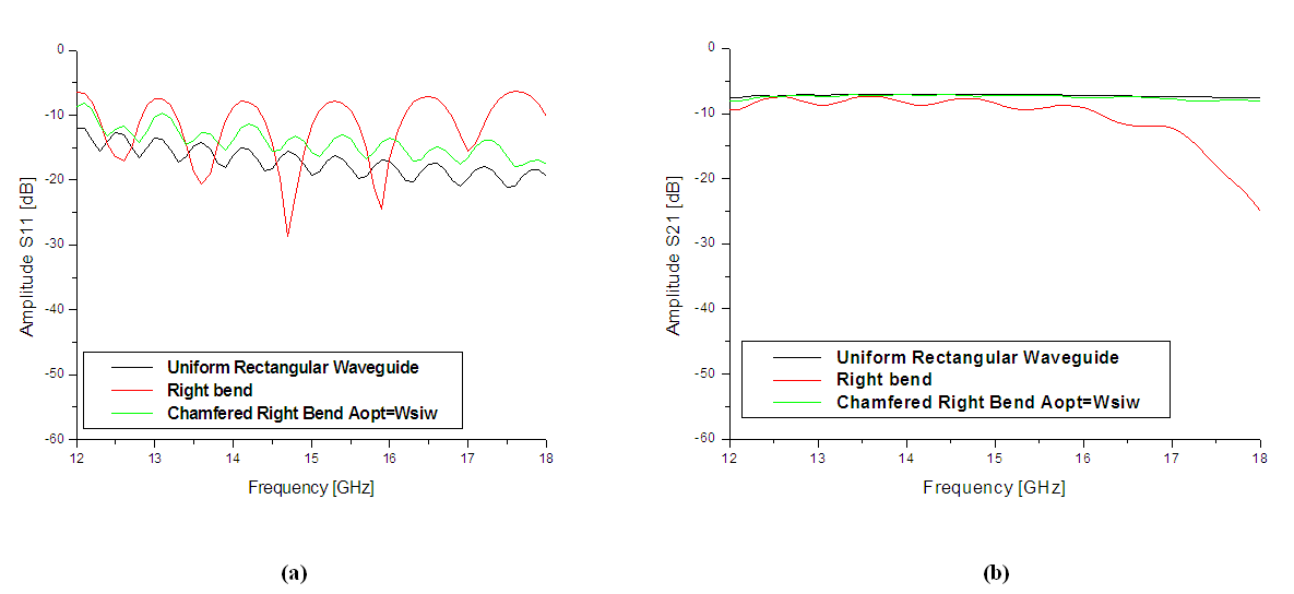 | Figure 3. (a) Reflection coefficient of H-plane SIW junction (b) The corresponding transmission coefficient |
3. SIW T-junction with Inductive Post
- The purpose of this paper is to extend optimized H plane chamfered right bend [6] in SIW technology, to the conception more general case of cascaded H-plane as power divider. In this study we developed the T-junction [5, 2] based on two chamfered right bends Figure 3 in order to broaden frequency band, knowing that the input wave is divided into two parts and output to port2 and port3 respectively. An inductive post with optimized radius ri and position Li, is added in the T-junction in order to achieve low return losses at the input port [5]. These 3 port junctions are the cells with which we will build the more sophisticated power dividers.An interesting use for a power divider is to serve as a power supply for a network antenna, moreover if the junctions used show large bands of operation, it is very likely that the final structure [5] will in turn have a considerable bandwidth. In the optimization process we have tried to identify the parameters of the junction that significantly influence its performance. The Figure 4a shows the topology of the structure as well as important dimensional parameters. Some simulation iterations were necessary to obtain a first structure meeting our optimization criteria. This optimal junction and its simulated performances are illustrated in Figures 4-5. The propagation TE10 mode Figure 4b is not affected by the chamfered bend, allowing the wave to follow the direction of bends. The distance li between the center of the inductive cylinder and the bottom of the junction as well as its radius ri influence the optimal frequency and the level of reflection.
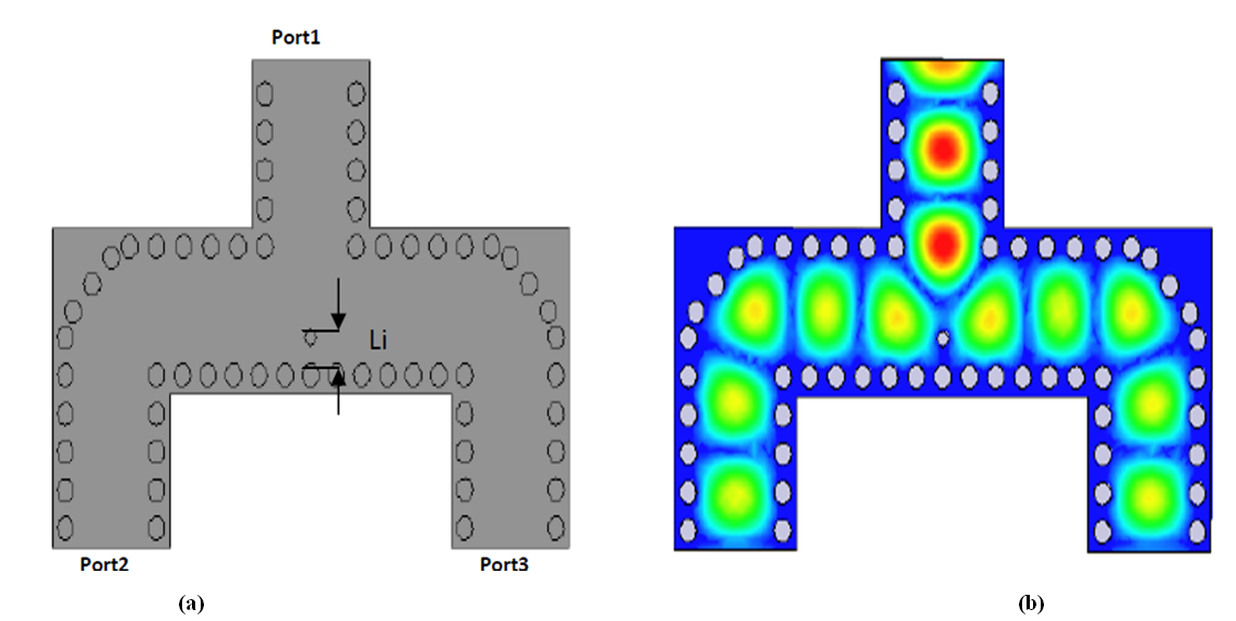 | Figure 4. (a) Top view of H-plane SIW three ports (b) TE10 electric field magnitude in SIW power divider f=15GHz |
 | Figure 5. (a) The corresponding transmission coefficient S21 and S31 (b) Reflection coefficient of SIW power divider (c) Outports phase |
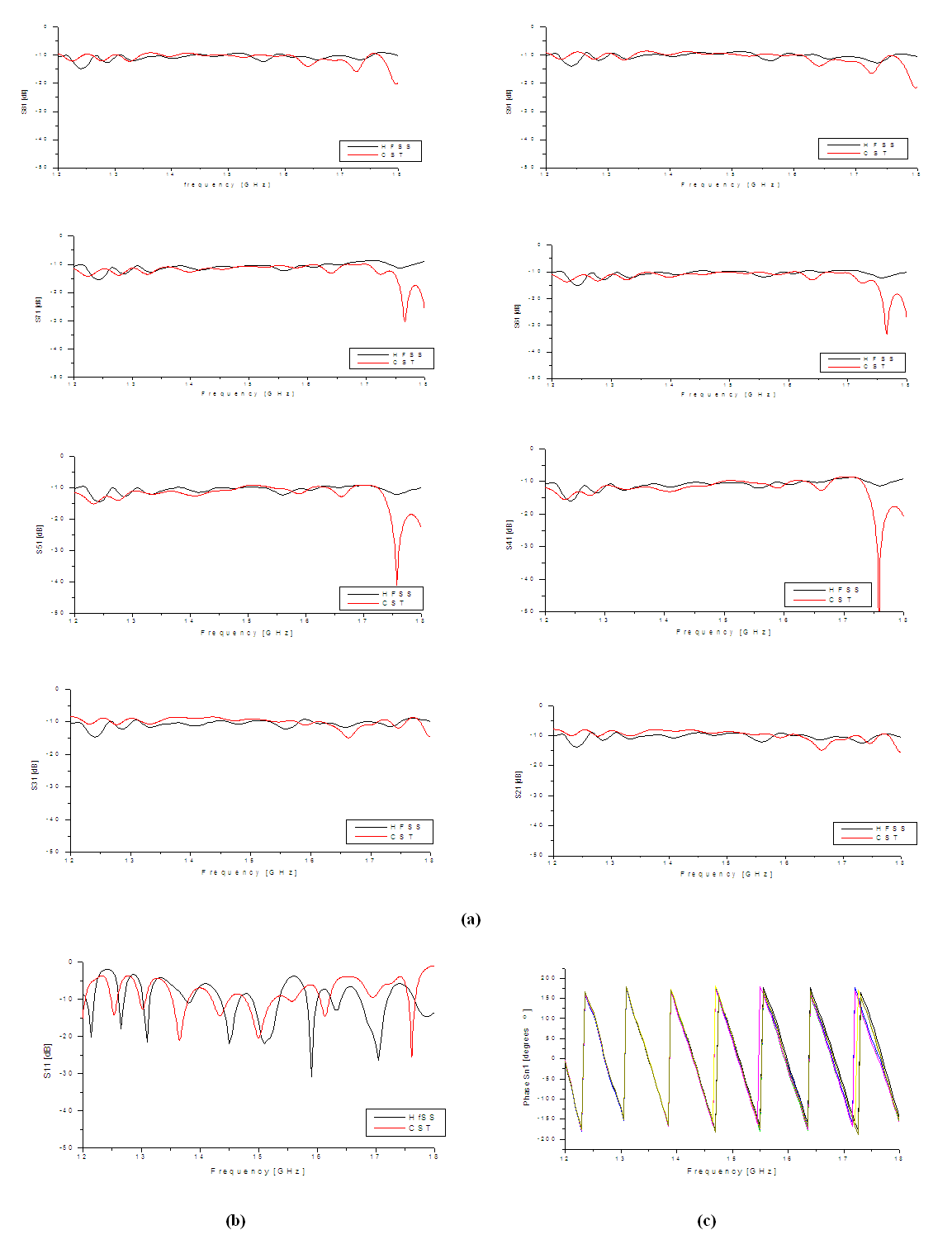
4. Validation and Simulation Results of 1x4, 1x8 and 1x16 Power Dividers
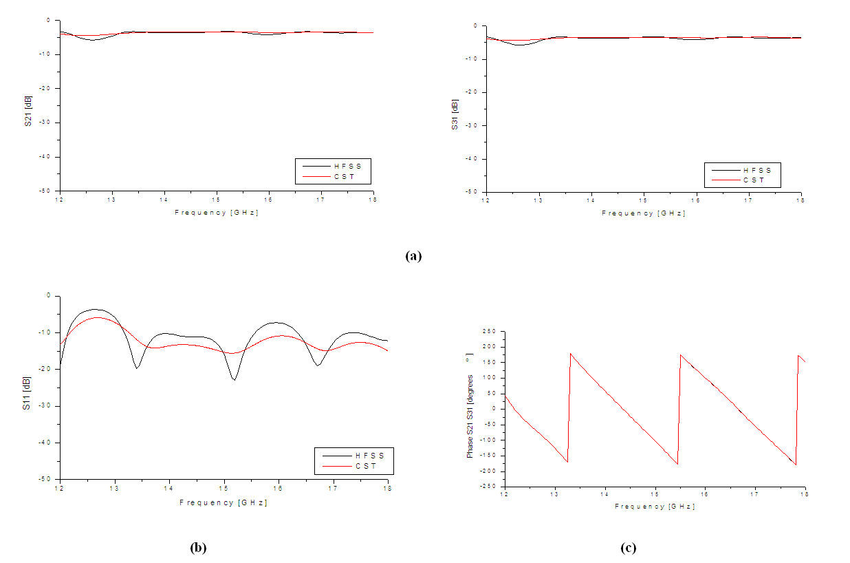
- A 1x4 power divider:The study of Ku band SIW 1x4 power divider is a logical continuation of the basic junctions. In order to join the broadband aspect and low level of reflection we opted for the previous T-junction with inductive post. These junctions allow the power to be distributed to the 4 dividers while maintaining the phase uniformity at their outputs, by minimizing the changes of direction inside the structure also to minimize the dimensions and the complexity of the circuit. We present his optimized geometry design and his simulation Figures 6-7. The suggested SIW [11-13] structure Figure 6a is designed to support TE10 fundamental mode in the operating frequency range [12-18GHz] Figure 6b. The return loss, transmission coefficients and phase of 1×4 SIW power divider simulated using HFSS and CST Microwave Studio are presented in Figure 7a-c.
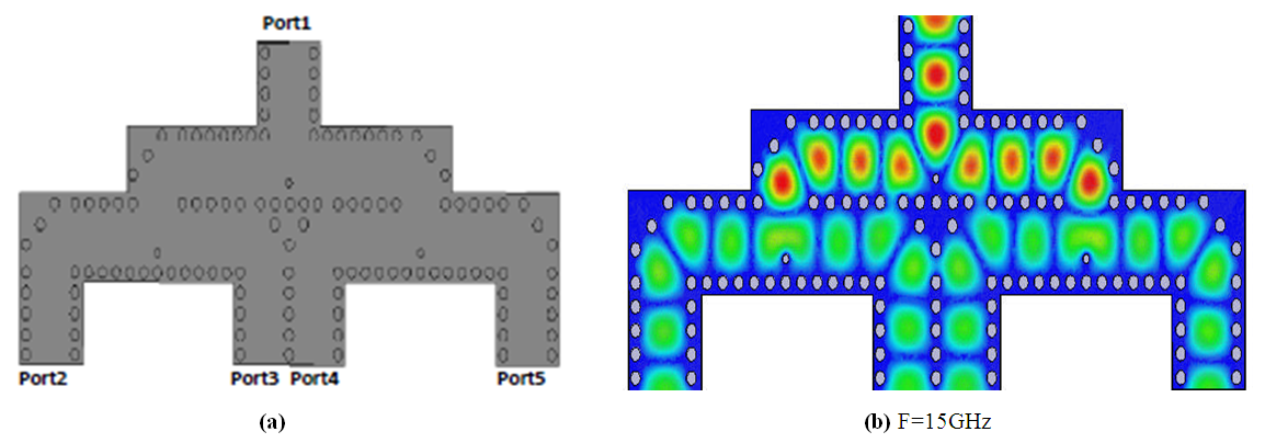 | Figure 6. (a) Top view of SIW 1x4 power divider (b) TE10 electric field magnitude in SIW 1x4 power divider |
 | Figure 7. (a) The corresponding transmission coefficient (b) Reflection coefficient of SIW 1x4 power divider (c) Outports phase |
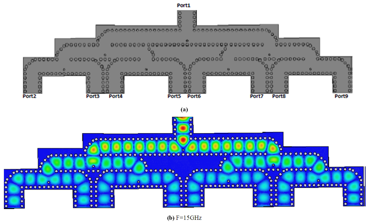 | Figure 8. (a) Top view of SIW 1x8 power divider (b) TE10 electric field magnitude in SIW 1x8 power divider |
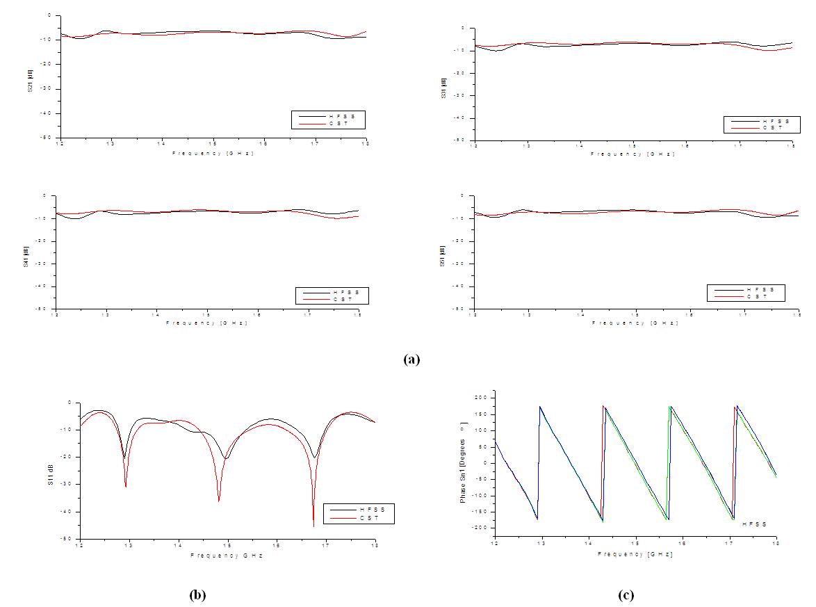
 | Figure 9. (a) The corresponding transmission coefficients (b) Reflection coefficients of SIW 1x8 power divider (c) Outports phase |
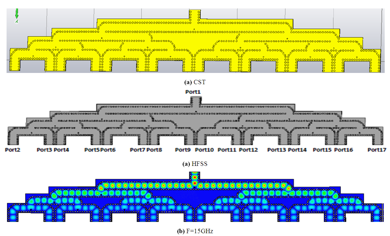 | Figure 10. (a) Top view of SIW 1x16 power divider (b) TE10 electric field magnitude in SIW 1x16 power divider |
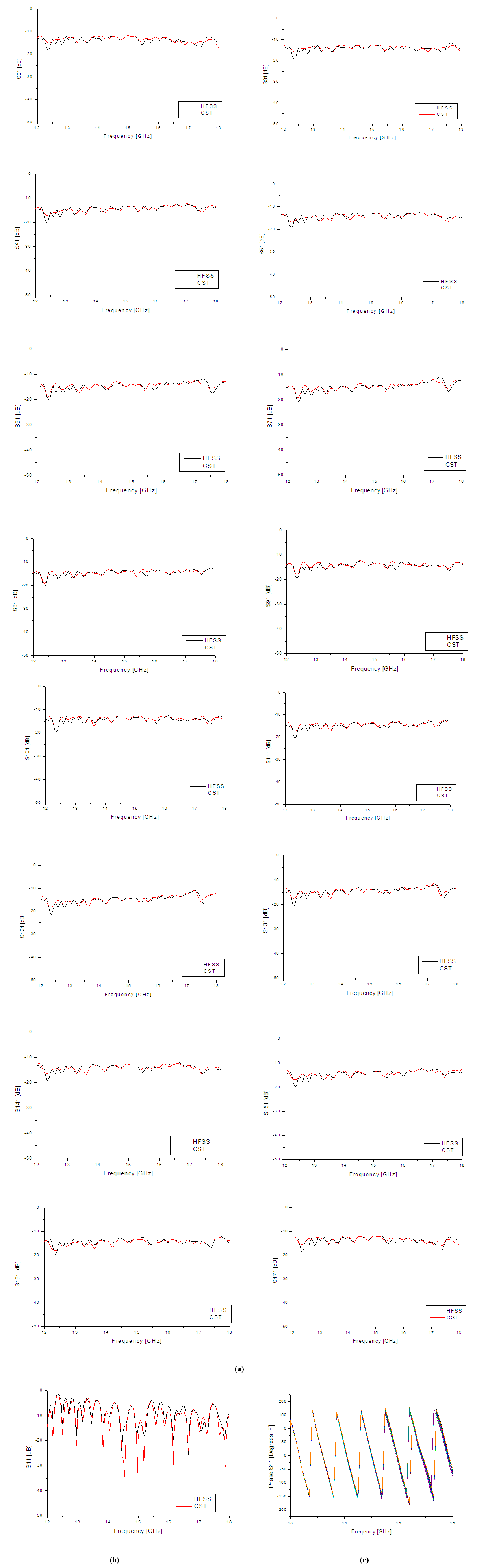 | Figure 11. (a) The corresponding transmission coefficient (b) Reflection coefficients of SIW 1x16 power divider (c) Outports phase |
5. Conclusions
- In this paper we have presented a method to design a broadband power divider in SIW technology. We approached the chamfered right bend, the T junction with inductive cylinder, the 1x4 compact divider, the 1x8 power divider and the 1x16 power divider for microwave and millimeter-wave applications. For each power divider we presented the design structure, its optimization parameters followed by simulation using 3D simulator HFSS and CST Microwave Studio. The proposed technique presents a competitive candidate for the development of millimeter wave circuits and systems. The simulated results using HFSS presents a smooth of the CST Microwave Studio results.