-
Paper Information
- Paper Submission
-
Journal Information
- About This Journal
- Editorial Board
- Current Issue
- Archive
- Author Guidelines
- Contact Us
Electrical and Electronic Engineering
p-ISSN: 2162-9455 e-ISSN: 2162-8459
2018; 8(2): 29-36
doi:10.5923/j.eee.20180802.01

FPGA-Based Analog-to-Digital Conversion via Optimal Duty-Cycle Modulation
 Abstract
 Reference
 Full-Text PDF
 Full-text HTML
Sonfack Gisèle Béatrice1, Mbihi Jean2
1Electronics Department, Faculty of Science, University of Dschang, Dschang, Cameroon
2Laboratory of Computer Science Engineering and Automation, ENSET, University of Douala, Douala, Cameroon
Correspondence to: Mbihi Jean, Laboratory of Computer Science Engineering and Automation, ENSET, University of Douala, Douala, Cameroon.
| Email: |  |
Copyright © 2018 The Author(s). Published by Scientific & Academic Publishing.
This work is licensed under the Creative Commons Attribution International License (CC BY).
http://creativecommons.org/licenses/by/4.0/

In this paper, a FPGA-based Analog-To-Digital conversion (ADC) architecture via ODCM (optimal duty-cycle modulation), is designed and implemented using software and hardware co-simulation platforms. The software platform consists of Simulink/Xilinx-based system generator blocks in which the ODCM-ADC is implemented, and of Xilinx ISE programing tool for FPGA chips. The hardware platform consists of Zynq 7000 FPGA Kit (25 MHz sampling clock), equipped with an embedded second order FPGA-based digital IIR (infinite impulse response) decimation filter, and with a PC-based JTAG communication cable/connectors. The co-simulation systems, are built and successfully tested for 3 KHz modulating bandwidth. The resulting normalized characteristics are given by: SNR = 49.55 dB, SFDR = 41,19 dB and Noise Floor Range =140 dB. These performance levels obtained under virtual and hardware co-simulation conditions, show a relevant challenge of ODCM-ADC, compared to most types of oversampling ADC techniques. As a merit, the proposed FPGA-based ADC technique is a novel and relevant ADC architecture for embedded instrumentation systems.
Keywords: Analog-to-digital conversion, Optimal duty-cycle modulation, IIR decimation filter, FPGA, JTAG communication, Virtual and hardware co-simulation, Embedded instrumentation systems
Cite this paper: Sonfack Gisèle Béatrice, Mbihi Jean, FPGA-Based Analog-to-Digital Conversion via Optimal Duty-Cycle Modulation, Electrical and Electronic Engineering, Vol. 8 No. 2, 2018, pp. 29-36. doi: 10.5923/j.eee.20180802.01.
Article Outline
1. Introduction
- Most artificial and natural signals to be captured for digital processing purposes are analog quantities and consists of a finite frequency spectrum. As an implication, the ADCs (analog-to-digital converters) with a suitable sampling frequency according to Nyquis’s theorem, are widely used in modern instrumentation systems. Although the ADC concept is simple ideally, building an optimal realistic ADC device has been overtime and remains, an intricate and active problem in electronic instrumentation engineering practice. This is due mainly to the fact that each family of ADC devices is designed and implemented for a target application areas, with intrinsic technical and qualitative requirements. As an example, the oversampling ADC architectures, are suitable for instrumentations problems involving servomechanisms, temperature regulation, lighting processes and audio systems [1, 2]. The most popular candidate within this class of oversampling ADC systems is the sigma-delta ADC architecture. Surprisingly, in 2012, a novel oversampling ADC architecture founded on the DCM (duty-cycle modulation) principle, has been studied and well tested with satisfactory results in [4, 5]. However, the following technological problems were outlined: Use of a PC (personal computer) as the DSP (digital-signal-processing) core for real-time oversampling high frequency on/off modulating signals, unreliability of the PC-based clock required for the oversampling process, and implementation of the digital decimation process as a Visual Basic application program. Given these technological problems, it is worth noting that the limitations related to the DCM-ADC architecture, relies on the PC-based environment used for digital signal processing tasks. Indeed, many studies conducted in most recent papers indicate that, the DCM principle provides numerous relevant technical properties and high quality [6, 7], while numerous intricate weaknesses are hidden behind the popular sigma-delta ADC architecture, e.g., higher structural complexity, higher order n-bit decimation filter for reaching a good accuracy, lack of exact analytical models for rigorous design and analysis purposes, and more. It is worth noting also that, although the DCM principle has also been used satisfactory beyond ADC application areas, e.g., DAC (digital-to-analog converters) [8-11], signal transmission [12, 13], and power electronics [14-16], little attention has been devoted to the ODCM problem studied in [17], under Matlab/Simulink framework. The aim of this paper is to develop a FPGA-Based framework for software-hardware co-simulation processes of an ODCM-ADC architecture (virtually modelled in [17]). The co-simulation results obtained at this development research will be very relevant, for a realistic evaluation of technical requirements when using FPGA-based ODCM-ADC technology in embedded electronic instrumentation systems. The remaining content of the paper is organized in several additional sections. Section 2 deals with a brief recall on the ODCM-ADC architecture. In section 3, the FPGA-Based ODCM-in ADC co-simulation processes are presented. Then, the FPGA-Based ODCM-ADC design is conducted in section 4 from Simulink/Xilinx block sets and also using Xilinx ISE programming tool for FPGA chips. Furthermore, in Section 5, the prototyping FPGA-based ODCM-ADC converter is well tested from software and hardware co-simulation processes, and a sample of relevant results obtained are presented. Finally, the paper is concluded in Section 6.
2. Recall of ODCM-ADC Architecture
- A similar schematic diagram of an ODCM-ADC designed in [1], is recalled in Fig. 1. It consists of two main parts, connected in tandem, i.e., an upstream optimal DCM circuit (see Fig. 1(a)) with modulating input x and DCM output xm(t), and a downstream optimal digital IIR (Infinite Impulse Response) filter (see in Fig. 1(b)). The optimal DCM circuit is designed according to a set of nonlinear parametric optimization problems with constraints, whereas the optimal IIR filter is synthesized according to the weighted least pth norm specifications.
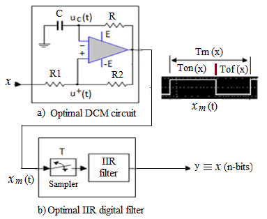 | Figure 1. ODCM-ADC architecture |
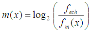
 | (1) |
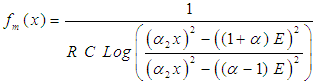
 | (2) |
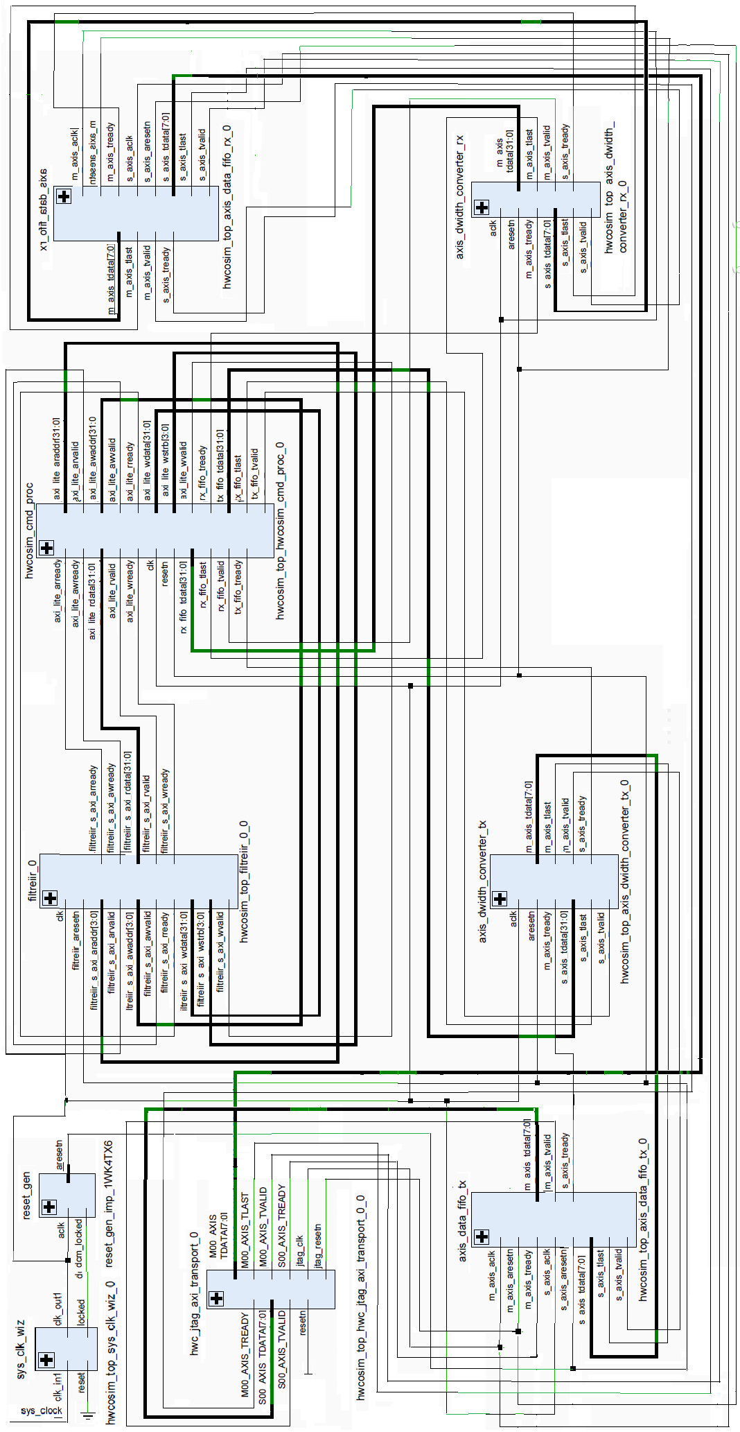
3. FPGA-Based ODCM-ADC Design
- The FPGA-Based ODCM-ADC design is conducted under Simulink workspace, according to the schematic diagram presented in Fig. 2. The upstream subsystem shown in Fig. 2(a) is a Simulink-based model of the DCM circuit given by (1), with analog modulating input Xs ≡ x as in Fig. 1(a), and with a sampled modulation output xm.
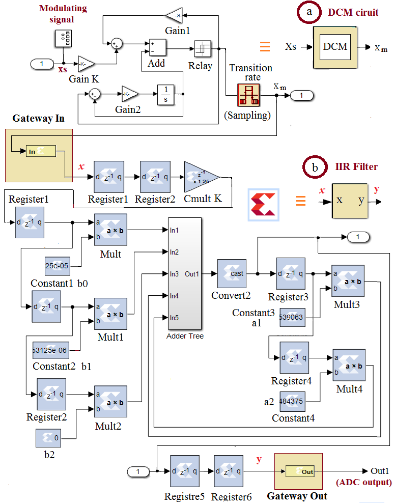 | Figure 2. FPGA-Based ODCM-ADC design architecture |
 | Figure 3. RTL diagram of the digital IIR decimation filter |
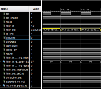 | Figure 4. Waveforms of the FPGA-Based ODCM-ADC generated under Xilinx ISE |
4. Co-Simulation of the FPGA-Based ODCM ADC
- The co-simulation is a powerful modern technique, which is widely used nowadays for rapid testing and evaluating at design time, the predicted and realistic performance of a DSP-based system [18, 19]. Indeed, the co-simulation processes require a PC-based virtual simulation application for DSP (digital signal processing), and a target DSP board equipped with an embedded version of the application code to be simultaneously executed with the virtual application. Both PC and DSP board are connected via an appropriate communication cable/connectors (USB, Ethernet or JTAG). Thus, in a hardware co-simulation context, digital signals involved in a DSP/FPGA chip, are uploaded automatically to the PC-based virtual platform for real-time monitoring.During a co-simulation session, the virtual simulator and hardware DSP are simultaneously launched and driven under the same operating conditions (input and parameters), while the real-time behavior of the hardware DSP is brought to the virtual simulation environment for the sake of rapid design, performance visualization and evaluation. The co-simulation environment created in this research work for rapid computing and evaluating both predicted and experimental characteristics of the prototyping FPGA-based ODCM-ADC, is presented in Fig. 5.
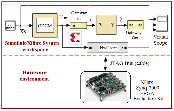 | Figure 5. Hardware Co-Simulation environment |
5. Co-Simulation Results
- A number of relevant results have been obtained when testing the characteristics of the prototyping FPGA-Based ODCM-ADC in the co-simulation framework. These relevant results are summarized in Fig. 6. Fig. 6(a) shows in the time domain the graphs of 3 signals involved (modu- lating, hwCosim output and Gateway output). It is a challenge to observe in Fig. 6(b) that, even under widely zoomed vision scale, the gap between the graphs of modulating and hwCosim output signals remains negligible. In addition, the values of SNR, SFDR and NOISE FLOOR range computed from Fig. 6(c) and Fig.(d) are 49.55 dB, 41.19 dB and 140 dB respectively.
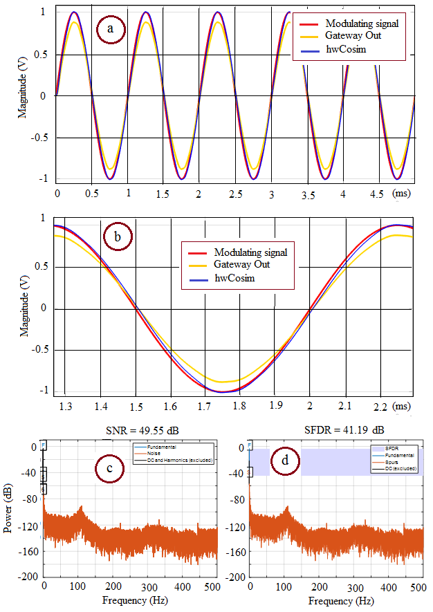 | Figure 6. Summary of a sample of Co-simulation results obtained |
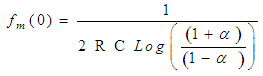
 | (3) |
 | (4) |
 | (5) |
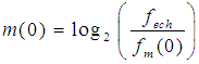 | (6) |
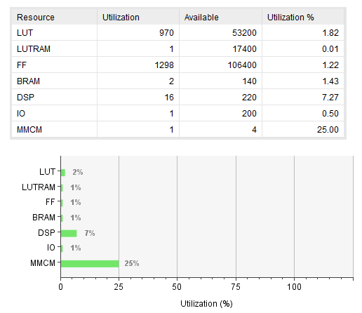 | Figure 7. Proportion of FPGA resources used for the implementation of ODCM-ADC/ |
6. Conclusions
- This paper presents the design and FPGA-based implementation, as well as the hardware co-simulation of the proposed ODCM-Based ADC. The design and co-simulation have been sussesfuly implemented on a target Xilinx ZYNQ 7000 FPGA memory kit. It is worth noting that the ODCM-based ADC owes its low implementation cost and high quality (stability, accuracy and robustness) to both the harware simplicity and the topological relevance (negative and positive feedback loop) of its interfacing DCM circuit. As a relevant mayor finding, the new FPGA-based ODCM-ADC presented in this paper, might be used as a new potential architectural solution for embedded instrumentation systems.