Electrical and Electronic Engineering

p-ISSN: 2162-9455    e-ISSN: 2162-8459

2017;  7(3): 85-89

doi:10.5923/j.eee.20170703.03


An Optimized Performance Amplifier

Amir Ashtari Gargari, Neginsadat Tabatabaei, Ghazal Mirzaei

School of Electrical and Computer Engineering, University of Tehran, Tehran, Iran

Correspondence to: Amir Ashtari Gargari, School of Electrical and Computer Engineering, University of Tehran, Tehran, Iran.

Email:

Copyright © 2017 Scientific & Academic Publishing. All Rights Reserved.

This work is licensed under the Creative Commons Attribution International License (CC BY).
http://creativecommons.org/licenses/by/4.0/

Abstract

Amplifiers are the key components in analog or mixed-signal systems due to their domination on the system power, area, and performance parameters. Their design however, tends to become more challenging as the technology scaling continues. This work proposes an automatic design of amplifiers utilizing the induced benefits of the evolutionary algorithms. The proposed scheme is analyzed and designed on a two-stage amplifier in a 65nm process to attain the benefits of advanced CMOS technologies. An optimization technique using computational intelligence is applied to improggve the design process and the overall circuit performance. The proposed amplifier illustrates significant improvements in terms of performance, power, and area efficiency as compared with the conventional analog circuit designs.

Keywords: Computational intelligence, Automatic design, Optimization algorithm, Analog circuit design, Operational amplifier

Cite this paper: Amir Ashtari Gargari, Neginsadat Tabatabaei, Ghazal Mirzaei, An Optimized Performance Amplifier, Electrical and Electronic Engineering, Vol. 7 No. 3, 2017, pp. 85-89. doi: 10.5923/j.eee.20170703.03.

1. Introduction

Ever growing CMOS technology scaling makes amplifier design more complicated and a key limiting factor in mixed-signal power/performance enhancement. Optimization algorithms can be a promising solution that overcomes the technical barriers in high-performance amplifier design by utilizing their capabilities of chip area, design time, and complexity reduction [1-4].
Recently, some automatic circuit designs have been proposed [5, 6]. In a conventional amplifier design method, one of the major challenges is considering the desired silicon area, power/performance efficiency, and noise sensitivity as it is the most important block in the system. However, utilizing an efficient optimization approach for design of analog circuits has not been investigated yet. Moreover, the key specifications of the amplifier design such as noise sensitivity and operation bandwidth are not considered simultaneously in the previous works [7-9].
In this work, a novel performance improvement approach is proposed that minimizes the computational effort while keeping the desired performance accuracy, simultaneously. This method uses a simulation-based multi-objective evolutionary algorithm to obtain the optimal circuit design points inside a limited practical deign space [10-12]. Focusing on a limited practical deign space results in reduced simulation time and computational burden whilst keeping a desired level of accuracy.
The rest of the paper is organized as follows. Section 2 discusses the proposed amplifier design approach and the implemented circuit structure. Section 3 shows the simulation and evaluated results. Finally, a conclusion is given in Section 4.

2. Proposed Algorithm

The proposed optimization algorithm and the related MATLAB-HSPICE connection are shown in Fig. 1. The start point of this approach is to define the amplifier topology, process variation models, and the related performance functions [13-15]. The algorithm also generates a testbench netlist for the defined circuit topology and derives a set of design parameters under specified max/min conditions to change the amplifier performance. Then, the design space will be explored until obtaining the desired performance and finding out the best design point concerning a multi-objective function.
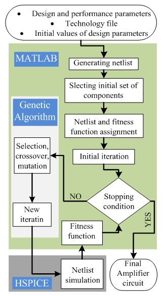
Figure 1. Optimization process
Since the circuit performance is defined as a function of design parameters, the amplifier design target is to explore the design space and obtain a set of candidates that satisfy all the fitness functions and their corresponding constraints.
In an amplifier design problem, different performance parameters such as DC gain, power consumption, unity gain bandwidth (UGBW), and phase margin conflict one another.
Therefore, we face a multiple-objective problem. Also, it is impossible to find a specific design solution that gives the optimum value for any performance parameter. Thus, the optimization solver tries to find a set of non-dominated solutions which are the performance trade-offs and are named Pareto-optimal. Once a set of Pareto-optimal points on the design space is found, the candidate circuits with desired performance are evaluated about the best overall performance. Other solutions which do not satisfy the required specifications are removed from the process.
Among the optimization search engines, evolutionary algorithms are able to obtain the Pareto-front, over only one automatic design process. In the evolutionary-based algorithms, problems with more than one fitness function (i.e., multiple-objective problems) are generally specified as (1).
(1)
where ym(x) is an N fitness functions set and ci(x) is an I constraint set. Multiple-objective evolution corresponds the feasible solutions in the design space to an objective space which has the number of dimensions equal to the objective number.
Since the key design objective is minimizing the power consumption while meeting all other performance requirements, the applied technique combines most of important performance parameters except power consumption into a single objective. The objective function is a kind of weighted summation as shown in (2)
(2)
Having decision variable vector 
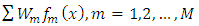
with n dimensions in the design space, X, (i.e., X introduces the whole design space), the amplifier optimization problem can be formulated in a way to find a vector, x*, that can minimize a set of K objective functions . The design space, X, is commonly constrained by a set of equality restrictions represented by
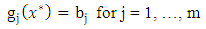
(2)
A. The simulated circuit architecture
This work tries to automatically design a fully differential operational transconductance amplifier (OTA) which can be used in the first stage of an 8-bit pipelined analog to digital converter (ADC). The implemented amplifier structure is a fully-differential folded-cascode OTA shown in Fig. 2(a). Also, Fig. 2(b) and (c) show the bias circuits of the amplifier. The common-mode feedback circuit is depicted in Fig. 2(d). As it is shown in fig. 2, this structure presents several optimization variables including the differential transistor sizing (i.e. M1 and M2), the active load, and the current source transistor sizing (i. e. M3-M10). The multi-objective optimization process has been implemented in a way to satisfy the most key performance functions of the OTA as following:
Sampling frequency >200 MHz
Input frequency>98.4375 MHz sin wave
Open-loop DC gain, AOL(0)>AOLmin,
Output voltage swing> Voutpp_min
Phase margin, PMmax>PM>PMmin
Power, PWmax>PW
Common mode range, CMMR>CMRRmin
unity gain bandwidth, UGBW>, UGBWmin
Slew Rate, SR>SRmin
Transistors aspect ratio, W/Lmax>W/L>W/Lmin
While the design variables are transistors width, W, aspect ratio, W/L, and the bias currents.
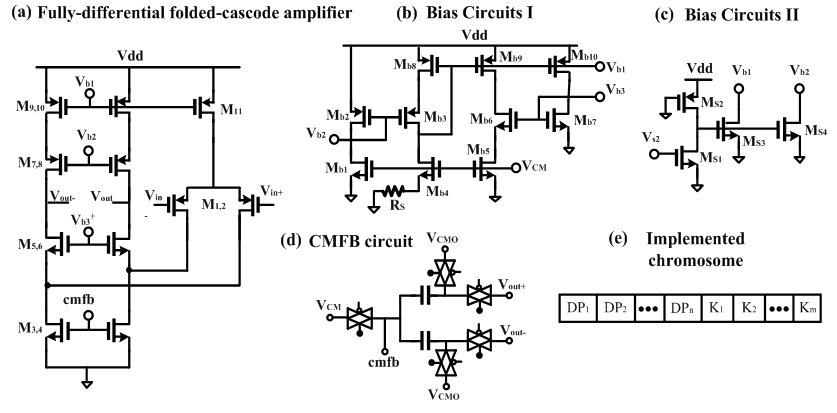
Figure 2. Implemented amplifier architecture and corresponding chromosome
B. Multi-objective optimization
Now that all performance and design parameters are specified, a genetic algorithm (GA) chromosome can be defined as a string of design parameters. The implemented OTA corresponding chromosome has been shown in Fig. 2 (e) and the GA initial population can be generated based on this structure. To optimize the computational efficiency, the population (i.e., number of candidates in each iteration) is selected 40. Now the remaining evolutionary parameters such as mutation, selection, and crossover should be selected. To select each generation parents, the standard biased stochastic uniform technique [16, 17] was implemented. In this selection, GA lays out a line that corresponds each parent to a line length section which is proportional to the parent scaled value. Also, between several devised forms of crossover, the utilized method in the work is the two-point type. This type of crossover generates two random integers between 1 and number of variables and each gene of the final vector is selected from the first or second parent if the corresponding vector is less than the first point, between two points, or more than the second point. Then, the selected genes define the next generation population. The last action on the generated population is mutation which can be described as the occasional random alteration of genes inside each chromosome. The utilized type of mutation method in this work is uniform. This type of mutation creates a random number between 0 and 1, and if it is smaller than the current mutation probability, the gene value can be randomly changed to a new value according to the generated mutation. Herein, the mutation probability value is fixed to 0.06. The stop condition for the evolutionary algorithm is a fitness limit which stops the optimization process when obtaining a desired overall fitness value. When the GA stopes, the best chromosome is converted to the amplifier testbench netlist which will be simulated in HSPICE for performance extraction and then it will be analyzed to evaluate the fitness functions.
The defined fitness functions are the weight summations of the performance parameters. The same netlist is applied to define both phase margin and open loop DC gain for each candidate. Power dissipation is also estimated by multiply the voltage supply with the average of supply current. The silicon area is estimated by summation of the capacitors and transistor active areas. A total of 20 generations each with a population size of 40 are used in this work, creating the total number of optimization candidates as 800. During each evolutionary iteration, the GA tries to improve the design parameters and change their weight vectors to attain a greater fitness result, and thus enhances the performance functions. The optimization result is a full set of design parameters, performance functions, and their corresponding weight vectors.

3. Simulation Results

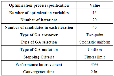
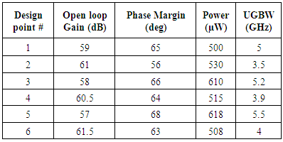
Simulated in a 65nm CMOS technology with a power supply voltage of 1.0 V, the design performance has been verified at different process corner cases including slow, nominal, and fast models for both nMOS and pMOS devices as well as temperature variations spanning from –40°C to 85°C. Also, the actual MOS devices have been implemented to realize the switches controlled by different clock phases. To damp the oscillations caused by the bondwire parasitic inductors, the MOS decoupling capacitors are implemented. The optimization process is depicted in Fig. 2. Table 2 also lists an overal specification of the optimization process.
Table 1. The evolutionary specifications of the proposed algorithm
     
A summary of the performance parameters for the Pareto-front points are listed in Table 2. After a total number of 2,000 simulations running through the evolutionary process and attaining 76 Pareto-front points, only 8 of them were located inside the feasible region. Fig. 3 shows these points.
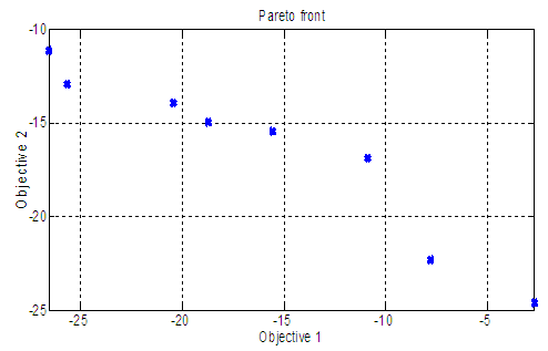
Figure 3. Obtained pareto front points
Table 2. The Pareto-front points performance values
     
By focusing only on this region over the performance optimization, the computational burden was reduced about 40 percent and the total design time was about 2 hours on a high-performance computing PC with 64GB RAM 8-core Intel CPU.
To evaluate the optimization results, Fig. 4 (a) and (b) show the open loop gain and phase margin plots before and after the multi-objective optimization, respectively.
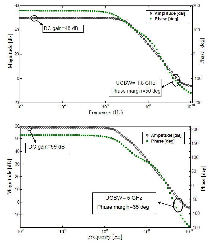
Figure 4. Frequency response (a) before and (b) after optimization
This paper presented a new amplifier circuit optimization approach that achieves an overall performance improvement through a multi-objective evolutionary algorithm and finds a set of optimal performance points on the Pareto-front. The evolutionary process based on a genetic algorithm is implemented to search the design space and find the best solutions in the feasible region. The approach can be general enough to be implemented on any analog circuit topology and result in minimized computational burden due to only concentrating on a restricted feasible design region.

References

[1]  J. Park, J., et al., “Parasitic-aware design and optimization of a fully integrated CMOS wideband amplifier,” In Proceedings of the 2003 Asia and South Pacific Design Automation Conference, pp. 904-907, 2003.
[2]  M. Akbari, and O. Hashemipour, “A super class-AB adaptive biasing amplifier in 65-nm CMOS technology,” International Journal of Electronics Letters, pp. 1-13, 2017.
[3]  N. Mirzaie, et al., “Automatic design and yield enhancement of data converters,” Journal of Circuits, Systems and Computers, vol. 26, no. 01 pp. 29-41, 2017.
[4]  S. Jung, et al., “Variability-aware, discrete optimization for analog circuits,” IEEE Transactions on Computer-Aided Design of Integrated Circuits and Systems, vol. 33, no. 8, pp. 1117-1130, 2014.
[5]  J. Barkate, et al., “Fast, simultaneous optimization of power amplifier input power and load impedance for power-added efficiency and adjacent-channel power ratio using the power smith tube,” IEEE Transactions on Aerospace and Electronic Systems, vol. 52, no. 2, pp.928-937, 2016.
[6]  R. Gonzalez-Echevarria, et al., “Automated generation of the optimal performance trade-offs of integrated inductors,” IEEE Transactions on Computer-Aided Design of Integrated Circuits and Systems, vol. 33, no. 8, pp. 1269-1273, 2014.
[7]  L. G. de la Fraga, and E. Tlelo-Cuautle, et al., “Optimizing an amplifier by a many-objective algorithm based on R2 indicator,” IEEE International Symposium on Circuits and Systems (ISCAS), pp. 265-268, 2015.
[8]  J. Dobeš, et al., “Multi-objective optimization of a low-noise antenna amplifier for multi-constellation satellite-navigation receivers,” 28th IEEE International System-on-Chip Conference (SOCC), pp. 88-93, 2015.
[9]  S. Ali, et al., “Yield model characterization for analog integrated circuit using Pareto-optimal surface,” 15th IEEE International Conference on Electronics, Circuits and Systems, 2008.
[10]  N. Mirzaie, et al., “Resilient design of current steering DACs using a transistor level approach.” Analog integrated circuits and signal processing,” vol. 90, no. 1, pp. 29-41, 2017.
[11]  R. Martins, “Multi-objective optimization of analog integrated circuit placement hierarchy in absolute coordinates,” Expert Systems with Applications, vol. 42, no. 23, pp.9137-9151, 2015.
[12]  S. Jung, S., et al., “Yield-aware Pareto front extraction for discrete hierarchical optimization of analog circuits,” IEEE Transactions on Computer-Aided Design of Integrated Circuits and Systems, vol. 33, no. 10, pp.1437-1449, 2014.
[13]  N. Mirzaie, et al., “Yield-aware sizing of pipeline ADC using a multiple‐objective evolutionary algorithm,” International Journal of Circuit Theory and Applications, vol. 45, no. 6, pp. 774-763, 2017.
[14]  H. Jafari, et al., “Optimizing an LNA Circuit by Combining Multi-Objective Genetic Algorithm and HSPICE,” Life Science Journal, vol.10, no. 1, 2013.
[15]  B. Liu, et al., “Analog circuit optimization system based on hybrid evolutionary algorithms,” INTEGRATION, the VLSI journal, vol. 42, no. 2, pp. 137-148, 2009.
[16]  M. C. Bhuvaneswari, et al., “Application of Evolutionary Algorithms for Multi-Objective Optimization in VLSI and Embedded Systems,” Springer, 2014.
[17]  N. Mirzaie, et al., “Evolving More Testable Digital Combinational Circuits,” International Conference on Computer Design (CDES), pp. 40-45, 2010.