-
Paper Information
- Next Paper
- Previous Paper
- Paper Submission
-
Journal Information
- About This Journal
- Editorial Board
- Current Issue
- Archive
- Author Guidelines
- Contact Us
Electrical and Electronic Engineering
p-ISSN: 2162-9455 e-ISSN: 2162-8459
2017; 7(2): 43-47
doi:10.5923/j.eee.20170702.06

High Efficient AC/DC Converter
 Abstract
 Reference
 Full-Text PDF
 Full-text HTML
Mayuri R.1, K. Purushotham2, Bharathi Rao1
1Dept. of E & E, St. Joseph Engineering College, Vamanjoor, Mangaluru, India
2Dept. of E & E, Malnad College of Engineering, Hassan, India
Correspondence to: Mayuri R., Dept. of E & E, St. Joseph Engineering College, Vamanjoor, Mangaluru, India.
| Email: |  |
Copyright © 2017 Scientific & Academic Publishing. All Rights Reserved.
This work is licensed under the Creative Commons Attribution International License (CC BY).
http://creativecommons.org/licenses/by/4.0/

There is a continuous increased use of power electronic drive systems in the process industries such as paper mills. The topology of the power converters is being continuously evolved to improve the performance of the drive system. This work addresses such advancement in the power converter system used in the drive system. This project work proposes a single-stage High-Power-Factor AC/DC Converter that is derived from the integration of a Buck-Boost Converter and a Flyback Converter. Both converters share the same active switch. It results in reduction of component count, leading to low product cost. The Buck-Boost Converter serves as a Power-Factor Corrector (PFC) that is designed to operate at discontinuous-current mode to waveshape the input current to be sinusoidal and in phase with the input line voltage. A high power factor and high efficiency can be achieved. The Flyback Converter plays the role of the DC/DC Converter that provides an isolated output voltage with very low voltage ripple. The proposed circuit is with simple control. Besides, it can meet the design goals of high power factor, low voltage ripple and low product cost.
Keywords: Flyback Converter, Buck-Boost Converter, Single-stage High-Power-Factor AC/DC Converter
Cite this paper: Mayuri R., K. Purushotham, Bharathi Rao, High Efficient AC/DC Converter, Electrical and Electronic Engineering, Vol. 7 No. 2, 2017, pp. 43-47. doi: 10.5923/j.eee.20170702.06.
Article Outline
1. Introduction
- Due to the continuous advancements in Power electronics technology, the AC/DC Converters are widely used in many power apparatuses. Traditionally, an AC/DC Converter uses a bulky capacitor cascaded after a diode-bridge rectifier to obtain a smooth DC-link voltage which is further regulated by a DC/DC Converter operating at high-switching frequencies to obtain a stable DC output voltage. Such AC/DC Converter inevitably introduces highly distorted input current resulting in serious current harmonics and low power factor. With the goals of improving the power factor, an additional power conversion stage of Power-Factor-Correction (PFC) is included in the AC/DC Converter. Inspite of its good performance, such a two-stage solution presents high cost and low efficiency. Moreover, higher power losses are induced in two power-conversion processes, leading to low efficiency. The Literature survey reveals that are successfully proposed single-stage approaches by making the PFC and the DC/DC Converter to share the active switch. The component count can be effectively reduced. This Paper presents a single-stage AC/DC Converter based on the integration of a Buck-Boost-typed PFC and a Flyback Converter. It has the advantage of simple circuit topology since only one active switch and simple control circuit are required.The Buck-Boost Converter serves as a Power-Factor Corrector (PFC) that is designed to operate at discontinuous-current mode to wave shape the input current to be sinusoidal and in phase with the input-line voltage. A unity power factor can be achieved. The Flyback Converter plays the role of the DC/DC Converter that provides an isolated output voltage with very low voltage ripple. Since only one active switch is required, the proposed circuit is with simple control. Besides, it can meet the design goals of high power factor, low voltage ripple and low product cost [1].The focus of the topology is to reduce the DC bus voltage at light load without compromising with input power factor and voltage regulation. Using special configuration of DC/DC cell does reduction of DC bus voltage and DC/DC cell works on the principle of series charging and parallel discharging. The power output of this converter can go up to 200 W [2].Converters suffer from low efficiency because of high voltage and current stresses acting on switching devices and other circuit parameters. The introduction of resonant converters along with the conventional SSPFC provides a very sensible solution for the above mentioned problem. Normally two controllers are essential to perform the operation which cause increased cost and requires more processing time. This paper proposes a single PI controller to control the both variables to provide high converter efficiency and to reduce the cost and the processing time. The proposed system provides a constant efficiency in conversion process up to 50% of full load current [3].The Flyback Converter type single-stage converter and a half wave rectifier with time-multiplexing control (TMC) for power factor correction has the advantage of better magnetic core utilization and better performance for high power applications. The voltage ripple of the main output can also be reduced. With TMC the power processes can be achieved by single transformer to reduce the cost and the size of the converter. The simulation result of the proposed converter presents, high power factor with low cost and size [4].We can utilize the bridge rectifier’s output voltage of the boost converter to modulate the duty cycle of the boost switch. As a result, the injected signal is naturally synchronized with line current. In addition, to obtain nearly constant harmonic content over a wide range of load variation, a modulation index m is used to update the injected signal with a fraction of duty cycle which reflects the load changes [5].
2. Proposed Converter Topology
- Fig.1 shows the proposed single-stage single-switch ac-to-dc converter. It consists of a low-pass filter (Lm and Cm), a full-bridge rectifier (D1 – D4), a Buck-Boost Converter and a Flyback Converter. The Buck-Boost Converter that plays the role of PFC includes the inductor Lp, diodes D5 – D7 and the active switch S1. The Flyback Converter includes S1, the transformer T1, the diodes D8 –D10 and the capacitor Co. It is seen that the output voltage of the Buck-Boost Converter Vdc is used as the input voltage of the Flyback Converter. Both converters use the same switch S1 that is gated by a PWM controller.
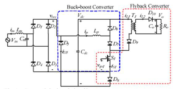 | Figure 1. Single-stage single-switch ac/dc converter |
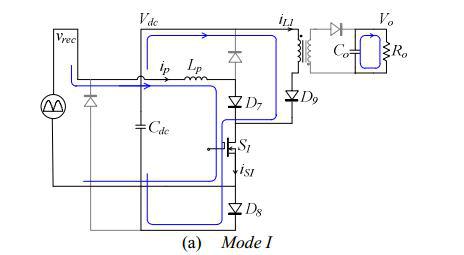 Mode II: The current ip diverts from S1 to flows through D5 and D6 to charge Cdc. The voltage across LP is equal to –Vdc, and thereby ip starts to decrease. For maintaining flux balance, the primary current of T1 is transferred to the secondary winding. At the turning-off instant of S1, iL1 is zero and iL2 is equal to N1 iL1 (t1)/N2, where N1 and N2 is the turns of the primary and secondary windings, respectively. The voltage across the secondary winding of T1 is equal to –VO and iL2 starts to decrease from a peak value. There are two possible modes following Mode II, depending on which current of ip or iL2 reaches zero first. When iL2 decreases to zero, the circuit operation enters Mode III-a. On the contrary, when ip decreases to zero, the circuit operation enters Mode III-b.
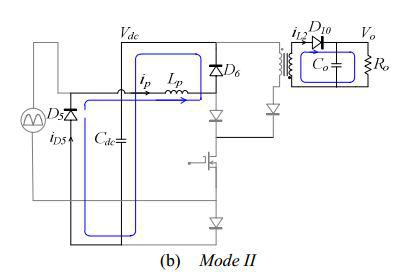 Mode III-a: S1 remains at OFF state. IL2 is zero and iP keeps flowing through D5 and D6 to charge Cdc.
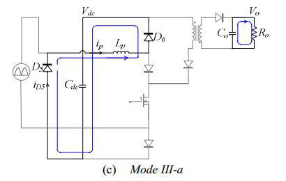 Mode III-b: S1 remains at OFF state. Ip is zero and iL2 keeps flowing through D10 to charge Co.
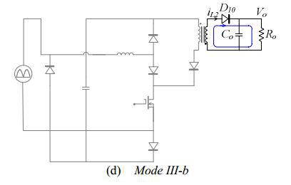 Mode IV: Both iL2 and ip are zero. Only the output capacitance Co supplies current to load Ro. This mode ends when S1 is turned ON again and the circuit operation returns to Mode I of next high-frequency cycle.
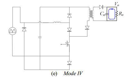
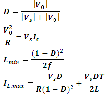
3. Design Parameters
- Buck-Boost Converter Design:
 Flyback Converter Design:
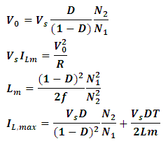
4. Simulation Results
- Fig.2 shows the simulation model of the proposed high efficient AC/DC Converter is implemented by the combination of Buck-Boost Converter and Flyback Converter. In order to obtain the required voltage rating, step down transformer is used. This rated voltage rating is given as the input to the AC/DC Converter. The obtained AC voltage is given as input to the Diode-bridge rectifier. This Diode-bridge rectifier rectifies the AC voltage to the DC voltage. The obtained DC voltage is given as input to the Buck-Boost converter. The Buck-Boost Converter is DC-DC converter which performs Buck operation or Boost operation. This DC voltage is given as input to the Flyback Converter. The Flyback Converter which is mainly used for isolation purpose and it isolates the output voltage and provides the DC voltage.
 | Figure 2. Simulation Model of AC/DC Converter |
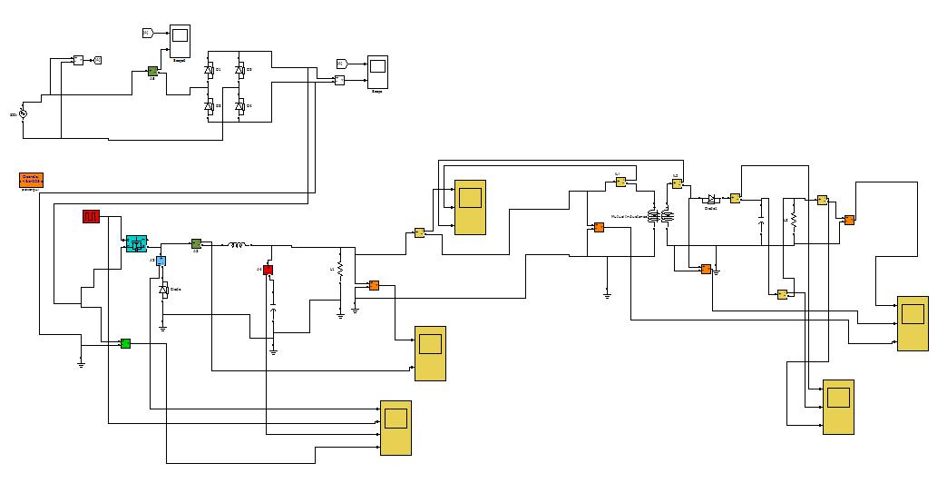
 | Figure 3. Gate pulse given to the MOSFET Switch |
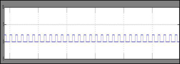
 | Figure 4. Voltage and Current measured at the input |
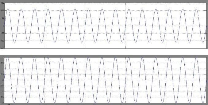
 | Figure 5. Currents measured at the output |
5. Hardware Implementation
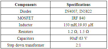
- Table 1 represents the specification of the components which is selected for the hardware module based on the designed parameter.
|
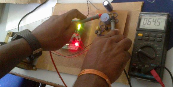 | Figure 6. Gate pulse given to the MOSFET Switch |
6. Conclusions
- AC/DC Converters are widely used in many power electronic apparatuses. The designed AC/DC Converter provides high Power Factor, using less number of components and therefore is economical compared to the traditional power electronic converters. In the industries where DC motors with less power rating are used, the Power Factor should be high which can be achieved by using the proposed converter circuit. Hence the proposed circuit acts as a power factor corrector in order to obtain high Power Factor of about 0.94 instead of very less power factor of about 0.6 or 0.7, which are used in paper mills. In paper and pulp industries, due to presence of concentrated high power non-linear loads such as electric drives, this problem is a greater concern. Different solutions exist to increase the power factor of the AC/DC Converters. In this work, high efficient AC/DC Converter has been designed by increasing power factor.