Madhavi Gatty, Chaithra Shetty, Ajithanjaya M. K.
Dept. of E & E, St. Joseph Engineering College, Vamanjoor Mangalore, India
Correspondence to: Madhavi Gatty, Dept. of E & E, St. Joseph Engineering College, Vamanjoor Mangalore, India.
| Email: |  |
Copyright © 2017 Scientific & Academic Publishing. All Rights Reserved.
This work is licensed under the Creative Commons Attribution International License (CC BY).
http://creativecommons.org/licenses/by/4.0/

Abstract
Developed multimode single leg converter replaces bidirectional and boost converter in the conventional power conversion system. There-by increasing system efficiency and fault tolerance capacity. Proposed converter has four modes of operation and these modes are simulated using MAT Lab-SIMULINK. This power electronic technology can be applied to renewable & alternative energy generation systems and electric vehicles.
Keywords:
Multimode single leg converter, Bidirectional converter, Boosts converter, Renewable & alternative energy and electric vehicles
Cite this paper: Madhavi Gatty, Chaithra Shetty, Ajithanjaya M. K., Design and Simulation of Multimode Single Leg Converter for Energy Conversion, Electrical and Electronic Engineering, Vol. 7 No. 2, 2017, pp. 33-42. doi: 10.5923/j.eee.20170702.05.
1. Introduction
Due to more consumption of energy and population rise worldwide causing environmental pollutions as well as oil price increment in recent years. Hence increase in natural gas and oil prices making people get attracted towards renewable energy sources such as solar energy, wind energy, fuel cells etc. Power electronics technology based conversion system can be applied towards “electric vehicles (EV) and renewable and alternative energy generation systems (RAEGS)”.In this energy conversion system, converters are used to boost up the generated energy from the renewable sources and this DC voltage is inverted to make it useful for home, industrial and automobile applications. Battery pack is the prime concern in power conversion system hence it is required to increase the size of the battery. As the size of the battery increased, stress on the battery as well as cost of the system increases. Hence ultra capacitors can be used to protect the battery and increase its life span.It also improves system performance and power quality of the design. Aim of the conversion system is to reduce the conversion cost with simplified system structure. Therefore multimode converter with two switches on single leg is developed to reduce the cost of the system and make the circuit structure very simple.Developed converter reduces the system cost by reducing circuit components because it operates as boost and bi-directional converter. Hence simple structure makes the diagnose of circuit easy and improves the efficiency of the conversion. The performance characteristics of the system are also improved using this converter. Control strategy and protection of the design is very important to reduce the cost. By operating two MOSFET switches on single leg, we can achieve four modes of operations. These modes are simulated using MATLAB SIMULINK with appropriate control strategy.
2. Proposed Converter Topology
Power electronics technology based conversion system can be applied towards “electric vehicles (EV) and renewable and alternative energy generation systems (RAEGS)”. This system is shown in Figure 1 which mainly comprises power generators, converter, inverter, battery/Ultra Capacitors and load. In this energy conversion system, converters are used to boost up the generated energy from the renewable sources and this DC voltage is inverted to make it useful for home, industrial and automobile applications. Battery pack is the prime concern in power conversion system hence it is required to increase the size of the battery. As the size of the battery increased, stress on the battery as well as cost of the system increases. Hence ultra capacitors can be used to protect the battery and increase its life span. It also improves system performance and power quality of the design.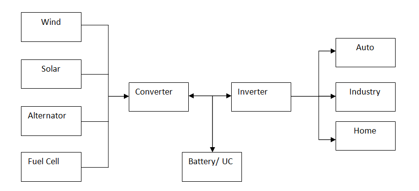 | Figure 1. Power conversion system configuration for EV and RAEGS |
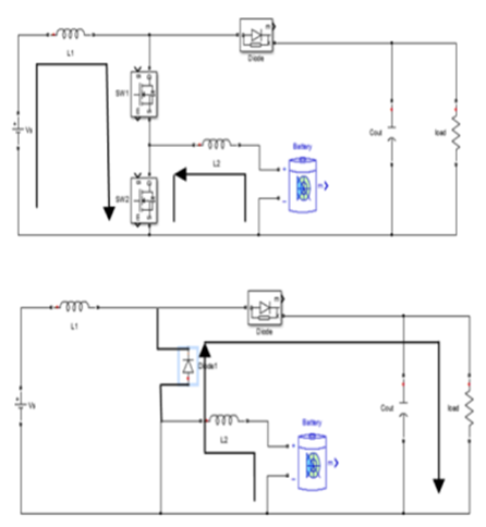
Aim of the conversion system is to reduce the conversion cost with simplified system structure. Therefore multimode converter with two switches on single leg is proposed in this project to reduce the cost of the system and make the circuit structure very simple. This is illustrated in Figure 2. It consists of two MOSFET switches, two inductors, diode and battery storage.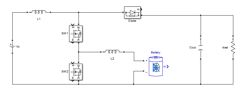 | Figure 2. Circuit of proposed multimode single leg converter |
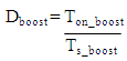
Proposed converter reduces the system cost by reducing circuit components because it operates as boost and bi-directional converter. Hence simple structure makes the diagnose of circuit easy and improves the efficiency of the conversion. The performance characteristics of the system are also improved using this converter. Control strategy and protection of the design is very important to reduce the cost. By operating two MOSFET switches on single leg, we can achieve four modes of operations. They are (1) main boost mode (mode 1), (2) boost-buck mode (mode 2), (3) boost-boost mode (mode 3) and (4) battery boost mode (mode 4). In first mode the energy generated by the source is boosted up hence it is named as main boost mode. Here no change takes place on battery power. In mode 2, input power gets boosted up along with that battery also starts charging i.e. buck. Hence it is termed as Boost-Buck mode. Whereas input power and battery charge both will be boosted during mode 3 and this mode is called Boost-boost mode. But if input is not sufficient to supply power to the load during fault conditions then mode 4 will be helpful since battery directly supplies power to the load. Therefore this mode is called Battery Boost mode. Switch control scheme for all four modes are shown in Figure 3.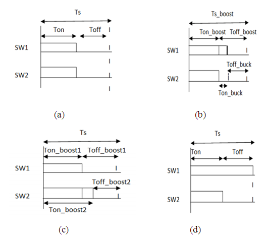 | Figure 3. Switch control scheme for (a) mode 1 (b) mode 2 (c) mode 3 and (d) mode 4 |
3. Basic Operating Principles
3.1. Main Boost Mode (Mode 1): This mode boosts source voltage to output voltage by operating two MOSFET switches. ON-OFF period for SW1 and SW2 is similar.When both the switches are closed then inductor 1 starts charging. Current flow direction during ON period is shown in Figure 4. From Figure 4(a) we can write equation for inductor 1 current as,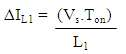 | (1) |
The inductor current during Toff can be written as | (2) |
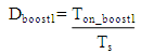
Equating above equations gives output voltage as  | (3) |
Where  | (4) |
Hence it is clear from the above equation that the voltage at output is related to duty ratio.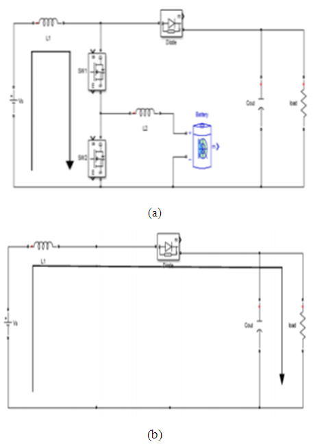 | Figure 4. Current direction during (a) ON period (b) OFF period |
3.2. Boost-Buck Mode (Mode 2): In this mode by controlling SW1 and SW2 we can achieve boost as well as buck operation. Where SW1 is ON for small duration even after SW2 turns OFF. This makes the battery to get charged up. During Ton boost, both the switches are ON making inductor L1 to charge. This operation is illustrated in Figure 5(a).During Ton boost, inductor ripple current is given by the equation, | (5) |
Stored charge in the inductor along with input is transferred to the load when SW2 turns OFF. Now inductor L1 ripple current is given by | (6) |
Equating (5) and (6) gives output voltage as | (7) |
 | (8) |
When SW2 is OFF and SW1 is ON inductor L2 starts charging. This makes the battery to get charged up during Ton buck. Current flow during Ton buck and Toffbuck is illustrated in Figure 5.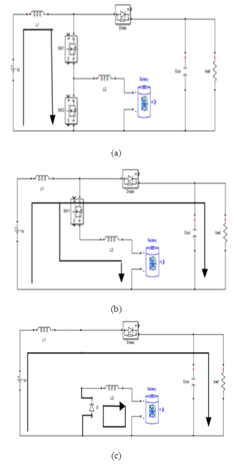 | Figure 5. Current direction during (a)Ton boost (b)Ton buck (c) Toff buck |
Inductor L2 current during Ton buck after neglecting the drops in the circuit components is given by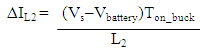 | (9) |
Inductor current decreases during buck off and boost on period 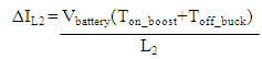 | (10) |
Output voltage for buck operation is obtained by equating (9) and (10) | (11) |
 | (12) |
3.3. Boost- Boost Mode (Mode 3): In this mode both input and battery voltage is boosted to output voltage. Where we can observe that SW2 will continue to be ON even after SW1 turns off. Current flow during this mode is given in Figure 6. | Figure 6. Current direction during (a) Ton_boost1 (b) Ton boost2 & Toff boost1 and (c) Toff boost2 |
Inductor L1 starts charging when both SW1 and SW2 turns ON during boost1 ON period. Inductor ripple current for this case is given by  | (13) |
But when SW1 turns off then SW2 will remain ON for boost OFF period which makes inductor L1 to discharge. It is expressed as 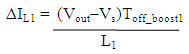 | (14) |
Equating (12) and (13) gives output voltage as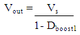 | (15) |
 | (16) |
When SW2 is ON during boost2 ON period, inductor L2 current rises and ripple current is given by the equation 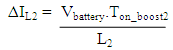 | (17) |
Inductor L2 current will be discharged when both SW1 and SW2 turns off and ripple current is expressed as 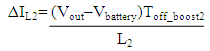 | (18) |
Output voltage for mode 3 is obtained by equating (17) and (19) | (19) |
 | (20) |
3.4. Battery Boost Mode (Mode 4): During fault conditions if source voltage is not sufficient to provide power to the output then battery boost mode is required. In this mode battery will directly supply energy to the load. This can be done by controlling SW2.When SW2 is ON during Ton period inductor L2 starts charging and current direction is shown in Figure 7. Inductor current is given by | (21) |
 | Figure 7. Current flow during ON period and OFF period respectively |
Voltage across inductor L2 along with battery voltage is transferred to the output during OFF period as illustrated in the figure. Inductor ripple current is expresses as | (22) |
Equating (21) and (22) gives output voltage as follows | (23) |
Where  | (24) |
4. Simulation Results
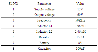
Proposed multimode single leg converter operates in four modes. To verify the system performance, these four modes are simulated using MATLAB SIMULINK based on the simulation parameters given in Table 1.Simulation model for main boost mode is shown in the Figure 8. Inductor L1 current increases during SW1 and SW2 ON period. The switches are opened then inductor current is decreased. Simulation waveform is shown in Figure 9.Simulation model and result for mode 2 is illustrated in Figure 10. Inductor L1 is controlled by SW1 and inductor 2 is controlled by SW2. Inductor L2 current is positive since battery is getting charged in this mode.Simulation model and result for mode 3 is presented in Figure 11. Inductor L2 current goes negative since battery voltage is supplied to the load with input voltage.Simulation model for mode 4 is presented in Figure 12. This mode is useful during fault condition where input is not sufficient to supply power to the load. Simulation waveform is shown in Figure 13.In this case also inductor current is negative since battery is discharged and supplying power to the load. Table 1. Simulation parameters
 |
| |
|
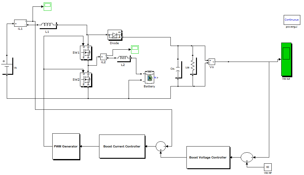 | Figure 8. Simulation model for main boost mode |
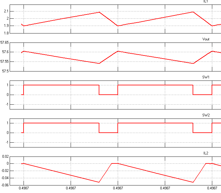 | Figure 9. Simulation result for Mode1 |
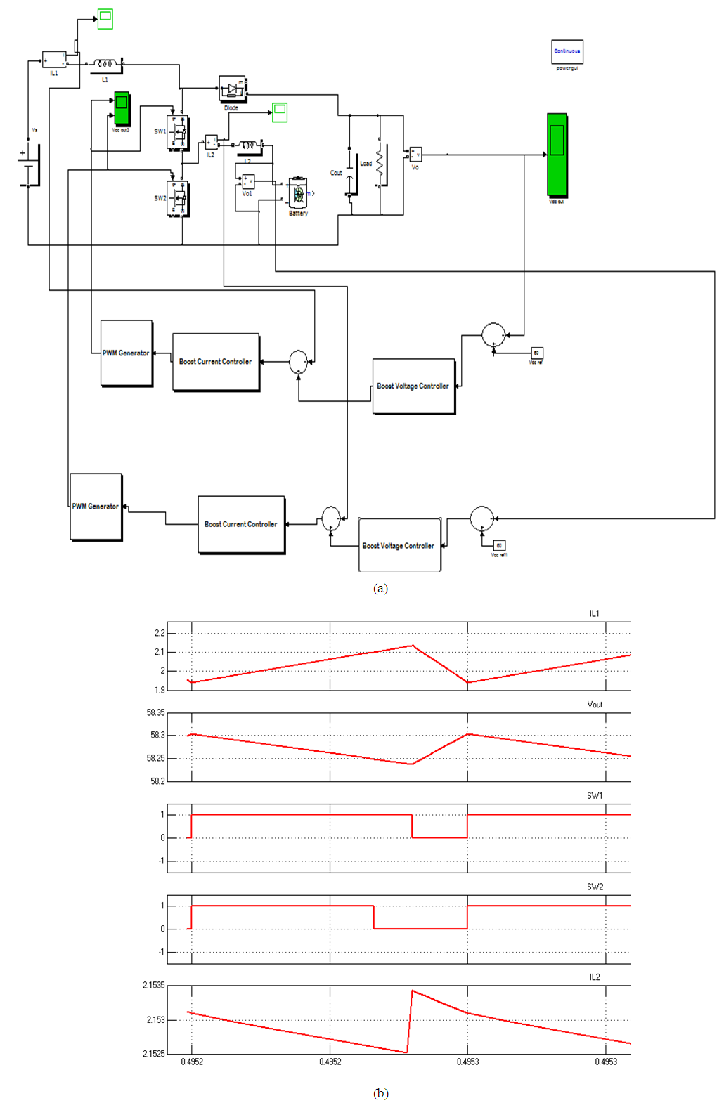 | Figure 10. (a) Simulation model and (b) Simulation result for Mode2 |
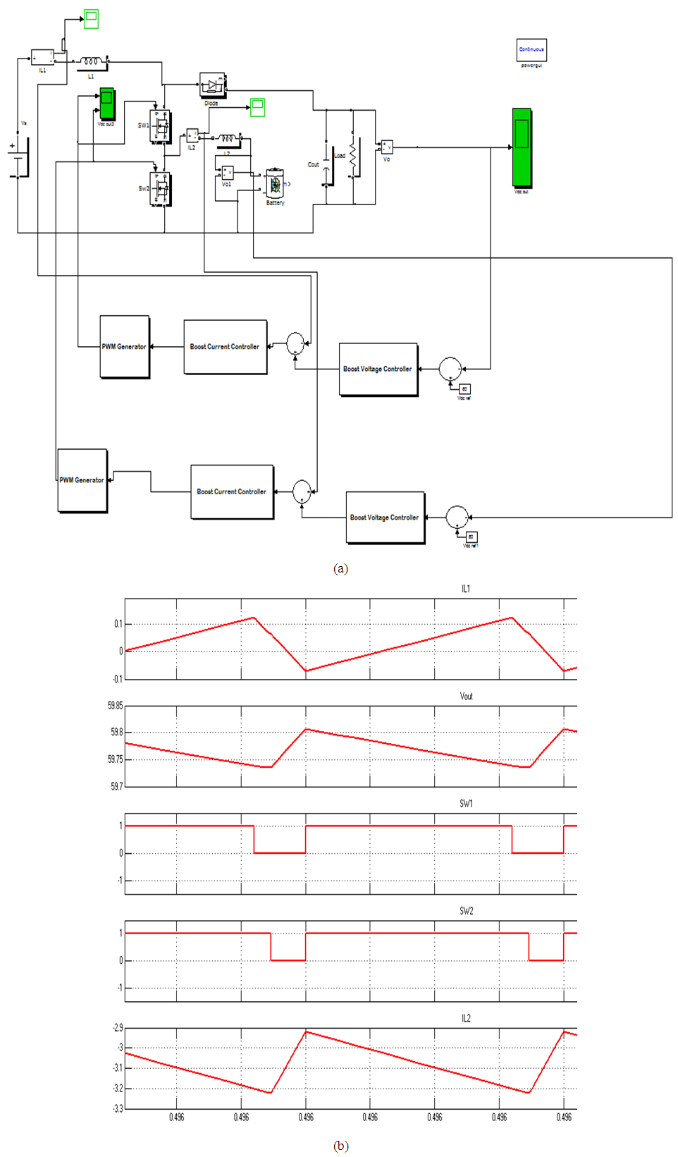 | Figure 11. (a) Simulation model and (b) Simulation result for Mode 3 |
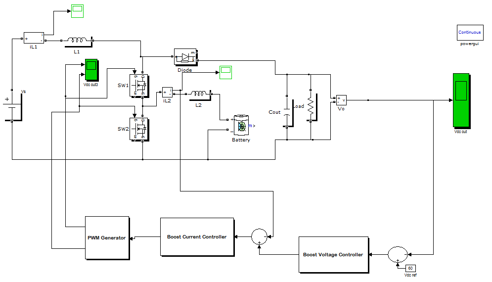 | Figure 12. Simulation model for Mode 4 |
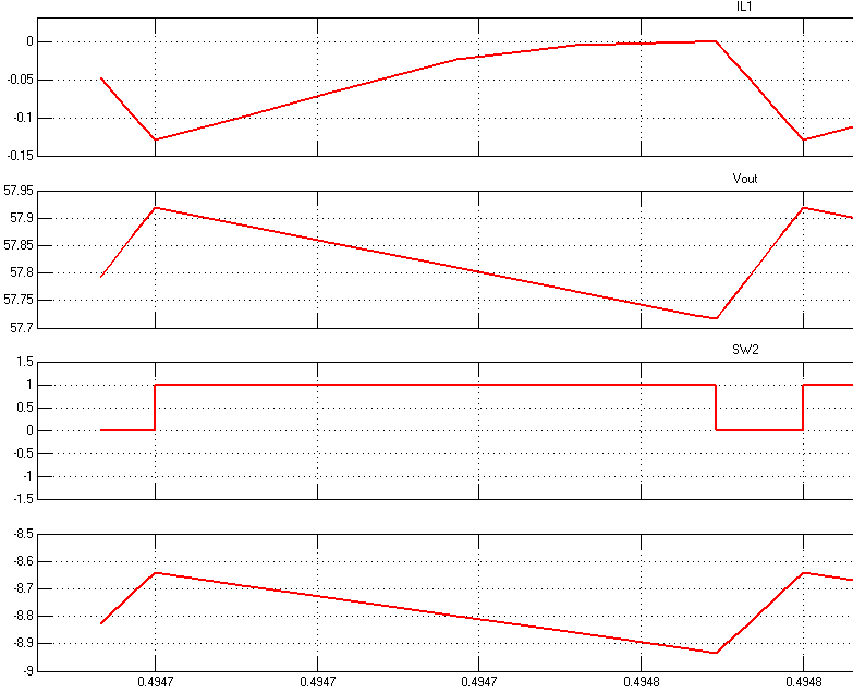 | Figure 13. Simulation result for Mode 4 |
5. Conclusions
Proposed converter operates as boost and bidirectional converter which control the power flows between source and load. There are four modes of operations. • To verify the system performance all the modes are simulated using MATLAB/SIMULINK. • System has simple structure with reduced cost. Since the numbers of components are less it is very easy to diagnose the problems.• Hence performance and fault tolerance capability of the system is also improved.• Main boost mode i.e. mode 1 is implemented experimentally using SG3524PWM circuitry which provides gate pulses for controlling the converter.• Boosted output voltage and corresponding gating signals are observed. Same method can be adopted for implementing other three modes also. This new topology can be applied to wide range of power electronic applications including energy conversion.
References
| [1] | F. Blaabjerg and Z. Chen, “Power electronics as an enabling technology for renewable energy integration,” J. Power Electron. vol. 3, no. 2, pp.81-89, 2003. |
| [2] | K. Kobayashi, H. Matsuo, and Y. Sekine, “Novel solar-cell power supply system using a multiple-input DC–DC converter,” IEEE Trans. Ind.Electron., vol. 53, no. 1, pp. 281–286, Feb. 2006. |
| [3] | R. Gopinath, K. Sangsun, H. Jae-Hong, P. N. Enjeti, M. B. Yeary, and J.W. Howze, “Development of a low cost fuel cell inverter system with DSP control,” IEEE Trans. Power Electron., vol. 19, no. 5, pp. 1256–1262, Sep. 2004. |
| [4] | C. B. Jacobina, M. B. Rossiter Correa, A. M. Nogueira Lima, and E.R. Silva, “AC motor drive systems with a reduced-switch-count converter,” IEEE Trans. Ind. Appl., vol. 39, no. 5, pp. 1333–1342, Sep. 2003. |
| [5] | Y.-J. Lee, A. Khaligh, and A. Emadi, “Advanced integrated bidirectional AC/DC and DC/DC converter for plug-in hybrid electric vehicles,” IEEE Trans. Veh. Technol., vol. 58, no. 8, pp. 3970–3980, Oct. 2009. |
| [6] | H. Li, F. Z. Peng, and J. S. Lawler, “A natural ZVS medium-power bidirectional DC–DC converter with minimum number of devices,” IEEE Trans. Ind. Appl., vol. 39, no. 2, pp. 525–535, Mar. 2003. |
| [7] | W. Liu, J. Chen, T. Liang, R. Lin, and C. Liu, “Analysis, design, and control of bidirectional cascaded configuration for a fuel cell hybrid power system,” IEEE Trans. Power Electron., vol. 25, no. 6, pp. 1565–1575, Jun. 2010. |
| [8] | P. Das, S. A. Mousavi, and G. Moschopoulos, “Analysis and design of a nonisolated bidirectional ZVS-PWM DC–DC converter with coupled inductors,” IEEE Trans. Power Electron., vol. 25, no. 10, pp. 2630–2641, Oct. 2010. |
| [9] | M. Zandi, A. Payman, J.-P. Martin, S. Pierfederici, and B. Davat, “Energy management of a fuel cell/supercapacitor/battery power source for electric vehicular applications,” IEEE Trans. Veh. Technol., vol. 60, no. 2, pp. 433– 443, Feb. 2011. |

 Abstract
 Reference
 Full-Text PDF
 Full-text HTML