Rahul V. A., Denita D’Souza, Subramanya K.
Department of E & E, St Joseph Engineering College, Mangalore, India
Correspondence to: Rahul V. A., Department of E & E, St Joseph Engineering College, Mangalore, India.
| Email: |  |
Copyright © 2017 Scientific & Academic Publishing. All Rights Reserved.
This work is licensed under the Creative Commons Attribution International License (CC BY).
http://creativecommons.org/licenses/by/4.0/

Abstract
In this paper, a novel high voltage-boosting converter is presented. This converter is constructed based on parallel and series combination of bootstrap capacitors and boost inductors during charging and discharging respectively. The proposed converter gives the output voltage 160 V DC from 24 V DC at duty cycle of 65%. The proposed converter gives a high efficiency, low output ripple and high transformation ratio by reducing the conduction losses and switching losses. Simulation of the circuit is obtained in MATLAB/Simulink.
Keywords:
Voltage-Boosting Converter, Voltage Conversion Ratio, Bootstrap Capacitors, Boost Inductors
Cite this paper: Rahul V. A., Denita D’Souza, Subramanya K., High Voltage-Boosting Converter with Improved Transfer Ratio, Electrical and Electronic Engineering, Vol. 7 No. 2, 2017, pp. 28-32. doi: 10.5923/j.eee.20170702.04.
1. Introduction
Boost converter are widely used in industry for the following applications such as discharge lamp driver, UPS, Motor drivers, and PV system [1, 2]. The boost converter or step up converters is simple in structure, but the voltage conversion ratio is less, whereas the fly-back converter possesses a high voltage conversion ratio but the corresponding leakage reactance is large. The voltage conversion ratio can be improved when the number of inductor in the circuit is increased, and these inductors are connected in series during their demagnetizing period [3, 4].Normally isolated boost converters boosts the voltage to much higher voltages with wide input ranges typically in the range of 30-60V. Since the DC-AC converter operates at high voltage and is widely used in high power applications such as in UPSs, motor drives, solar converters etc., it is required to have low voltage to high voltage DC-DC converter with high efficiency. High boosted output voltage is obtained by discharging the energy stored in the inductor and capacitor along with input voltage into the output terminals. In this paper, a brief illustration of the operation of high voltage boosting converter is given along with some simulation results provided to demonstrate the effectiveness of such converters. In [5-8], high voltage conversion ratios are achieved by coupling inductors, but the voltage spikes due to the accompanying leakage inductances and the complexity in the corresponding circuit analysis are unavoidable.
2. Proposed Converter Topology
In this paper a new high voltage boosting converter is proposed. The circuit is shown in figure 1.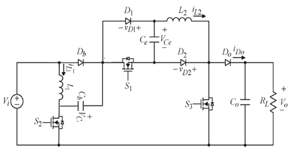 | Figure 1. Proposed High voltage boosting converter |
The converter contains three MOSFET switches S1, S2, and S3, two bootstrap capacitors Cb and Ce, three bootstrap diodes Db, D1, and D2, one output diode Do, two inductors L1 and L2, one output capacitor Co, and one load resistor RL. In addition, the input voltage is signified by Vi, the output voltage is represented by Vo.
3. Basic Operating Principles
3.1. Continuous Current Mode Operation
Figure 2 shows the illustrated necessary waveforms of vgs1, vgs2, vgs3, vL1, vL2, iL1, and iL2 for the proposed circuit operated in CCM with L1 equal to L2.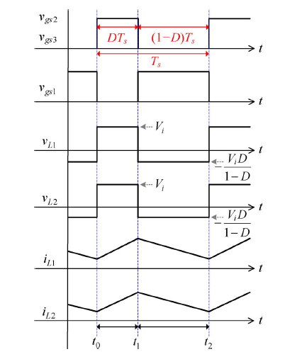 | Figure 2. Waveforms of CCM operation |
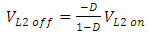
3.1.1 Mode 1 [t0 - t1]: The current flow in the proposed circuit during mode 1 in CCM is shown in figure 3. As in the figure in mode 1, S2 and S3 are turned on, but S1 is turned off. Diode Do is reverse biased, but DB, D1 and D2 are forward biased. The capacitor CB and the inductor L1 charges through switch S2. And the capacitor Ce and the inductor L2 charges through switch S3. The capacitor voltages abruptly reach to its peak value Vi. At the same time, the voltages across L1 and L2 both are Vi, thereby causing L1 and L2 to be magnetized. Also, Co releases energy to the output. 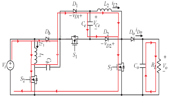 | Figure 3. Operation of the proposed circuit in mode 1 |
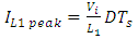
In this mode, the voltages across L1 and L2, vL1−ON and vL2−ON, can be written as | (1) |
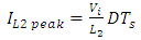
 | (2) |
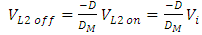
3.1.2 Mode 2 [t1- t2]: Mode 2 operation is shown in figure 4. The switches S2 and S3 are turned off, but S1 is turned on. At the same time, the input voltage plus the energy stored in Cb and Ce plus the energy stored in L1 and L2 supplies the load, thereby causing Co to be charged, Cb and Ce to be discharged, and L1 and L2 to be demagnetized. By doing so, the output voltage is boosted up, and is higher than the input voltage. According to the voltage-second balance, the voltages vL1−OFF, vL2−OFF, and Vo can be expressed as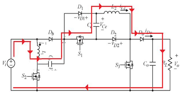 | Figure 4. Operation of the proposed circuit in mode 2 |
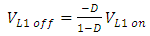 | (3) |
 | (4) |
 | (5) |
Since  , and from equation (1)-(4), Equation (5) can be written as
 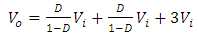 | (6) |
CCM voltage conversion ratio is then given by: | (7) |
3.2. Discontinuous Conduction Mode Operation
Figure 5 shows the illustrated key waveforms vgs1, vgs2, vgs3, vL1, vL2, iL1, and iL2 for the circuit operated in DCM with L1 equal to L2.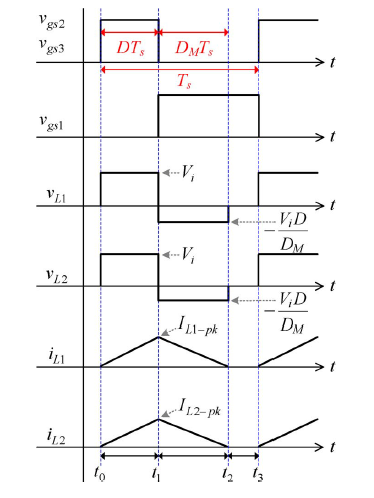 | Figure 5. Waveforms during DCM mode operation |
3.2.1 Mode 1 [t0- t1]: In this mode, the operating principle is the same as that of circuit operated in CCM in mode 1. Hence, the associated equations can be written as

 | (8) |
 | (9) |
Since L1 is equal to L2 and set to L,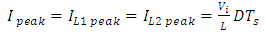 | (10) |
3.2.2 Mode 2 [t1- t2]: In this mode, the circuit operates same as CCM in mode 2. Therefore, the related equations can be written as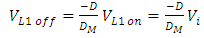 | (11) |
 | (12) |
3.2.3 Mode 3 [t2 - t3]: In this mode, all the switches and diodes are turned off, and the currents in two inductors are zero. Hence, the energy needed by the load is supplied from Co. The output voltage is expressed as | (13) |
Since 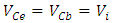 , and from equation (11) (12)
 | (14) |
Simplifying the above equation results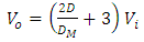 | (15) |
4. Simulation Results
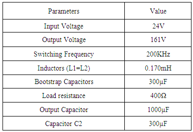
The circuit simulated in SIMULINK/MATLAB in open loop. The various parameters given according to design as explained earlier are shown in Table 1.Table 1. Simulation Parameters
 |
| |
|
The simulated circuit in MATLAB/SIMULINK is shown in Fig.6. The input DC voltage is given using DC voltage supply block. There are three switching MOSFETs in the circuit. Gating pulses are given to the switches using pulse generator. The signals so formed are given to a scope to be verified. The input voltage, output currents, current through the inductors, voltage across the output load is analyzed.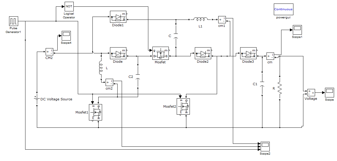 | Figure 6. MATLAB simulation of proposed topology |
4.1. Input Voltage
DC voltage of 24V is given to the converter input terminals.
4.2. Output Voltage
The output voltage obtained is as shown in Fig.7. The output voltage of 155 V is obtained and the ripple content in the output voltage is very low. The model is simulated by setting duty ratio as 0.65 to achieve this boosting.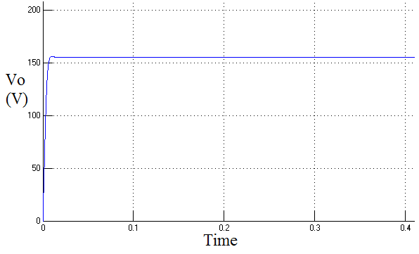 | Figure 7. Output voltage waveform |
4.3. Output Current
The output current obtained is as shown in Fig 8. The output current of 0.38A is obtained.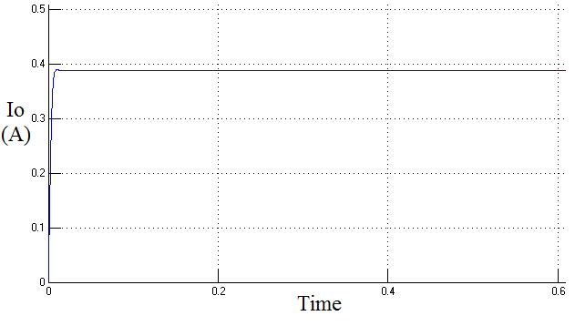 | Figure 8. Output current waveform |
4.4. Inductor Current and Gate Pulse
The inductor current and gate pulse waveform when L1=L2 is shown in Fig.9. Here the inductors are of same value. The inductor and current waveform when L1>L2 is shown in Fig.10.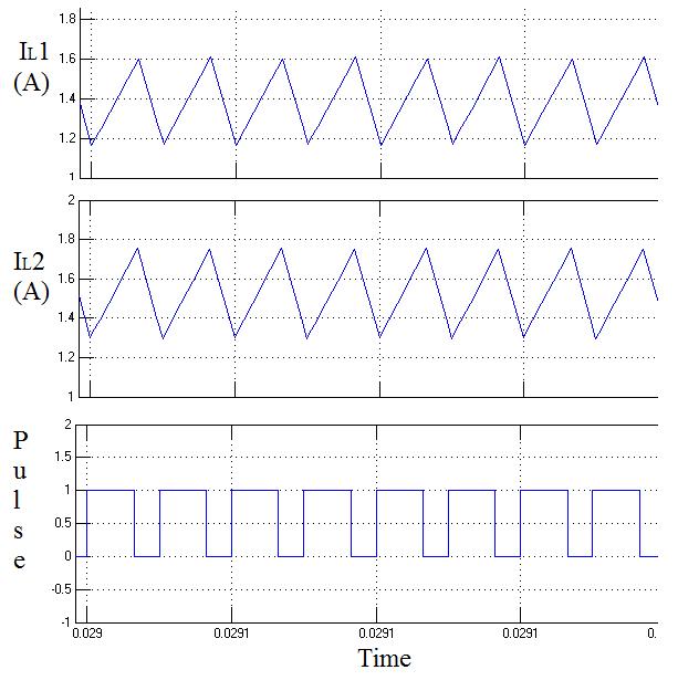 | Figure 9. Inductor current and gate pulse (L1=L2) |
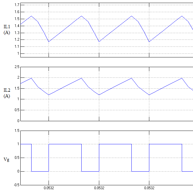 | Figure 10. Inductor current and gate pulse (L1>L2) |
5. Conclusions
A high voltage boosting converter based on inductors connected in series with bootstrap capacitors is proposed in this paper. From the experimental results, such converters exhibit good performances even with different inductances, and hence are suitable for industrial applications, such as the energy-recycling burn-in test of the buck-type converter, isolated or non-isolated. From the detailed simulations an experimental analysis, it is clear that the presented converters have the following advantages. 1. The proposed system is simple and easily constructed to achieve expected voltage conversion ratios with less loss. 2. For each converter, the power switches are easy to drive, as this converter only needs one PWM control signal to drive all three switches making its controlling simple. 3. From the simulation results, such converters exhibit good performances even with different inductances, and hence are suitable for industrial applications. 4. Proposed converters need lesser components making it less weight, low cost and compact.
References
| [1] | W. Li and X. He, “Review of no-isolated high step-up dc/dc converters in photovoltaic grid-connected applications,” IEEE Trans. Ind. Electron., vol. 58, no. 4, pp. 1239–1250, Apr. 2011. |
| [2] | H. Tao, J. L. Duarte, and M. A.M. Hendrix, “Line-interactive UPS using a fuel cell as the primary source,” IEEE Trans. Ind. Electron., vol. 55, no. 8, pp. 3012–3021, Aug. 2008. |
| [3] | D. Nicolae, C. Richards, and J. van Rensburg, “Boost converter with improved transfer ratio,” in Proc. IEEE IPEC, 2010, pp. 76–81. |
| [4] | B. Axelrod, Y. Berkovich, and A. Ioinovici, “Switched-capacitor/ switched-inductor structures for getting transformerless hybrid dc-dc PWMconverters,” IEEE Trans. Circuits Syst. I, Reg. Papers, vol. 55, no. 2, pp. 687–696, Mar. 2008. |
| [5] | K. I. Hwu and Y. T. Yau, “Voltage-boosting converter based on charge pump and coupling inductor with passive voltage clamping,” IEEE Trans. Ind. Electron., vol. 57, no. 5, pp. 1719–1727, May 2010. |
| [6] | K. C. Tseng and T. J. Liang, “Novel high-efficiency step-up converter,” Proc. Inst. Elect. Eng.—Elect. Power Appl., vol. 151, no. 2, pp. 182–190, Mar. 2004. |
| [7] | W. Li and X. He, “A family of isolated interleaved boost and buck converters with winding-cross-coupled inductors,” IEEE Trans. Power Electron., vol. 23, no. 6, pp. 3164–3173, Nov. 2008. |
| [8] | K. B. Park, H. W. Seong, H. S. Sim, G. W. Moon, and M. J. Youn, “Integrated boost-sepic converter for high step-up applications,” in Proc. IEEE PESC, 2008, pp. 944–950. |

 Abstract
 Reference
 Full-Text PDF
 Full-text HTML