-
Paper Information
- Paper Submission
-
Journal Information
- About This Journal
- Editorial Board
- Current Issue
- Archive
- Author Guidelines
- Contact Us
Electrical and Electronic Engineering
p-ISSN: 2162-9455 e-ISSN: 2162-8459
2016; 6(5): 75-79
doi:10.5923/j.eee.20160605.01

Low Power DP SRAM Design in VLSI Implementation
 Abstract
 Reference
 Full-Text PDF
 Full-text HTML
Nabihah Ahmad1, Nurdyana Mat Jainudin2
1Nano Simulation Group (NanoSIM), Department of Electronic Engineering, Faculty of Electrical and Electronic Engineering, Universiti Tun Hussein Onn Malaysia, Malaysia
2Faculty of Electrical and Electronic Engineering, Universiti Tun Hussein Onn Malaysia, Malaysia
Correspondence to: Nabihah Ahmad, Nano Simulation Group (NanoSIM), Department of Electronic Engineering, Faculty of Electrical and Electronic Engineering, Universiti Tun Hussein Onn Malaysia, Malaysia.
| Email: |  |
Copyright © 2016 Scientific & Academic Publishing. All Rights Reserved.
This work is licensed under the Creative Commons Attribution International License (CC BY).
http://creativecommons.org/licenses/by/4.0/

Static Random Access Memory (SRAM) is a major part of System on Chip (SoC) and more than half of the silicon area were filled with it. Nowadays, portable digital devices such as cell phones have a long lifespan in order for the humans to be able to rely on it and performing similar tasks as the desktop or laptop. Thus, it is important to design a low power SRAM. In this paper, a conventional Dual-Port SRAM (DP SRAM) of 2-Read/Write cell type compared with design with low power Complementary Metal Oxide Semiconductor (CMOS) techniques in terms of overall power consumption and the performances. The simulation and comparison has been designed and carried out by using Tanner Tools EDA using 0.25µm CMOS technology with 1V power supply. It shows that the Multi-threshold CMOS (MTCMOS) technique is the offer the lowest power consumption in the circuit, about 8% reduced as being compared with the conventional DP SRAM, while the Full Stack technique reduced about 6% as compared to the conventional DP SRAM. The time delay measured for the both low power techniques also have improved the conventional DP SRAM. It showed that by using MTCMOS technique greatly improve the overall design of SRAM array architecture.
Keywords: DP SRAM, 2-Read/Write, CMOS, Power gating, Low power techniques
Cite this paper: Nabihah Ahmad, Nurdyana Mat Jainudin, Low Power DP SRAM Design in VLSI Implementation, Electrical and Electronic Engineering, Vol. 6 No. 5, 2016, pp. 75-79. doi: 10.5923/j.eee.20160605.01.
Article Outline
1. Introduction
- Nowadays a Very Large Scale Integration (VLSI) technology has allowed the growth of System on Chip (SoC) and implemented in modern devices such as cell phones, digital devices and others micro-watt applications. It consists of an electronic systems that integrates into a single integrated circuit (IC) embeds with a multiple processors (Central Processing Unit (CPU) and Graphic Processing Unit), memories, power management circuits, various wireless radios (Wi-Fi, 3G, 4G LTE).SoC is designed in different CMOS technology (from bigger to smaller nanometer technology) in order to increase the IC performances. However, the power consumption has to be kept low as the CMOS technology of SoC evolve [1]. Memory subsystem in SoC plays a major part in the silicon area. According to the research, about 70% of the SoC silicon area are occupied with the SRAM as it provides a link with CPU [2]. Figure 1 shows the embedded SoC architecture, where the blocks that has been shaded in yellow colour are the memory part. SRAM is a type of memory that does not to be periodically refreshed. The main design issues are to design the low power and high-stability of SRAM as it required the high number of the transistors used in the memory chip to store data compared to other subsystems [3]. The existing SRAM design in [4] has done the maximization by using the Multiple-threshold CMOS (MTCMOS) technique that plays with different threshold voltage (Vt). In research article [5] and [6], both improved the conventional design of DP SRAM with 2-Read/Write (2-RW) memory cell type.
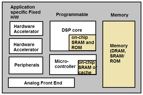 | Figure 1. Embedded memory architecture [1] |
2. Conventional DP SRAM
- Dual port RAM cells is used to achieve a higher RAM density. As each port must be able to access the cell independent of each other the basic access lines; bit line, bit line bar and word line need to be duplicated.There are two types of memory cells used for the DP SRAM, the 1-Read/Write (1-RW) memory cell and 2-RW memory cell [9]. Both of the memory cells have eight transistors (8T) in common. However, the drawback of 1-Read/Write is its single ended read bit line structure [6]. This paper focused in 2-RW cell type as shown in Figure 2 comprises two cross-coupled inverters (flip-flops) from M1 until M4 that are used to store the data, the rest M5 until M8 are used to access the stored data in the cell. 2-RW type as compared to 1-RW, both of the ports are able to do the read and write operation at the same time. Besides, it also can be operated as 1-RW type.
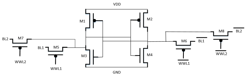 | Figure 2. Circuit diagram of 2-RW memory cell |
3. Low Power DP SRAM CMOS Design Techniques
- The conventional 2-RW cell has to be modified in order to observe the techniques that offer the most low power consumption and improve the performances of the DP SRAM. These techniques increased the number of the transistors in the low power design more than the conventional 2-RW cell.
3.1. Multi-threshold CMOS (MTCMOS)
- Low power and high stability has become the main issues in designing the SRAM. Therefore, by using the MTCMOS process, leakage current would be minimized and a large scale (macro) of SRAM are divided into multiple sub-macros to improve the read and write stability and ability and reducing the dynamic power. In MTCMOS technology, low, normal and high threshold voltage (Vt) transistor were used in designing a CMOS. Low-Vt (LVt) will give a high performance in the circuit design because the propagation delay could be reduced in the critical path and can be used whenever high performance is required. However, the LVt could caused the leakage current to be increased in the sub threshold. For the High-Vt (HVt) transistor, to be compared with the LVt, the HVt can be used to reduce leakage currents and the power consumption in the shortest path [7]. Mitra [10] proposed 8T 1-RW DP SRAM using MTCMOS technique in 90nm CMOS technology with power consumption of 1.71uW, read and write delay of 15.93ps and 8.9ps, respectively.MTCMOS power gating technique has been introduced in [3]. The sleep transistors that is applied between the supply voltage and the LVt gate, and between the ground line and the HVt device is known as “power gating”. The 9T SRAM in [3] consumed power of 88.22uW and propagation delay o and Figure 3 shows the MTCMOS with power gating technique. The sleep transistors will reduce the subthreshold leakage during sleep mof 340ps for 1-bit cell.
 | Figure 3. MTCMOS power gating technique |
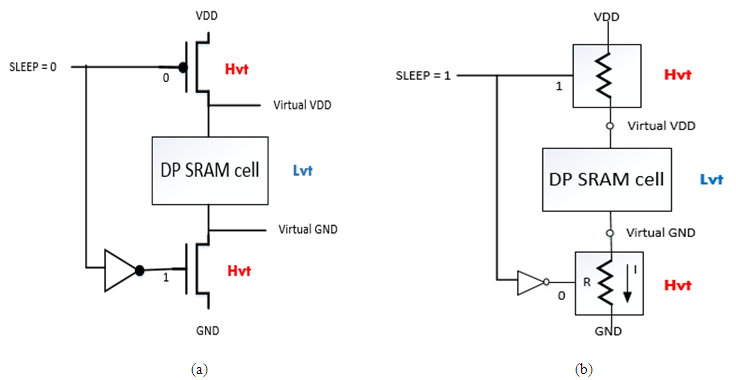 | Figure 4. Power gating; (a) during active mode; (b) during standby mode |
3.2. Full Stack CMOS (FSCMOS)
- Stack effect is the condition when two or more stacked transistors are turned off together, thus able to reduce the leakage power consumption [8]. Two PMOSs were stacked on the top of the pull-up transistors, M1 and M2 of the conventional memory cell and the other two NMOSs will be stacked at the bottom of pull-down network, M3 and M4. These PMOSs and NMOSs will be named as the PMOS stacking transistors and NMOS stacking transistors respectively. The reverse bias will be induced between the stacked transistors and the memory cell and the two cross-coupled inverters, thus resulting a lower sub-threshold leakage current. However, this would increase the delay and affect the circuit performances. Figure 5 shows the circuit diagram of FSCMOS technique. The working principle of memory cell in this technique were the same as the conventional memory cell. During both of word lines is inactive (0V), the flip-flops will be isolated with the access transistors, which will not allowing any read and write operation occurs. Therefore, node at ‘0’ value will be connected to the GND through the two series of pull-down network and NMOS stacking transistors. Similarly, at node ‘1’ value will be connected to the VDD (1V etc.) through the two series of pull-up network and PMOS stacking transistors. These will causes the leakage current reduction due to the stack effect. The power consumption in this technique could be further lowered by applying the HVt at the stacking transistors and normal-Vt (NVt) at the conventional memory cell. This could optimize both power consumptions and delay in the circuit.
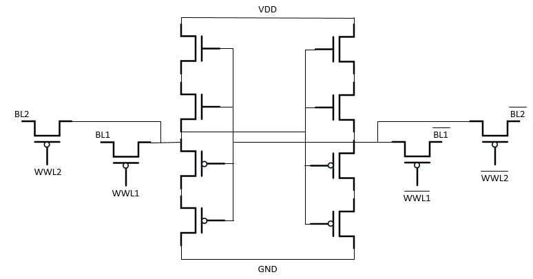 | Figure 5. FSCMOS technique |
4. Results and Discussions
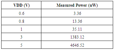
- DP SRAM circuit have been simulated at different voltage levels in range of 0.6V to 5V implemented in 0.25µm CMOS technology using Tanner Tools. Result showed that reducing the voltage level affecting the power consumption to be decreased. But as using 0.25µm CMOS technology, the minimum threshold voltage of the transistor might be higher for the voltage below 1V, the output waveform is degraded. Thus, 1V is chosen to be supplied in this memory cell. Table 1 shows the range of voltage supply of the circuit and its corresponding power consumptions.
|
|
5. Conclusions
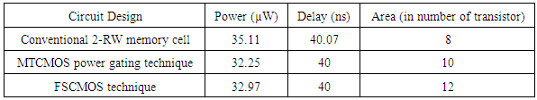
- As a conclusion, DP SRAM with MTCMOS power gating technique has proven to reduce the power consumption in a memory cell, and overall of DP SRAM design. Using FSCMOS also reduced the conventional DP SRAM but required more number of transistors used in the cell that cause larger area of SRAM design compared to the MTCMOS and conventional design. Time delay also has been measured and proved that by applying these low power techniques, the speed performances of the conventional DP SRAM could be improved. The delay measurement involves both process during read and write operation.
ACKNOWLEDGEMENTS
- This work was financial supported by Universiti Tun Hussein Onn Malaysia (UTHM). The authors would also like to thank Industry Centre of Excellence (ICoE), Faculty of Electrical and Electronic Engineering (FKEE), Silterra and Collaborative Microelectronic Design Excellence Centre (CEDEC).