Hassan Kaatuzian, Keyvan Farhang Razi
Photonics Research Laboratory (P.R.L), Electrical Engineering Department, Amirkabir University of Technology, Tehran, Iran
Correspondence to: Keyvan Farhang Razi, Photonics Research Laboratory (P.R.L), Electrical Engineering Department, Amirkabir University of Technology, Tehran, Iran.
| Email: |  |
Copyright © 2016 Scientific & Academic Publishing. All Rights Reserved.
This work is licensed under the Creative Commons Attribution International License (CC BY).
http://creativecommons.org/licenses/by/4.0/

Abstract
Conversion gain improvement of an integrated opto-electronic mixer consisting of InP/InGaAs heterojunction bipolar transistors(HBTs) in single and cascode configuration is estimated in this paper. The effects of two methods are analyzed for this purpose. Two important factors for determining the performance of a transistor are base transit time  and current gain(β). In first method, the uniform base doping profile is modified to nearly Gaussian base doping profile and by this modification base transit time is decreased and current gain is increased from 130 to 306. In second method, linear grading of composition of the base is proposed to enhance current gain and decrease base transit time. In second method current gain is increased from 130 to 292. Another important factor for determining performances of a transistor is base width. By decreasing base width up to 250 A, current gain can be increased up to 614 and 553 in first and second methods respectively. The dependence of diffusion constant, doping concentration and temperature is considered in the first method. The modified transistors are inserted in the structure of single and cascode Opto-Electronic mixers and after software simulation, considerable improvement of up and down conversion gains of mixer are obtained. It’s interesting to pay attention that, for the verification and calibrating software simulator, we’ve compared the simulation results of a typical HBT, before modifying it and compared with empirical reported experiments. Then we examined the simulator on our modified proposed HBT to prove its higher conversion gain.
Keywords:
HBT, Mixer, Opto-Electronic, Nearly Gaussian doping profile, Linear grading composition, Current gain, Base transit time
Cite this paper: Hassan Kaatuzian, Keyvan Farhang Razi, Conversion Gain Improvement of InP/InGaAs HBT Opto-Electronic Mixer Using Nearly Gaussian Doping Profile and Linear Grading of Composition in Base Region, Electrical and Electronic Engineering, Vol. 6 No. 2, 2016, pp. 30-38. doi: 10.5923/j.eee.20160602.03.
1. Introduction
The key property of an Opto-Electronic mixer is its nonlinear features. Due to this property, in the structure of studied mixer [1], InP/InGaAs HBTs are used. HBT OEMs exhibit better optical responsivity and due to their thicker optical sensitive layer and higher intrinsic gain of the photo induced current [1]. Generally, HBTs consisting of III-V compounds play effective roles in high frequency and power applications. Using InP technology instead of GaAs technology is on increase due to their perfect current handling capability and high speed performances. The main reason of this superiority is higher electron mobility of p type InGaAs base region. For obtaining more down and up conversion gain of HBT Opto-Electronic mixer, base transit time is decreased and current gain of HBT is increased. In order to reach better speed performances, base resistance should be reduced by high doping concentration and base-emitter and base-collector junction capacitances and tunneling leakage current should be reduced by low doping concentration. Because of that nearly Gaussian base doping profile is proposed in this paper.Nearly Gaussian base doping profile can satisfy preceding two requirements [2]. Moreover, linear grading of Indium content through the base can create build-in field which causes more reduction of base transit time and more increment of current gain. All of this improvements are obtained with frequency band width enhancement. Elements of equivalent circuit of HBT for this mixer are obtained by using [3]. The modified transistors are inserted in mixer structure and by simulating proposed mixer, conversion gain improvement is estimated. Finally, conversion gain diagram of designed mixer is compared with mixer of reference [1] and [5].
2. HBT Model and Mixer Configurations
Schematic diagram of epitaxial layers of InP/InGaAs HBT transistor that is used in mixer structure is shown in Figure 1.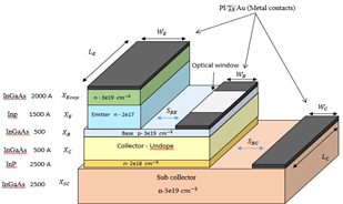 | Figure 1. Schematic diagram of epitaxial layers of HBT |
For modeling HBT in simulating software, a large signal model is employed. This model is shown in fig. 2 [1].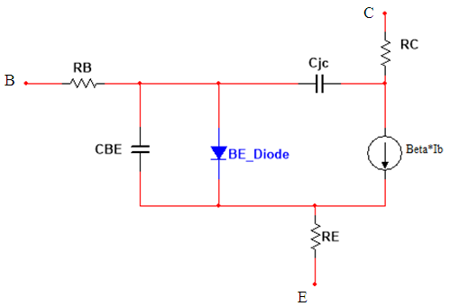 | Figure 2. HBT large signal equivalent circuit |
In this section elements of large signal model of HBT are explained. In model of Figure 2, two capacitors are inserted. HBT in a Opto-Electronic mixer is always in a forward-active mode, due to base-emitter diode is forward bias and base-collector diode is reverse bias. Because of that, base-emitter capacitor consists of depletion and diffusion capacitors and it is modeled by variable capacitor but base-collector capacitor consists of only junction capacitor and it is modelled by constant capacitor.Base-emitter diode that is shown in Fig. 2 is the most important element in large signal model of HBT because of its nonlinear property. This diode plays mixing role in structure of an Opto-Electronic mixer and mixes frequencies of optical and electrical section of the circuit.In order to have HBT with better characteristics, base resistor and capacitors should be decreased and current gain of transistor should be increased.If HBT with higher current gain is used in a Opto-Electronic mixer, up and down conversion gains can be improved obviously.Opto-Electronic mixer was built in single and cascode configurations. Schematic diagram of single configuration is depicted in Figure 3.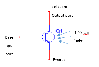 | Figure 3. Schematic diagram of single configuration of Opto-Electronic mixer |
Schematic diagram of cascode configuration of an Opto-Electronic mixer is shown in Figure 4.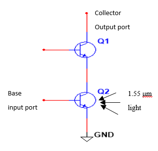 | Figure 4. Schematic diagram of cascode configuration |
A distributed feedback emitting at 1.55 μm was modulated by Mach Zender modulator. The modulated light was amplified by erbium doped fiber amplifier (EDFA) and then the light was focused on optical window that is located on base [1].
3. Base Transit Time and Current Gain Improvement of HBT, Using non Uniform Base Doping Profile
There are two key parameters that limit frequency response and current gain of HBT: base resistance and junction capacitance of base-emitter and base-collector.In order to reduce base resistance, base doping should be increased and in order to reduce junction capacitances and tunneling leakage current, base doping should be decreased.At a glance it seems that it’s impossible to benefit previous two advantages simultaneously but we will show that if base region of transistor is designed by nearly Guassian method, we can reach both goals at the same time.If base region is designed by linear grading of composition, it means that mole fraction of Indium in InGaAs varies linearly from base emitter junction to base collector junction, an internal electric field will be created and cause reduction in base transit time and enhancement of current gain.
3.1. Presenting Required Equations Associated with Current Gain and Base Transit Time Improvement
Base transit time of InP/InGaAs HBTs by Kroemer’s double integration is given by [6]: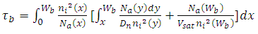 | (1) |
Where  is neutral base width,
  is the p type base doping concentration,
  is electron diffusion coefficient in base
  is the saturation velocity of minority carrier in base.Einstein’s equation is given:
 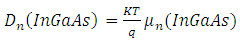 | (2) |
Where  is electron mobility in InGaAs base, K Boltzmann constant, T absolute temperature and q electronic charge.Mobility in InGaAs is related to mole fraction of Indium by equation (3) [6]:
 | (3) |
 is total Indium content in the base region.There is dependence between mobility, temperature and doping concentration and it is given by equation (4) [2]:
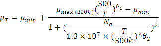 | (4) |
 is
is 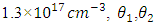 and λ are 1.59, 3.68 and 0.48 respectively. InGaAs
  and
and  are 300 and 14000
  respectively.Current gain of InP/InGaAS HBT is given [2]:
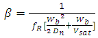 | (5) |
 is effective electron velocity through the neutral base region,
  is recombination factor and it is given by [4]:
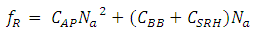 | (6) |
 is Augur coefficient for holes,
  is band to band radiative coefficient.
  is Shockely-Read-Hall coefficient.By solving integral from (1), base transit time’s equation can be written as (7) [4]:
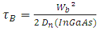 | (7) |
General form of non-uniform base doping profile is given by equation (8) [2]: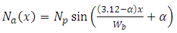 | (8) |
Where  and 0.1 ≤ α ≤ 1.57
 | (9) |
where  is base doping concentration near base-emitter junction and
  is maximum doping concentration through base region.Base doping profile is shown in Figure 5 for α=0.1 and α=1.57
 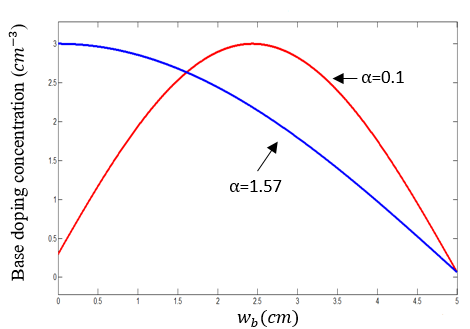 | Figure 5. Base doping profile for nearly Gaussian and continuosly decreasing doping |
When α=0.1 base profile is called nearly Gaussian profile and when α=1.57, base profile is called continuosly decreasing profile.The amount of doping concentration near junctions are related to α by equation (10) [2]. | (10) |
By using base doping profile of (8) exact equation of base transit time is obtained after solving (1) and it is given by equation (11).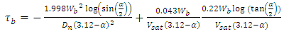 | (11) |
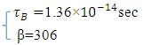
The first term inside bracket of (5) represents base transit time and by replacing (11) in (5) current gain for transistors with nonuniform base doping profile is obtained.Physical parameters of reference transistor that is shown in Figure 1 are given by Table 1.Base transit time and current gain of reference transistor are obtained by using information of Table 1 and equations (5) and (7). They are given below: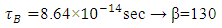 These amounts match completely with what were reported by [1]
Table 1. Physical parameters of reference transistor used in our simulation
 |
| |
|
3.2. Base Transit Time and Gain for Nonuniform Base Doping Profile without Considering Variation of Electron Diffusion Constant, through Base Region
We consider base doping profile like what was mentioned in (8) and using equations (5) and (11), base transit time and current gain are obtained for proposed transistor. In this section, we don’t consider variation of minority carrier concentration through base region. New transit time and current gain are given Base transit time and current gain depend on base width and this dependency is shown in Figure 6 and Figure 7.
 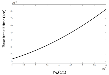 | Figure 6. Base transit time vs base width |
 | Figure 7. Current gain vs base width |
It’s observable from Figure 6 and Figure 7 that if base width is decreased, improvements in transit time and current gain will occur. But we have limitation for decreasing base width because of quantum effects such as punch through. Current gain can be increased to 591.3 by decreasing base width from 500 A to 250 A.
3.3. Base Transit Time and Current Gain for Nonuniform Base Doping Profile And Minority Carrier Diffusion Coefficient as Function of Doping Concentration and Temperature
Actually, when base doping profile is altered from uniform to nonuniform, electron carrier diffusion coefficient doesn’t remain constant and it varies through base region.Equation between mobility of base material (InGaAs) and absolute temperature and doping concentration presented in (12) [2]: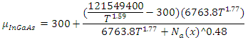 | (12) |
By considering (12) and solving (5) and (7) base transit time and current gain of modified transistor are calculated.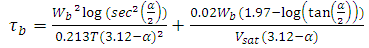 | (13) |
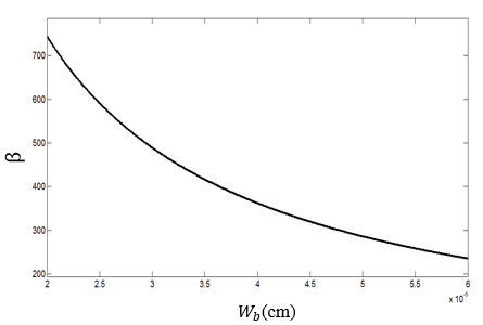
 We can see that current gain of transistor is enhanced from 130 to 306.Current gain alteration versus base width alteration in this method is demonstrated in Figure 8.
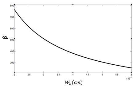 | Figure 8. Current gain vs base width |
If base width is reduced from 500 A to 250 A, without any quantum effects such as punch through, current gain can be increased to 614.
3.4. Base Transit Time and Current Gain for Nonuniform Base Doping Profile with Linear Grading of Composition in Base Region
In this method, energy gap of InGaAs base does not remain constant in entire base region because of linear grading of composition. Energy gap of InGaAs base is presented here. | (14) |
Where  is In mole fraction near base-emitter junction and
  is In mole fraction near base-collector junction. We can see that energy gap in the base region is function of position in linear way.For calculating base energy gap in each point, equation (15) is used.
 | (15) |
 is Indium mole fraction in each point. Base transit time in this method is obtained by solving (7) and considering (14) and (15) [2].
 | (16) |
For studied transistor base transit time and current gain are given. In this section, we set
  and
and  because of reference transistor’s structure. In this method like previous two methods, base transit time and current gain depend on base width and these dependences are shown in Figure 9.
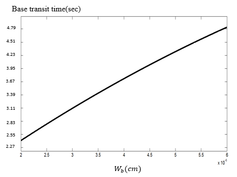 | Figure 9. Base transit time vs base width |
By reducing base width, base transit time is decreased and current gain is increased until quantum effects don’t occur. For example, for Wb = 250 A they are given.
3.5. Analyze Effects of Base Modifications of HBT on Elements of Equivalent Circuit
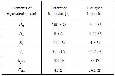
In this section we want to show effects of these modifications on elements of equivalent circuit shown in Figure 2.Elements of large signal equivalent circuit for empirical transistor and designed transistor are compared in Table 2. they are obtained by using [3] and all of the elements of empirical transistor in this model are conformed with what are reported by [1].Table 2. Comparison of elements of equivalent circuit
 |
| |
|
As it was shown in Table 2, we can see acceptable decrement of base resistance. Moreover, junction capacitances of base-emitter and base-collector are decreased.Decrement of these elements are the main reasons for base transit time and gain improvements.
4. Using Improved HBT in Structure of Opto-Electronic Mixer
In this section, we will use improved transistor that was designed in last section, in structure of Opto-Electronic mixer. Up and down conversion gain diagrams of empirical and designed mixers are compared by ADS software.
4.1. Designed HBT Opto-Electronic Mixer in Single Configuration
The large signal nonlinear model that is used for simulating of single configuration mixer is shown in Figure 10.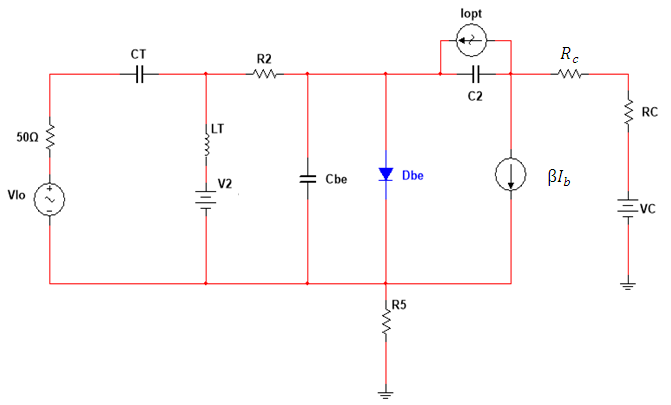 | Figure 10. Large signal nonlinear model of single configuration mixer |
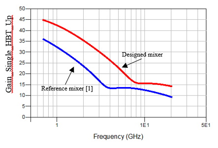
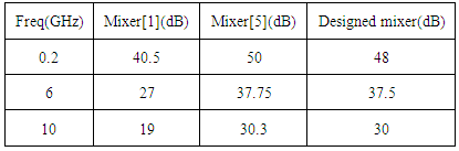
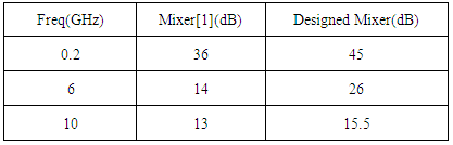
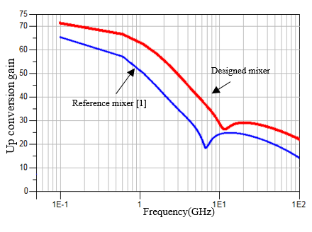
Down and up conversion gains of single Opto-electronic mixer as a function of optical modulation frequency are shown in Figure 11 and Figure 12. Designed mixer is compared with primary mixer in various optical modulation frequencies in Table 3 and Table 4. In figure 11 in addition to primary an designed mixers, mixer of reference [5] is shown. This mixer has different physical parameters from mixer of reference [1].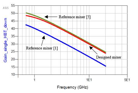 | Figure 11. Down conversion gain of single mixer as a function of optical modulation frequency |
 | Figure 12. Up conversion gain as a function of optical modulation frequency |
Table 3. Comparison of down conversion gains of mixers
 |
| |
|
Table 4. Comparison of mixers’up conversion gains
 |
| |
|
4.2. Designed HBT Opto-Electronic Mixer in Cascode Configuration
The large signal nonlinear model that is used for simulating of cascode configuration is shown in Figure 13.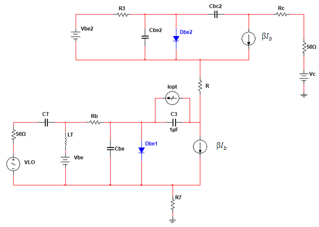 | Figure 13. Equivalent circuit for simulating Opto-Electronic mixer in cascode configuration |
Down and up conversion gains of opto-electronic mixers in cascode configuration as function of optical modulation frequency are shown in Figure 14 and 15.Improvement of down and up conversion gains in designed mixer is observable in Figure 14 and figure 15.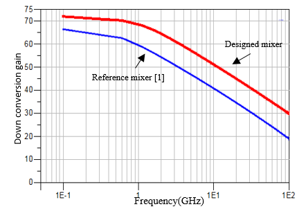 | Figure 14. Down conversion gain of mixers in cascode configuration as a function of optical frequency (ADS software simulation) |
 | Figure 15. Up conversion gain of mixers in cascade configuration as a function of optical frequency |
4.3. Importance of Obtained Results
The importance of these simulating results will become more obvious if we consider that conversion gain is improved without decrement of frequency band width. In ordinary situation if current gain is increased, frequency band width will be decreased but in this paper because of change in the design of transistor, both of these improvements obtained simultaneously.
5. Conclusions
In this paper, Inp/InGaAs heterojunction bipolar transistors that are used in Opto-Electronic mixers, are studied. For improving Opto-Electronic mixer characteristics such as down and up conversion gains, design of base region is modified in order to decrease base transit time and increase current gain.In these modifications, base doping profile is changed from uniform to non-uniform nearly Gaussian doping profile. As a result, the current gain of transistor is increased from 130 to 306.In second method of modification, linear grading of composition is used in base region and as a result, current gain of HBT is increased from 130 to 292. Then modified transistors are inserted in Opto-Electronic mixer structure and after simulation, considerable improvement in up and down conversion gains, are obtained. Moreover, it is clear from our results that frequency band width is improved simultaneously.
References
| [1] | Yoram Betser, “An integrated hetero junction bipolar transistor cascode opto-electronic mixer”, IEEE transactions on microwave theory and teqniques, Vol. 47, N0. 7, July 1999. |
| [2] | Pransejit Saha ; Sukla Basu, “A study of base transit time and gain of InP/InGaAs HBTs for uniform and nearly Gaussian base doping profile”, Journal of electron devices”, Vol.15, pp.1254-1259, 2012. |
| [3] | William Liu, Fundamentals of III-V devices, Wiley-Interscience, 1999. |
| [4] | Subhra Chowdhury, Sukla Basu, “Effect of device parameters on current voltage charecteristics and current gain of InP/InGaAs HBTs”, Journal of Electron Devices, Vol.9, pp.362-366, 2011. |
| [5] | Hassan Kaatuzian, Elahe Rastegar Pashaki, Hamed Ghodsi, Conversion gain improvement of HBT-Optoelectronic mixers using structural design alteration of device, SPIE Proceedings Vol. 9286, 2014. |
| [6] | P. Rinaldi, H. SchÄattler “Minimization of the base transit time in semiconductor devices using optimal control,” in Proc 4th Int. conf. Dynamical systems and differential equations, Wilmington, NC, USA 742-751, 2002. |

 Abstract
 Reference
 Full-Text PDF
 Full-text HTML