-
Paper Information
- Paper Submission
-
Journal Information
- About This Journal
- Editorial Board
- Current Issue
- Archive
- Author Guidelines
- Contact Us
Electrical and Electronic Engineering
p-ISSN: 2162-9455 e-ISSN: 2162-8459
2016; 6(2): 25-29
doi:10.5923/j.eee.20160602.02

Effective Elimination of Analog Impairments Error in Parallel Interleaving Sigma Delta A/D Converters
 Abstract
 Reference
 Full-Text PDF
 Full-text HTML
Tadeusz Sidor
University of Occupational Safety Management in Katowice, Poland
Correspondence to: Tadeusz Sidor, University of Occupational Safety Management in Katowice, Poland.
| Email: |  |
Copyright © 2016 Scientific & Academic Publishing. All Rights Reserved.
This work is licensed under the Creative Commons Attribution International License (CC BY).
http://creativecommons.org/licenses/by/4.0/

The oversampling sigma delta modulators which produce one bit samples of input signals can be used to create AD converters, which can produce either multi bit samples of high resolution but with low sampling frequency, or low resolution samples with high sampling frequency. One of the methods of overcoming this limitation is based on using several converters operating in parallel in a time interleaving manner. This way the resolution of the converter digital output can be significantly increased i.e. the quantising error value reduced. However the analog impairments of parallel converters cause modulation of the output samples which can significantly deteriorate the resultant converter properties. Somehow in many papers describing various structures of Σ-Δ AD converters analysis is limited to the frequency domain, ignoring the fact that Σ-Δ modulators are in fact synchronous voltage to frequency converters. This paper demonstrates how, recognizing the time domain properties of Σ-Δ modulators, the problem of analog impairments of converters can be overcome resulting in a better design of high resolution Σ-Δ AD converters.
Keywords: Parallel sigma delta converters, Resolution, Sampling, Interleaving techniques
Cite this paper: Tadeusz Sidor, Effective Elimination of Analog Impairments Error in Parallel Interleaving Sigma Delta A/D Converters, Electrical and Electronic Engineering, Vol. 6 No. 2, 2016, pp. 25-29. doi: 10.5923/j.eee.20160602.02.
Article Outline
1. Introduction
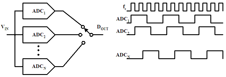
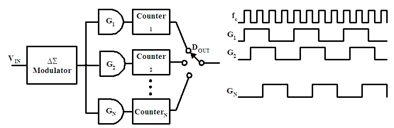
- The sigma-delta (Σ-Δ) AD converters are nowadays the most popular choice employed in digital audio systems and in high-resolution precision industrial measurement. In the digital audio systems the flat distribution of quantising error, achieved by using sigma delta modulators of higher order, is relevant as it eliminates the idle tones which appear in the audio outputs. Therefore, taking into consideration the distribution of quantising errors, the majority of existing papers presents analysis of various Σ-Δ AD converters in frequency domain ignores the time domain properties of Σ-Δ modulators. However in the industrial digital system only the magnitude of quantising error is important, and taking this into consideration the Σ-Δ modulators can be viewed [1] as a synchronous voltage-to-frequency converter followed by a counter. If the number of "1"s in the output data stream is counted over a sufficient number of clock pulses, the counter output will represent the digital value of the input.Remembering this, the relevant improvement of properties of the parallel structure Σ-Δ AD converters can be achieved, what is presented in this paper.Generally the main advantage of Σ-Δ AD converters is that the digital output of them can be of very high, theoretically unlimited, resolution. However to obtain high resolution of the output digital words the counting time requires many clock pulses which results in a low sampling rate. Using a single Σ-Δ converter, of any order, it is not possible to have both high resolution and high sampling rate. The idea was then conceived to provide additional samples in between high resolution samples by using additional Σ-Δ converters working in parallel.Many concepts of parallel Σ-Δ converters have been described in the literature [2], [3], [4], [5]. The majority of these basically rely more or less on the concept of interleaving ADCs described in [8].A block diagram showing the basic idea of such a parallel converter is shown in Fig. 1.
 | Figure 1. An array of N time interleaved n-bit ADCs [1] |
 and
and  is the clock pulse duration, and begin converting it again into an n-bit digital representation. Then, another T seconds later, ADC3 will sample VIN at (t0 + 2T) and so on. Before ADCN has finished sampling it started at (t0+NT), ADC1 at [t0+(N+1)T] immediately restarts sampling and the whole cycle of sampling is repeated.As the n-bit outputs of the ADCs become sequentially available, the digital n-bit samples sequentially appear at the converter output DOUT.If the fixed conversion time of each individual ADC is denoted by M, then if only one ADC operates in the system the sampling rate equals 1/M. When N interleaved ADCs operate in the described above manner, the effective sampling rate is N times higher i.e. N/M.This powerful technique makes possible a significant increase in the sampling rate of the Σ-Δ AD converter whilst keeping high converter resolution. However the interleaving technique is not free of practical challenges, as described in [8]. The analog impairments in the numerous channels of ADCs cause modulation of the output samples, leaving “interleaving spurs”, which are equivalent to the presence of additional components in the output signal spectrum. The spectral degradation of the output does not depend on the absolute value of the channels’ impairments (amplifiers gain and offset), but on the relative mismatches/differences between them. The timing spurs, which might appear, when the consecutive channels sample a bit earlier or later than they should in the intended order, can be eliminated by using single clock to operate all of the converters, but there is no effective solution to eliminate problems caused by the analog impairments of the channels if more than one Σ-Δ modulator is used in parallel AD converter.To illustrate how the analogue impairments of Σ-Δ AD converters cause modulation of the output train of samples Fig. 2 presents case of only two converters working in parallel.
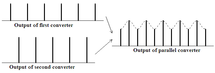 | Figure 2. Analogue impairments (gain) of two Σ-Δ AD converters, working in parallel cause magnitude modulation of the output train of samples |
2. Theoretical Consideration
- Let us consider the structure of a single channel of a typical Σ-Δ AD converter in the form shown in Fig.3 which is commonly used [9].
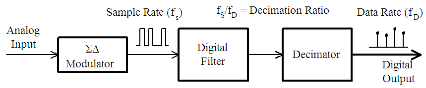 | Figure 3. Block diagram of typical structure of a single channel of a Σ-Δ AD converter presented in literature [4, 5] |
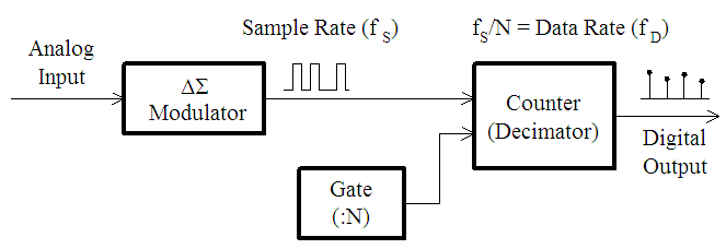 | Figure 4. Simplified block diagram of a single channel of a Σ-Δ AD converter with digital filter and decimator replaced by series input parallel output counter |
 | Figure 5. Modified structure of the array of N time interleaved n-bit ADCs |
3. Results of Verifying Simulation
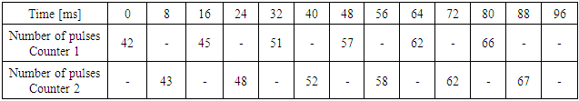
- For practical reasons simulation of very limited case has been presented. An example of only two interleaved counters was analyzed, but more counters can be added and their maximum number would be when they are interleaved by one clock pulse only. However for the converter resolution of e.g. 22 bits it would be the prohibitive number of 4194304 counters.Using Microcap [11] circuit simulator, simple 1st order Σ-Δ Modulator action was simulated, using a slowly rising ramp voltage as input source. The output pulses of the modulator were recorded and stored in a file. Simulating counter action, the number of output pulses was counted during 64 clock pulses starting from zero time. It was equivalent to the production of 6 bits samples with 16 ms sampling interval. Again it is very low converter resolution but increasing it to e.g. 22 bits would increase dramatically simulation time. The decimal values of consecutive samples are presented in Table 1.
|
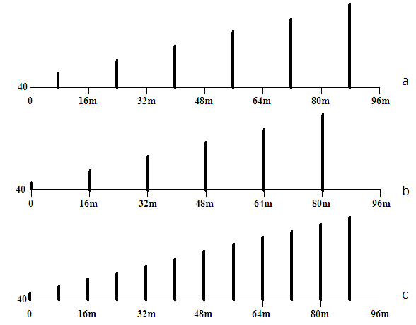 | Figure 6. Samples of simulated action of Σ-Δ ADC with single Σ-Δ modulator and two time interleave counters |
4. Conclusions
- For practical reasons an example of only two interleaved counters was given above, with very low resolution of only 6 bits, but more counters can be added and their resolution increased by extending the counting time. It is thus theoretically possible to obtain multi-bit samples with high sampling frequency which theoretically can equal the frequency of the Σ-Δ modulator clock. The possibility of increasing the sampling frequency by adding interleaved counters can be used to increase the number of bits in the samples above the necessary limits.It would be possible to use modulators of lower order. Contemporary Σ-Δ AD converters employed in acoustic devices use modulators of order as high as fifth to limit the appearance of idle tones caused by the periodic appearance of quantizing errors. It is well known that using a modulator of order higher than second causes the modulator circuit to become unstable and special techniques should be used to prevent this. By using modulators of lower order and increasing the number of bits in the samples above the necessary limits it is possible simply to reject LSB and eliminate totally the periodic components of quantising error which causes the problem of idle tones in acoustic devices.