-
Paper Information
- Previous Paper
- Paper Submission
-
Journal Information
- About This Journal
- Editorial Board
- Current Issue
- Archive
- Author Guidelines
- Contact Us
Electrical and Electronic Engineering
p-ISSN: 2162-9455 e-ISSN: 2162-8459
2016; 6(1): 6-10
doi:10.5923/j.eee.20160601.02

Design and Fabrication of Super Junction MOSFET for Industrial Applications
 Abstract
 Reference
 Full-Text PDF
 Full-text HTML
Ey Goo Kang
Department of Photovoltaic Engineering, Far East University, Korea
Correspondence to: Ey Goo Kang, Department of Photovoltaic Engineering, Far East University, Korea.
| Email: |  |
Copyright © 2016 Scientific & Academic Publishing. All Rights Reserved.
This work is licensed under the Creative Commons Attribution International License (CC BY).
http://creativecommons.org/licenses/by/4.0/

In Super Junction (SJ) MOSFET, Charge Balance is the most important issue of Trench filling SJ fabrication process. In order to achieve the best electrical characteristics, the N type and P type drift regions must be fully depleted when the drain bias approaches the breakdown voltage, called Charge Balance condition. In this paper, two method of the fabrication process are used in Charge Balance condition, Trench angle decreasing and Bottom implantation process. Smaller on-resistance can be achieved using lower trench angle. And higher Breakdown voltage can be achieved using Bottom implantation process. Electrical characteristics of manufactured discrete device chip are compared to that of device which is designed of TCAD simulation.
Keywords: Super Junction MOSFET, Charge Balance, Trench angle, Bottom implantation, Power Device
Cite this paper: Ey Goo Kang, Design and Fabrication of Super Junction MOSFET for Industrial Applications, Electrical and Electronic Engineering, Vol. 6 No. 1, 2016, pp. 6-10. doi: 10.5923/j.eee.20160601.02.
Article Outline
1. Introduction
- Power semiconductor devices that use silicone elements have become an important aspect of the power consumption of automobile and electrical products. As a result, it has prompted research into the critical nature of silicone. The power semiconductor device has a trade-off relationship between on-resistance and breakdown voltage, which leads to a need for optimization during the design process. However, the value of the breakdown voltage is standardized according to the application of each element, so it needs to be designed to reduce on-resistance. The Super Junction MOSFET, which is applied to the structure of the Super Junction, achieves a higher breakdown voltage when the charge balances of the P area and N are equal, which results in a depletion of all areas. This raises the concentration of the N pillar, which allows for a significantly lower on-resistance value compared to the former designs [1]. The prior Super Junction structure had a CoolMOSTM that was produced using the multi-epi process [2, 3]; however, when the Super Junction MOSFET was made with trench filling, which can make the P-pillar area tighter and deeper [4] compared to the prior Super Junction, which was made using the multi-epi process, it was able to accurately match the charge balance, which maximized the special characteristics of the element. Unlike the multi-epi process, the Super Junction MOSFET, which was made using the trench-filling process, has an adjusted trench angle, which gives better resistance. In addition, the Super Junction MOSFET, which was made using the trench-filling process, can achieve a P pillar depth greater than the etched depth. This greater depth results from using bottom implantation on the lower part of the P pillar before it is filled during the P pillar trench etching. Because of this, a higher breakdown voltage than expected during design can be achieved, and by using this, N pillar’s concentration can be raised, which results in a lower on-resistance value than the prior elements that did not implement the bottom implantation. In this thesis, the change in the trench angle and Super Junction MOSFET implemented with the bottom implantation is planned out through simulation, the elements are produced, and the production data and simulation data are compared.
2. Electrical Characteristics of Super Junction MOSFET
2.1. Analytic Model for Charge Balance in Super Junction MOSFET
- In the Super Junction MOSFET, maximum breakdown voltage is achieved when the charge balance of both N pillar and P pillar are equal, according to the theory. When the width of the P pillar and N pillar are equal, the charge balance can be expressed as CD [%], and is represented in equation (1).
 | (1) |
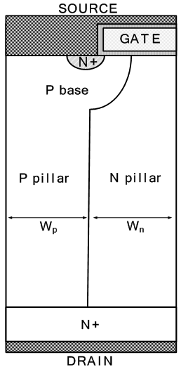 | Figure 1. Structure of Super Junction MOSFET |
2.2. Super Junction MOSFET’s Change in Electric Characteristics due to the Trench Angle’s Effect
- The Super Junction MOSFET that is formed through the trench-filling process is in the spotlight because the unit price for production is cheaper than the multi-epi process and it is easy to obtain uniform P pillar concentration. It is also easy to develop a high aspect ratio structure [4]. One of the important parameters when a Super Junction MOSFET is formed using the trench-filling process is the trench angle. By changing the trench angle, the breakdown voltage and heat resistance characteristics all change. Therefore, to confirm the change in electrical properties due to the trench angle, a simulation was done with the data of 600V Super Junction MOSFET using the etching angle of the trench shown in Figure 1. The structure’s half-cell pitch is 6.5µm, and P pillar and N pillar’s width are 3.25µm. The dose amount of P base is 6.5·1013cm-2 and N pillar’s ND concentration was set at 4.73·1015cm-3, while P pillar’s concentration NA was changed from 4.43·1015cm-3 to 6.13·1015cm-3. As seen in Figure 2, the change in breakdown voltage of the charge balance graph, the axis of the charge balance moves according to the trench angle. Plus, as the trench angle reduces, the charge balance point, or the breakdown voltage’s optimal value is also lowered. As the trench angle reduces the P pillar of the actual element, the charge amount of the area is reduced. Naturally, the breakdown voltage point of the charge balance is N, so the charge amount of P pillar becomes the same value and, therefore, is lowered.
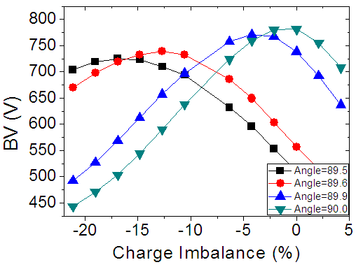 | Figure 2. Breakdown Voltage Characteristics of Trench Angle |
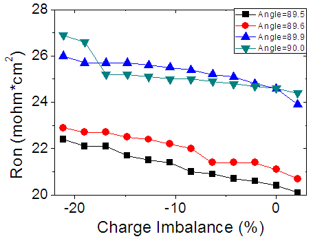 | Figure 3. On-resistance Characteristics of Trench Angle |
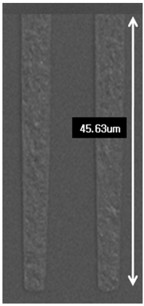 | Figure 4. SEM Picture of 89.5° P Pillar Trench Filling |
2.3. Bottom Implantation Process in Trench Filling Super Junction MOSFET
- The P pillar depth has a limit because the Super Junction MOSFET that has been made by the trench-filling process has a trench depth with a processing side that cannot be over the aspect ratio of a side able to be trench etched [5]. The bottom implantation was applied to cope with this depth limit. The flow of this process has been shown in Figure 5. Before the trench-filling process was developed, boron was doped into the bottom areas after trench etching, which allowed for a depth deeper than the past P pillar depths. In Figure 5 (a), N epi area’s trench was etched, and SiO2 was depositioned to use as a mask in a case of bottom implantation. This SiO2 deposition is seen from the top, so it is thicker than what was really depositioned. Because of this, the implantation is done to the trench wall and used as a layer to prevent the reduction of characteristics. This oxide is used to reduce one mask during bottom implantation. Afterwards, when implantation takes place in process (c), boron is also implanted in the top of N-epi. Because this causes the characteristics of the element to be impeded, after implantation, the trenched insides are filled with P doped silicon, the doped top of the element is ground with CMP and the contaminated top part is removed, so the bottom-implanted P pillar development process is complete. It was designed by implementing the bottom implantation on the design using the optimized trench angle.The values for the oxide thickness, implantation energy, and the implantation dose used in bottom implantation were ones that could be used in variations. As a result, according to the simulation, the depth was 48 μm compared to the past value of 46 μm. Also in terms of the electrical characteristics, the breakdown voltage characteristics rose from 671V to 690V, and the on-resistance characteristics changed from 21mΩ∙cm2 to 22mΩ∙cm2. It was confirmed that through the implementation of bottom implantation, the electrical characteristics improved. The modified SEM picture of Figure 5 is shown in Figure 6. As shown in Figures 7 and 8, the Figure 5 (d) process before CMP’s SEM can be shown in Figure 7 and the smooth surface of the element structure can be seen in Figure 8. In the next paragraph, the trench-angle characteristics shown in the last example and the bottom implantation process were implemented and data that made the 2A element chip was used to analyze and compare with the simulation.
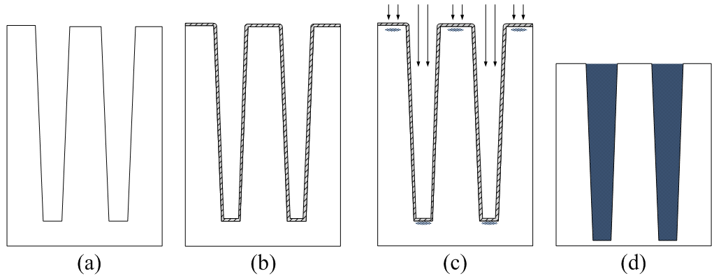 | Figure 5. Bottom Implantation Process in Super Junction MOSFET |
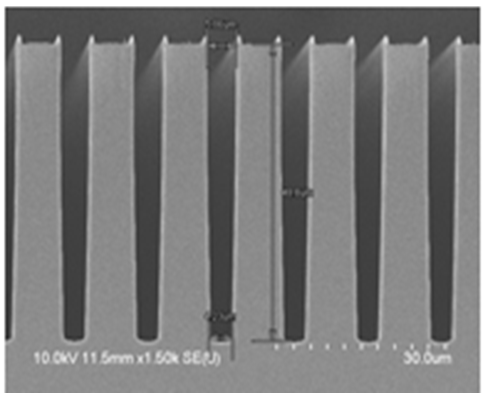 | Figure 6. SEM Pictures of Trench Etching |
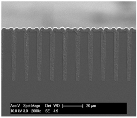 | Figure 7. SEM Pictures of Trench Filling |
3. Super Junction MOSFET Chip Data
3.1. Manufactured Trench Filling Super Junction MOSFET
- Using the simulation’s proved data (from the paragraphs above) as a base, the element was produced. As seen in the layout picture in Figure 8, 1 chip’s total area is 3180 μm • 2720 μm. Apart from the active layer, the edge termination part was made using a 600V level Super Junction fieldring. The electrical characteristics of the element were measured and were compared to the data before production.
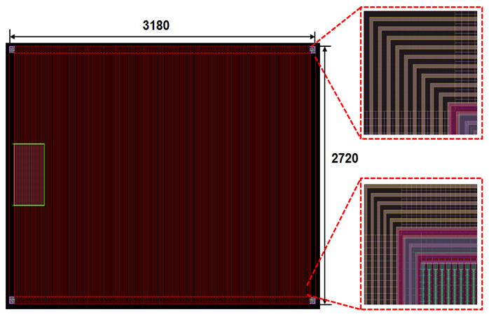 | Figure 8. 600V/2A Super Junction MOSFET Layout |
3.2. Analysis and Domparison of the Simulation Data and Measured Data
- The electrical characteristics of the chip (described above) were measured and compared to the simulation data from before production. As shown in Figure 9, the breakdown voltage characteristic’s base data used bottom implantation and trench-angle characteristics, and was made with 690V data, but the chip’s breakdown voltage was 667V, creating a 5% margin in the data. The on-resistance data of the simulation was 21mΩ∙cm2 and the measured data was 22mΩ∙cm2, which had a 4% difference. In terms of the production of an actual power semiconductor device, there is a 10% margin; therefore, the chip allows for accurate readings of breakdown voltage and on-resistance.
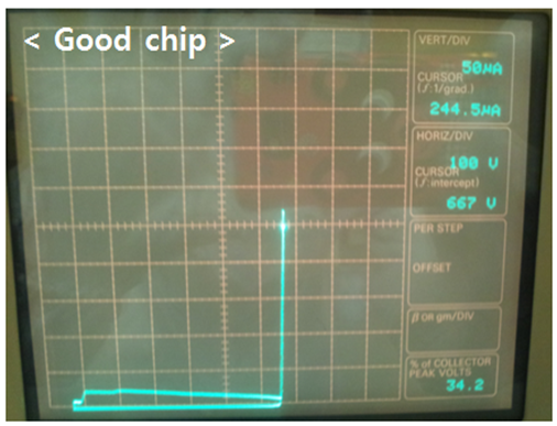 | Figure 9. Breakdown Voltage Measurement of 600V/2A Trench Filling Super Junction MOSFET |
4. Conclusions
- An important parameter of producing Super Junction MOSFET using the trench-filling process is that as the trench-angle value decreases, the on-resistance value also decreases. The lowest on-resistance value was found through simulation by using an 89.5° etch angle. Also, the limitation of the aspect ratio was a disadvantage of the trench-filling process, which limited the P pillar depth. Because of this the bottom implantation was implemented, and the P pillar increased along with the breakdown voltage. The discrete device chip was created using a simulation that implemented both sides, and when the breakdown voltage characteristics were measured, they showed an approximate 5% error rate. Because the margin of error of the power semiconductor device during planning was 10%, it showed that this chip was serviceable. In further research, the variables and their changes when using bottom implantation, as well as their electrical characteristics, will be examined and analyzed.