-
Paper Information
- Paper Submission
-
Journal Information
- About This Journal
- Editorial Board
- Current Issue
- Archive
- Author Guidelines
- Contact Us
Electrical and Electronic Engineering
p-ISSN: 2162-9455 e-ISSN: 2162-8459
2014; 4(4): 73-79
doi:10.5923/j.eee.20140404.02
Absorption Bandwidth-Enhanced Metamaterial Absorber Using In-planed ELC Resonator and Cut-Wire
 Abstract
 Reference
 Full-Text PDF
 Full-text HTML
H. M. Lee
Department of Electronic Engineering, Kyonggi University, Suwon, Korea
Correspondence to: H. M. Lee, Department of Electronic Engineering, Kyonggi University, Suwon, Korea.
| Email: |  |
Copyright © 2014 Scientific & Academic Publishing. All Rights Reserved.
In this paper, we present the design, fabrication, and characterization of a broadband metamaterial (MM) absorber, which consists of a lumped-resistor-loaded electric-inductive-capacitive (ELC) resonator and a cut-wire strip on the same side of the dielectric substrate. A metallic pattern layer of the proposed absorber is designed in parallel to the incident wave propagation direction. In contrast to a common ELC resonator, the lumped-resistor-loaded ELC resonator exhibits a switchable resonant mode behavior, thereby exhibiting a negative effective permeability (μeff < 0). In addition, this resonator exhibits a low quality (Q)-factor owing to the loaded lumped resistors, which enhances the absorption bandwidth of an MM resonator. Our experiments showed that the proposed absorber exhibits a peak absorption rate of 91% at 8.87 GHz, and 2.8 GHz of a full-width at half-maximum (FWHM) bandwidth is achieved.
Keywords: Absorber, Cut-Wire, Effective Medium, Electric-Inductive-Capacitive (ELC) Resonator, Metamaterial
Cite this paper: H. M. Lee, Absorption Bandwidth-Enhanced Metamaterial Absorber Using In-planed ELC Resonator and Cut-Wire, Electrical and Electronic Engineering, Vol. 4 No. 4, 2014, pp. 73-79. doi: 10.5923/j.eee.20140404.02.
Article Outline
1. Introduction
- Meatamaterials (MMs) can be represented by the complex values of electric permittivity εeff (= ε′ + jε″) and magnetic permeability μeff (= μ′ + jμ″). These complex values can be independently controlled by varying the dimensions of the electric and magnetic components. Additionally, the impedance of an MM can be well-matched to that of free space by tuning the electric and magnetic resonances. As a result, 100% absorption can be theoretically achieved. The configuration of the previously reported MM absorbers can be categorized into two types: absorbers with a metallic backing plate and metallic backplane-less absorbers. Most of the MM absorbers are equipped with a metallic backing plate [1–5] to avoid power transmission on the other side of the absorbers. However, the presence of backing plates is disadvantageous in stealth and camouflage applications [6]. The configuration of the previously reported metallic backplane-less MM absorbers involves the realization of two metallic patterns with the negative real parts of permittivity and permeability. The two metallic pattern layers separated by a dielectric spacer are designed orthogonally to the electromagnetic (EM) wave propagation direction [7–11]. In this case, the radar cross-section (RCS) of the metallic pattern expands at frequencies other than the targeted absorption frequency bands. Therefore, there is a need for a metallic pattern layer of the MM absorber to be designed in parallel to the EM wave propagation direction to avoid this problem. In our previous study, an MM absorber was designed by combining two open complementary split-ring resonators (OCSRRs) with a split-ring-resonator (SRR) separated by a dielectric substrate, and the metallic pattern layers were designed in parallel to the EM wave propagation direction [12]. Although, this structure serves as a dual-band MM absorber in the microwave frequency region, the absorption bandwidth of this MM absorber is quite narrow. This narrow bandwidth characteristic limits the absorber applications. Considering the fact that lumped elements can be used for enhancing the resonance bandwidth of an MM resonator [13], we present a new type of an MM absorber. The proposed MM absorber, which is designed by combining a lumped-resistor-loaded electric-inductive- capacitive (ELC) resonator and a cut-wire strip on the same side of the dielectric substrate, exhibits a broadband absorption characteristic. The proposed MM absorber structures are simulated using 3D field simulation tool, CST MWS (Micro Wave Studio).
2. Operating Modes of ELC Resonators
- An ELC resonator, which does not require continuous electrical connections between the unit cells, was first proposed as an alternative to a thin metallic wire, and it strongly couples to a uniform electric field [14]. This ELC resonator structure is composed of two SRRs positioned back to back. A variant ELC resonator structure comprises two capacitive gaps on the exterior of an inductive arm [15]. Both the ELC resonators, unlike SRRs, possess a high level of symmetry and do not exhibit a magneto-electric coupling behavior. With regard to the equivalent circuit, the ELC resonator can be considered as an LC circuit, where L and C are the geometric inductance and capacitance of the ELC structure, respectively. The incident EM field induces parallel and antiparallel magnetic dipoles in the two individual SRRs in each unit cell of the circuit, which correspond to symmetric and anti-symmetric modes, respectively [16]. Figure 1 illustrates the schematic and equivalent circuit of the two ELC resonators for symmetric and anti-symmetric modes. In the symmetric mode, the induced surface current components on the middle capacitive arm are out of phase, as shown in Figure 1(a). Therefore, the induced surface currents circulate around the outer edges of the ELC resonator. The symmetric mode originates from the magnetic coupling to the resonator, in which the effective permeability can be negative (μeff < 0). However, in the case of the ELC resonator comprising two SRRs positioned back to back, the effective permeability is not negative (loop current mode). In the anti-symmetric mode, the induced surface current components on the middle capacitive or inductive arm are in phase, as shown in Figure 1(b). Therefore, the induced surface currents almost converge on the middle capacitive or inductive arm owing to the strong electric coupling, which contributes to the negative effective permittivity (εeff < 0).
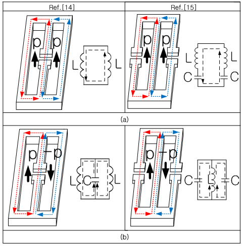 | Figure 1. Schematic and its equivalent circuit of an ELC resonator. (a) Symmetric mode. (b) Anti-Symmetric mode. The arrows (black color) in the ELC resonator indicate parallel or anti-parallel dipoles by inducing circulate surface currents (red and blue color) |
3. MM Absorber Design with In-planed Resonators
- We have designed an in-planed MM absorber by combining an ELC resonator and a cut-wire strip on the same side of the dielectric substrate, as shown in Figure 2(a), and simulations are carried out. The ELC resonators comprise a single metallic pattern layer etched on a Rogers R4003C dielectric substrate, which has a relative dielectric constant εr of 3.37, loss tangent δ of 0.003, and thickness t1 of 1.5 mm. Copper, with a conductivity σ of 5.8 × 10⁷ S/m, is used for designing the metallic patterns. In the simulations, the incident EM wave illuminates the proposed MM absorber with a parallel polarization, where the magnetic field H being normal to the ELC resonator and the electric field E coupled to the capacitive element, as shown in Figure 2(a).The periodic boundary conditions are applied to the top, bottom and two side walls of the waveguide. The other two opposite sides of the waveguide is assigned as open-waveguide ports, as shown in Figure 2(b). The lumped-resistor-loaded in the ELC resonator changes the resonance characteristics of the MM absorber. We simulate the proposed MM absorber structure for various values of the lumped resistors loaded within the ELC resonator to derive the optimum resistor value R, and the simulated impedance loci of the MM absorber over a frequency range of 8–12 GHz are shown in Figure 3. The marker numbers inside the impedance loci on the Smith chart indicate the points where the frequency is 8.95 GHz for various values of the lumped resistors loaded within the ELC resonator. When the lumped resistor value R = 910Ω, the input impedance of the proposed MM absorber is 371–j8 at 8.95 GHz. This impedance of the proposed MM unit cell is well-matched to that of free space (≈ 377Ω). When the lumped resistor value R > 910Ω, the quality (Q) factor of the ELC resonator will further reduce. However, the resonator is over-coupled to free space.
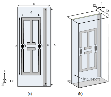 | Figure 2. (a) In-planed MM absorber unit cell consists of an ELC resonator and a cut-wire strip with following geometric dimensions: a= 4.3 mm, b= 9.2 mm, c=6.9 mm, d= 2.5mm, e=9.0 mm, t1= 1.5 mm, t2=1.5 mm and R=910 ohm. (b) Simulation set-up |
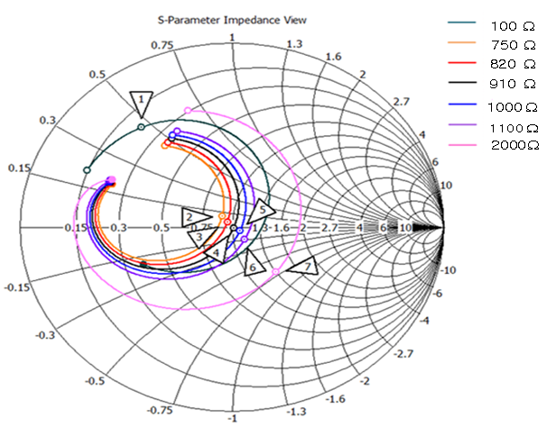 | Figure 3. Simulated input impedance loci for various values of the lumped resistors loaded within the ELC resonator |
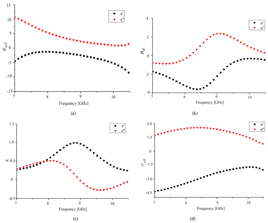 | Figure 4. Effective medium parameters of the MM absorber extracted from the scattering parameters: (a) effective permittivity, (b) effective permeability, (c) normalized impedance and (d) effective refractive index |
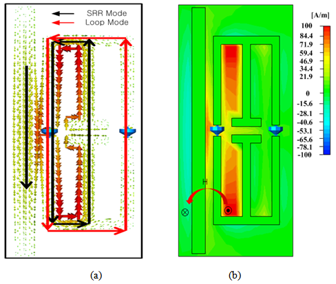 | Figure 5. Simulation results for the MM absorber at resonant frequency of 8.95 GHz: (a) surface current distribution and (b) magnetic field distribution |
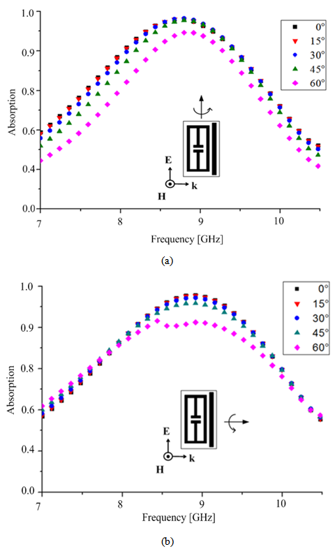 | Figure 6. Simulated results of the absorption curve for oblique incident angle dependence: (a) TE polarization Surface current distribution and (b) TM polarization |
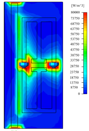 | Figure 7. Distributions of average power loss density in the proposed MM absorber |
4. Comparison of Different Types of MM Absorbers
- To compare the effects of lumped resistors in ELC resonator, three different configurations of the in-planed MM absorbers are numerically investigated, as shown in Figure 8. The simulated results are listed in Table 1. For comparison purpose, an in-planed MM absorber with an ELC and a cut-wire (Type 1) is designed. In Type 3, single SRR is used in place of the ELC whereas the dielectric substrate is removed from the edges of the ELC in Type 2.
|
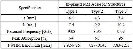
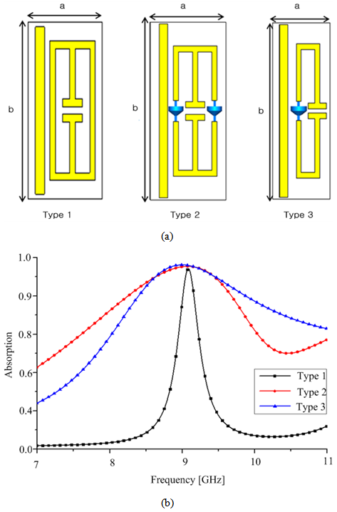 | Figure 8. Simulated results for three different MM absorbers: (a) three different types of in-planed MM absorbers and (b) comparison of absorption for three different MM absorbers |
5. Measurement Results
- We have fabricated a prototype MM absorber sample for an experiment to verify the effectiveness of the MM absorber. The photographs of the fabricated single-layer metallization MM absorber strip samples are shown in Figure 9 (a). The sample is etched on a Rogers R4003C substrate using standard photolithography techniques. The lumped resistors (resistance R = 910 Ω, 1005-type thick film with a size of 1.0 × 0.5 mm) are loaded on the inductive arms of the ELC resonators by applying the surface-mount soldering technology. A single period of the absorber strip consists of 70 unit cells etched on one side of a dielectric substrate. The absorber strips, each of which comprises an ELC resonator and a cut-wire strip configuration, are vertically aligned in parallel to the wave propagation direction. The inter-element spacing between the two vertically aligned absorber strips is set to 3 mm, and a silicon rubber substrate which has a relative dielectric constant εr of 3.37, and loss tangent δ of 0.001 is inserted between the absorber strips. The total size of the planar absorber with a planar array of absorber unit cells (33 × 70) is 312 × 303.6 mm. We have experimentally verified the behaviour of the absorber by measuring the S-parameters of the planar array of unit cells. Measurements are performed over a frequency range of 7.5–10.5 GHz using a vector network analyzer (Agilent Technology E5071C), and two X-band standard gain horn antennas (Model: 16240, Flann Microwave Instruments) are used to transmit the EM wave on the sample absorber sheet and to receive both the reflected and the transmitted signals to measure the absorption rate at normal incidence.
 | Figure 9. (a) Photographs of the fabricated prototype absorber strip samples and (b) absorption measurement set up with horn antenna |
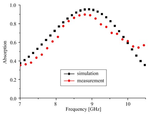 | Figure 10. Calculated and measured absorption rate of the MM absorber at normal incidence |
6. Conclusions
- We have designed, simulated, and experimentally verified a new type of a backplane-less MM absorber configuration. A metallic pattern layer of the proposed absorber is designed in parallel to the incident wave propagation direction. The main effects of the lump resistor on the ELC resonator are lowering the Q-factor of the resonator and exhibiting a negative effective permeability (μeff < 0). We have fabricated a prototype absorber with a planar array of 33 × 70 unit cells and experimentally verified the performance of the proposed absorber. The experimental results demonstrate that the composite MM absorber comprising an ELC resonator loaded with lumped resistors and a cut-wire strip configuration exhibits a wider absorption bandwidth than the previously designed MM absorber with an ELC resonator. The results of our study show that the design of the proposed absorber configuration can be easily extended to the design of more compact, thinner backplane-less planar absorbers for mm-wave and terahertz-frequency applications.