Electrical and Electronic Engineering

p-ISSN: 2162-9455    e-ISSN: 2162-8459

2014;  4(3): 45-51

doi:10.5923/j.eee.20140403.01

Effect of on Resistance Modulation in RF Switches Linearity

Christopher Liessner, Samson Mil’shtein

Electrical and Computing Engineering, University of Massachusetts, Lowell, USA

Correspondence to: Christopher Liessner, Electrical and Computing Engineering, University of Massachusetts, Lowell, USA.

Email:

Copyright © 2014 Scientific & Academic Publishing. All Rights Reserved.

Abstract

Radio frequency (RF) switch modeling has evolved as semiconductor processes have been developed and refined. However, to date no modeling has included the effect of the variation of the resistance of a switch on its linearity when the switch is in the on state. This paper presents an analysis that predicts the effect on signal linearity when the series resistance is modulated.

Keywords: FET switch, Linearity, pHEMT switch, RF switch

Cite this paper: Christopher Liessner, Samson Mil’shtein, Effect of on Resistance Modulation in RF Switches Linearity, Electrical and Electronic Engineering, Vol. 4 No. 3, 2014, pp. 45-51. doi: 10.5923/j.eee.20140403.01.

1. Introduction

Field Effect Transistor (FET) RF switches are used in nearly all wireless communication devices, from cell phones to Wi-Fi to GPS systems [1-9]. With a growing communications market, their numbers will also grow. However, the continued growth is contingent on the constant evolution and refinement of RF switches. Specifically, newer communications architectures and implementations for fourth generation communications (4G), such as 3GPP Long Term Evolution (LTE) and IEEE802.11n, require higher frequencies and corresponding bandwidths while minimizing the distortion [1, 5, 7-9]. Minimizing distortion translates to maximizing linearization. There have been many steps over the past several years to improve the linearity of switches to meet the demanding specifications. Correspondingly, defining and modeling FET as switches have also improved [12-18], although most work has been done viewing the FET as simply a microwave device or as an amplifier [19-34]. This author has found no analysis specifically tying modulation of the ON resistance (Ron) to linearity or what inherent characteristics in a FET, such as transconductance, might lead to ON resistance sensitivity to modulation.

2. Background

The wireless performance requirements in today’s RF devices call out very stringent IP3 specifications depending upon the architecture and options used (65 dBm for GSM and WCDMA) – and have been very difficult to meet [35 – 37]. Nonetheless, researchers and companies have striven the create switches to meet these requirements. In 2006, Mil’shtein and Liessner et. al. introduced methods to improve linearity of FET switches [38-40]. In 2010, Andrew Dearn and Liam Devlin of Plextek Ltd. presented high linearity SPDT switches with IP3 at 1.9 GHz up to 54 dBm, with the second harmonic recorded at 80 dBc for that device [41]. Also, in 2010, Michael Yore, et.al. of Triquint Semiconductor reported a SP7T pHEMT switch with IMD2 typically better than -100 dBm and IMD3 typically better than -105dBm [42]. As of 2013, commercially, Skyworks currently offers an ultra-high linearity SP2T switch, SKY13405-409LF, capable of a typical IIP3 of 68 dBm [37].

3. Analysis

Looking at the DC I-V characteristics of a FET switch, the channel resistance for a switch when it is in the ON state is effectively the inverse slope of the Ids versus Vds for a given Vgs at low values of Vds:
(1)
In this linear region of Ids versus Vds, this ratio is essentially a constant with a constant Vgs. However, this ratio – or equivalently the resistance, Ron, - changes as a function of Vgs. Since Ron is a function of Vgs, taking the derivative of (1) with respect to Vgs will look as follows:
(2)
(3)
Reviewing the definition of the transconductance, gm (4), and substituting it into equation (3), along with equation for Ron (1), we establish a relationship between the sensitivity of Ron to Vgs, Vds, and Ids in equation (5).
(4)
(5)
Equation (5) establishes a direct correlation between the change in Ron to its dc value, the value of the dc current (Ids), and the transconductance (gm), to the variation in the gate voltage (∂Vgs). It is seen that the smaller Ron is, the smaller the sensitivity to change in Vgs. In addition, as the dc Ids increases, the variation in Ron also diminishes. This is because a larger Ids implies a smaller Ron; and the smaller Ron is, the smaller the impact that any variation on it has on the overall signal.
Now we need to relate this derivation to switch linearity for a series switch, and to the 3rd intermodulation products in particular. In Figure 1 is shown the simple power transfer circuit of a switch in the ON state. Pin and Pout are described in equations (6) and (7). Manipulating equations (6), (7), and (8), and realizing that Ron is typically much less than the ZL, we can derive the relationship of Pin to Pout relative to Ron. The associated insertion loss is described by equation (10).
Figure 1. Switch ON state with load
(6)
(7)
(8)
(9)
(10)
Using a Taylor Series expansion [43], a weakly nonlinear response can be modeled around a quiescent point, such as a switch either in the ON state or OFF state:
(11)
(12)
(13)
Deriving for a two-tone solution, as used for IP3 measurements, equation (13) becomes as follows:
(14)
Now we can proceed with deriving the appropriate IM3 calculation. From equation (9) and (14), we can separate out the IM3 products:
(15)
If Pin is a constant value A, and we used the simplified attenuation factor in (9) we can now define the G function from (15) as:
(16)
To find G3, from equation (13) we will use equation (17), and identifying ∂Ron and ∂Vgs, and calling k the RF coupling, we derive equation (20).
(17)
(18)
(19)
(20)
Where δ is defined as:
(21)
Plugging (20) into (15) yields the final equation for finding the amplitude of 3rd order intermodulation product with a modulated Ron. The logarithmic version of IM3 in dB is found in equation (23).
(22)
(23)
To calculate the IIP3, first Pin must be properly defined. Since ∂Ron is much less than ZL,
(24)
Since measurements are made using dBm as the standard, the amplitude is multiplied by a factor of 1000 to properly scale.
(25)
And the IIP3 is shown below:
(26)
However, note that Ids is not arbitrary – it is tied to the power input (or, equivalently, the RMS input voltage), the ON resistance, and the load impedance as follows:
(27)
And therefore:
(28)
With δ represented now as:
(29)
And as expected, the power cancels out in this equation since compression and dispersive effects are not in the model. This leaves the IIP3 a function of Ron, gm, ZL, and the coupling factor k. Note that this analysis only shows the affect and sensitivity of a switch due to transconductance in the region of interest and fluctuations to Ron; it does not provide a model for a specific pHEMT structure otherwise.

4. Results

A series of plots were made to show the predicted impact on switch linearity. Ron was swept over a range of 0.1Ω to 2Ω, and four different transconductance values were selected: 500mS, 250mS, 100mS, and 10mS. The RF coupling factor was selected to be at 50%, 100%, and 10% in three separate plots. The load impedance was set to 50Ω. Figures 2, 3, and 4 show the results. Figures 5 and 6 display the affect of a 2:1 VSWR on the load, with Figure 5 calculated for 100Ω and Figure 6 determined for a 25Ω. Note that the diminished ZL also represents potential loading caused by an OFF switch element on the switch.

5. Discussion

Looking at the linearity for the ON state of RF FET switches, analysis and calculations suggest the hypothesis of a sharp transconductance profile for optimum linearity. This reduces the affect of RF coupling onto the gate of the FET. Using the equations established, the plots in figures 2 – 4 show the clear advantage to minimizing the gm value in a switch FET when it is in the ON state. Higher gm in the ON state produces more distortion at the output, even with minimal RF coupling. Referring to figure 4, which shows results based on a coupling factor of k = 0.1, a device with a Ron = 1 ohm and a gm = 500mS can only achieve an IIP3 of 70dBm, whereas a device with the same Ron but with a gm = 100mS can reach an IIP3 = 92dBm. This is a 22dB improvement. As the coupling factor increases to 0.5 and 1.0 as shown in figures 2 and 3 respectively, the improvement achieved by the lower gm increases even further: at k = 0.5 there is a 31dB gain, and at k = 1.0 there is a >80dB improvement. Despite that, a high transconductance is preferred for the transition of switch states and higher Ids. A sharp, peaked, impulse-shaped transconductance profile is suggested to be best, since it allows for a lower gm during a switch ON state. The coupling factor, k, affects the intermodulation products as expected - more coupling results in less linearity and poorer IP3 values. While this occurs regardless of gm, it is demonstrated in figures 2 -6 and discussed above, that a lower gm compared to a higher gm improves the IP3 performance. It is noticed in Figures 5 and 6, that a lesser load impedance actually improves the linearity. The reason for this is that the higher Ids is, the greater the linearity; the compression and dispersion effects are not modeled here.
Figure 2. IIP3: k=0.5
Figure 3. IIP3: k=1.0
Figure 4. IIP3: k=0.1
Figure 5. IIP3: k=0.5, ZL = 100 ohms
Figure 6. IIP3: k=0.5, ZL = 25 ohms

6. Conclusions

After extensive analysis, a new approach to characterizing FET switches has been proposed, analyzed, and mathematically supported. A new analytical tool has been created to provide guidance to designing switches with high linearity, and it has been shown that a lower transconductance value when the FET is in the ON state yields superior linearity over a FET with higher transconductance, suggesting a different transconductance profile than what is often proposed, such as an impulse.

References

[1]  Samson Mil’shtein, P. Ersland, “Progress of quantum electronics and the future of wireless technologies,” Microelectronics Journal, vol. 39, issues 3-4, March–April 2008, pp. 669-673.
[2]  S. Mil’shtein, C. Liessner, “High Speed switch using pairs of pHEMTs with shifted gates,” Microelectronics Journal, vol. 36, issues 3-6, March-June 2005, pp. 316-318.
[3]  Christopher W. Liessner. 2005. “A high speed RF switch using shifted-gate pHEMTs,” University of Massachusetts, Lowell.
[4]  Michael Roberts, Lutfi Albasha, Wolfgang Bosch, Damian Gotch, James Mayock, Pallavi Sandhiya, Ian Bisby, “Highly Linear Low Voltage GaAs pHEMT MMIC Switches for Multimode Wireless Handset Applications,” , IEEE Radio and Wireless Conference, August 19-22, 2001, pp. 61-64.
[5]  Zeji Gu, Dave Johnson, Steven Belletete, Dave Fryklund, “Low Insertion Loss and High Linearity PHEMT SPDT and SP3T Switch ICs for WLAN 802.11a/b/g Applications,” IEEE Radio Frequency Integrated Circuits (RFIC) Symposium, Digest of Paper, June 6-8, 2004, pp. 505-508.
[6]  J. A. del Alamo, “The High Electron Mobility Transistor at 30: Impressive Accomplishments and Exciting Prospects,” International Conference on Compound Semiconductor Manufacturing Technology, May 16-19, 2011, pp. 17-22.
[7]  Jay Yang, Rick Cory, “Ultra-Miniature High Linearity SPDT Switch for WLAN Applications,” Microwave Product Digest, February 2010.
[8]  Kevin Walsh, “RF Switches Guide Signals in Smart Phones,” Microwaves & RF, September 2010, vol. 49, issue 9, p. 80.
[9]  Chang-Ho Lee, Bhaskar Banerjee, Joy Laskar, “Novel T/R Switch Architectures for MIMO Applications,” IEEE MTT-S International Microwave Symposium Digest, vol. 2, pp. 1137-1140.
[10]  Robert H. Caverly, “Distortion in Broad-Band Gallium Arsenide MESFET Control and Switch Circuits,” IEEE Transactions on Microwave Theory and Techniques, vol. 39, no. 4, pp. 713-717, 1991.
[11]  Kai Chang, Inder Bahl, Vishay Nair. 2002. “RF and Microwave Circuit and Component Design for Wireless Systems” Wiley, John & Sons, Incorporated, New York, p. 222.
[12]  C. –J. Wei, A. Klimashov, Y. Zhu, E. Lawrence, G. Tkachenko, “Large-Signal PHEMT Switch Model, Which Accurately Predicts Harmonics and Two-Tone Inter-Modulation Distortion,” IEEE MTT-S International Microwave Symposium Digest, June 12-17,2005.
[13]  Yu Zhu, Cejun Wei, George Nohra, Cindy Zhang, Oleksiv Klimashov, Hong Yin, Dylan Bartle, “Electromagnetic Only HEMT Model for Switch Design,” Asia Pacific Microwave Conference, December 7-10, 2009 , pp. 273-276.
[14]  Dong-Ming Lin, Chien-Chang Huang, Yi-Jen Chan, “A Symmetrical Model for Microwave Power AlGaAs/InGaAs pHEMTs for Switch Circuit Applications,” IEEE Transactions on Electron Devices, vol. 56, no. 11, pp. 2638-2643, 2009.
[15]  Ce-Jun Wei, Yu Zhu, Hong Yin, Olesky Klimashov, Dylan Bartle, “A Comprehensive PHEMT Core Model for Switch Applications,” IEEE MTT-S International Microwave Symposium Digest, June 5-10, 2011, pp. 1-4.
[16]  Ce-Jun Wei, Hong Yin, Olesky Klimashov, Yu Zhu, Dylan Bartle, “Multi-gate pHEMT Modeling for Switch Applications,” IEEE Compound Semiconductor Integrated Circuit Symposium, October 14-17, 2012, pp. 1-4.
[17]  Faramarz Kharabi, “Modeling of FET Switches,” IEEE Compound Semiconductor Integrated Circuit Symposium, October 14-17, 2012, pp. 1-4.
[18]  Ce-Jun Wei, Yu Zhu, Alex Klimashov, Hong Yin, Cindy Zhang, Dylan Bartle, “Distributed Switch FET Model that Predicts Better Insertion Loss and Harmonics,” European Microwave Integrated Circuits Conference, pp.238-241.
[19]  P. J. Rudge, R. E. Miles, M. B. Steer, and C. M. Snowden, “Investigation into Intermodulation Distortion in HEMTs Using a Quasi-2-D Physical Model,” IEEE Transactions on Microwave Theory and Techniques, vol. 49, no. 12, pp. 2315-2321, 2001.
[20]  P. R. Pantoja, M. J. Howes, J. R. Richardson, and C. M. Snowden, “A Large-Signal Physical MESFET Model for Computer-Aided Design and Its Applications,” IEEE Transactions on Microwave Theory and Techniques, vol. 37, no. 12, pp. 2039-2045, 1989.
[21]  R. J. Trew, “MESFET Models for Microwave Computer- Aided Design,” Microwave Journal, vol. 33, pp 115-130, May 1990.
[22]  R.B. Hallgren and P. H. Litzenberg, “TOM3 Capacitance Model: Linking Large- and Small-Signal MESFET Models in SPICE,” IEEE Transactions on Microwave Theory and Techniques, vol. 47, no. 5, pp. 556-561, 1999.
[23]  W. R. Curtice, “A MESFET Model for Use in the Design of GaAs Integrated Circuits,” IEEE Transactions on Microwave Theory and Techniques, vol. 28, no 5, pp. 448-456, 1980.
[24]  L. Angelov, N. Roreman, J. Stenarson, M. Garcia, and H. Zirath, “An Empirical Table-Based FET Model,” IEEE Transactions on Microwave Theory and Techniques, vol. 47, no. 12, pp. 2350-2357, 1999.
[25]  J. Gao, X. Li, H. Wang, and G. Boeck, “Empirical All region Current Based PHEMT DC Model,” SBMO/IEEE MTT-S International Microwave and Optoelectronics Conference, 2003. Proceedings of the 2003, vol. 1, no. 9, pp. 99-101.
[26]  G. Qu, A. E. Parker, “Modeling HEMT intermodulation distortion characteristics,” Microelectronics Journal, vol. 31, issue 7, July 2000, pp. 493-496.
[27]  Ristesh Gupta, Sandeep Kumar Aggarwal, Mridula Gupta, R. S. Gupta, “Analytical non-linear charge control model for InAlAs/InGaAs/InAlAs double heterostructure high electron mobility transistor (DH-HEMT),” Solid-State Electronics, vol. 49, issue 2, February 2005, pp. 167-174.
[28]  Michael Wren, Thomas J. Brazil, “Enhanced Prediction of pHEMT Nonlinear Distortion Using a Novel Charge Conservative Model,” IEEE MTT-S International Microwave Symposium Digest, vol. 1, pp. 31-34, June 6-11, 2004.
[29]  Paul M. White, Wolfram C. Stiebler, Philip C. Balas, “Improved Modified Materka Model for Simulation of Pinch-Off Variation in PHEMT Devices,” European Microwave Integrated Circuits Conference, pp. 414-416, September 10-13, 2006.
[30]  Ritesh Gupta, Sandeep k. Aggarwhal, Mridula Gupta, R. S. Gupta, “An analytical model for discretized doped InAlAs/InGaAs heterojunction HEMT for higher cut-off frequency and reliability,” Microelectronics Journal, vol. 37, issue 9, September 2006, pp. 919-929.
[31]  B. Luo, Y. X. Guo, S. Y. Wong, L. C. Ong, “Modeling of 0.15μm InGaAs pHEMT up to 60 GHz,” IEEE International Workshop on Radio-Frequency Integration Technology, 2007, December 9-11, 2007, pp. 286-289.
[32]  Ce-Jun Wei, Yu Zhu, Hong Yin, Oleksiy Klimashov, Cindy Zhang, Tzung-Yin Lee, “Capacitance and RF-Conductance /Transconductance Look-up Table Based pHEMT Model,” Asia-Pacific Microwave Conference Proceedings, December 5-8, 2011, pp. 1246-1249.
[33]  A. Raffo, A Santtarelli, P.A. Traverso, M. Pagani, F. Palomba, F. Scappaviva, G. Vannini, F. Filicori, “Improvement of PHEMT Intermodulation Prediction Through the Accurate Modelling of Low-Frequency Dispersion Effects,” IEEE MTT-S International Microwave Symposium Digest, June 12-17, 2005.
[34]  Masaya Iwamoto, Jianjun Xu, Jason Horn, David E. Root, “III-V FET High Frequency Model with Drift and Depletion Charges,” IEEE MTT-S International Microwave Symposium Digest, June 5-10, 2011, pp. 1-4.
[35]  “European Telecommunications Standards Institute. Digital cellular telecommunications system (Phase 2+); radio transmission and reception (3GPP TS 45.005 version 5.9.0 Release 5),” ETSI, 2003b, Sophia Antipolis, France, Technical Specification ETSI tS 145 005 v5.9.0 (2003-2008).
[36]  “3GPP Technical Specification Group, Radio, Radio Access Network, Working Group 1, Spreading and Modulation (FDD),” April 1999, 3GPP Document TS S1.13 V2.00.
[37]  http://www.skyworksinc.com/products.aspx?CategoryID=629.
[38]  S. Mil’shtein and C. Liessner “Field Effect Transistor with Shifted Gate” Patent# 11,407,381 (2006).
[39]  S. Mil’shtein and J.Palma, C. Liessner “Field Effect Transistor with Independently Biased Gates” Patent # 11,406,838 (2006).
[40]  C. Liessner, J. Barrett, J. Palma, D. Gleason, and S. Mil’shtein, “Improving FET Switch Linearity”, Electron Devices, Vol. 54, Number 3, March 2007, pp. 391-397.
[41]  Andrew Dearn, Liam Devlin, Wing Yau, Owen Yu, “Design Trade-offs for High Linearity pHEMT Switches,” 53rd IEEE International Midwest Symposium on Circuits and Systems, August 1-4, 2010, pp. 942-945.
[42]  Michael D. Yore, Corey A. Nevers, Philippe Cortese, “High-Isolation Low-Loss SP7T pHEMT Switch Suitable for Antenna Switch Modules,” European Microwave Integrated Circuits Conference, September 27-28, 2010, pp. 69-72.
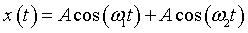
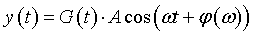
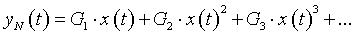
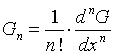
[43]  J. C. Pedro and N. B. Carvalho. 2003, “Intermodulation Distortion in Microwave and Wireless Circuits,” Artech House, London.