-
Paper Information
- Next Paper
- Previous Paper
- Paper Submission
-
Journal Information
- About This Journal
- Editorial Board
- Current Issue
- Archive
- Author Guidelines
- Contact Us
Electrical and Electronic Engineering
p-ISSN: 2162-9455 e-ISSN: 2162-8459
2012; 2(6): 397-402
doi: 10.5923/j.eee.20120206.09
Gate Leakage Current in GaN HEMT’s: A Degradation Modeling Approach
 Abstract
 Reference
 Full-Text PDF
 Full-Text HTML
A. Mimouni1, T. Fernández1, J. Rodriguez-Tellez1, A. Tazon1, H. Baudrand2, M. Boussuis3
1Departamento de Ingeniería de Comunicaciones-Universidad de Cantabria Laboratorios I+D+i de Telecomunicaciones, Santander, 39005, Spain
2Henri Baudrand Laboratoire LAPLACE-GRE ENSEEIHT 2, BP 7122, 31071 Toulouse CEDEX 7, France
3Département de Physique, Université Abdelmalek Essaâdi, Faculté des sciences Tétouan, 93030, Maroc
Correspondence to: A. Mimouni, Departamento de Ingeniería de Comunicaciones-Universidad de Cantabria Laboratorios I+D+i de Telecomunicaciones, Santander, 39005, Spain.
| Email: |  |
Copyright © 2012 Scientific & Academic Publishing. All Rights Reserved.
In this paper we present an empirical preliminary model able to simulate the degradation with time in the gate leakage current in GaN HEMT devices. The model is based on extensive reverse and forward current measurements, carried out on a wide range of different device designs and under different bias, performed over aged transistors by III-V Lab (Alcatel-Thales) within the European KORRIGAN. A closed form expression for the reverse gate current, depending on time, as well as the expression parameters extraction procedure are presented. The experimental and simulated results presented illustrate the validity of the model as well as it’s usefulness in reliability studies.
Keywords: Leakage Current, GaN HEMT, Modeling
Cite this paper: A. Mimouni, T. Fernández, J. Rodriguez-Tellez, A. Tazon, H. Baudrand, M. Boussuis, "Gate Leakage Current in GaN HEMT’s: A Degradation Modeling Approach", Electrical and Electronic Engineering, Vol. 2 No. 6, 2012, pp. 397-402. doi: 10.5923/j.eee.20120206.09.
Article Outline
1. Introduction
- In applications such as high-power and high-frequency amplifiers for base stations AlGaN/GaN HEMT devices offer the circuit designer certain advantages over the more traditional GaAs devices. These mostly relate to the ability of these devices to handle high operating voltages under high current conditions. Their main drawback, however, relates to their reliability which needs to improve considerably[1]. While reliability issues have been considered by others on AlGaN/GaN devices[2-5] the emphasis of the work has been on the degradation in the output current, the power dissipated and the drain resistance Rd of such devices[6]. The degradation effects on the gate leakage current arises as an important feature when studying GaN HEMT reliability[7-12], being worthy of note its effect on the saturation current and breakdown voltage parameters of the device[13].In this paper we present an empirical model able to simulate the degradation in the gate leakage current with time on AlGaN/GaN devices. The model presented in this work is based on extensive experimental measurements carried out by III-V Lab (Alcatel-Thales) within the European KORRIGAN project on many specimens over prolonged periods of time (2000 hours).
2. Gate Leakage Current
- As stated previously, AlGaN/GaN HEMT devices are well suited to high-power high-frequency applications such as high power amplifiers and applications for wireless base stations. For such cases there is a general requirement for a low input gate current and a high reliability figure for the device. In previously reported work[14] the role played by the degradation with time in the gate leakage current is important in the understanding of the reliability issue for the device.From a physical point of view the degradation, and hence changes observed with the device, arise from defects under the gate region. These become more evident at a critical point in the value of the electric field[13-14]. Trap formation in the device at either the semiconductor surface or within the bulk is also a performance-limiting issue. To date, however, a clear explanation for the physical mechanisms which ties together the failure or reliability of the device and the degradation in it’s electrical characteristics is unavailable. The gate leakage current surges as a consequence of surface processing and passivation issues. In Field Effect devices quantum mechanical tunnelling has been clearly shown to be an important effect to be accounted for[13]. For example, electrons tunnelling from the gate can create a gate-to-drain leakage current by hopping from trap to trap. Alternatively, the electrons can accumulate on the surface next to the gate or move through the AlGaN layer to the conducting channel[15].A model to simulate the gate leakage current in GaAs MESFET’s due to tunnelling effects is described in[16]. This model was subsequently altered in[17] to be applicable to GaN devices.The gate leakage current due to tunnelling effects is represented in circuit form as a generator connected between the gate and drain terminals of the device. The electric field at the edge of the gate terminal is reduced by the electrostatic feedback. This reduces the electron tunnel leakage current. As the number of electrons increases at the gate edge as a function of time the gate leakage current reduces due to the feedback. In addition, the increased electron density on the AlGaN surface decreases the number of 2DEG electrons and this causes the gate current to decrease[15-16].
3. Gate Leakage Current Degradation Model
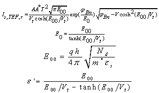
- The leakage mechanism in GaN and AlGaN Schottky interfaces was considered by Yu et al[18] and Miller et al[19]. This work was based on field-emission tunnelling transport assuming a triangular Schottky potential distribution. To obtain good agreement with experimental results, however, requires a value for the donor density which is higher than in practice. This led them to suggest a defect-assisted tunnelling mechanism to increase the leakage current.A surface patch model was proposed by Sawada et al[20] to explain the forward current characteristics. Miller et al[21] have also proposed a leakage mechanism associated with a variable- range hopping conduction through threading dislocations. As will be demonstrated later, we have found the thermionic field emission (TFE) model to provide a good compromise between accuracy and ease of parameter extraction.In the TFE model, the reverse current, Igleak, arises from electrons that are thermally excited from the metal Fermi junction and tunnel through the semiconductor depletion layer to the semiconductor conduction band[22].The reverse current can be expressed by the following equations[22]:
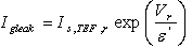 | (1) |
 | (2) |
 is the Schottky barrier height. The term
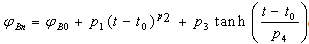
  is the characteristic energy related to the tunneling probability in the Wentzel–Kramers– Brillouin approximation which depends on the donor density Nd.From the life tests (electrical and thermal aging for a total duration in the region of 2000 hours) experimental results, we observe that the most time dependent parameters were the Schottky barrier height and the donor density Nd[18- 19]. From reverse and forward current measurements (carried out on a wide range of different device designs and under different bias) performed over aged devices, we have observed that the time dependency of parameters Nd and
  can be expressed, from a macroscopic point of view, as:
 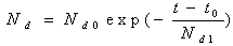 | (3) |
 | (4) |
4. Results and Discussion
4.1. Device description and Performed Measurements
- In order to validate the approach adopted, five aged devices (two with a gate-width of 2X75
 and three with a gate-width of 8X75
 provided by III-V Lab (Alcatel-Thales) are employed. For these devices, forward and reverse gate current measurements are performed at our laboratories.The 8x75
 devices, are fabricated using an undoped multilayer structure consisting of a GaN buffer layer (1.5
 ), followed by an AlGaN barrier layer (22.0 nm thickness, 27% Al concentration). These GaN HEMTs are fabricated on all wafers using the same industrial quality process, including ohmic contact formation through Ti/Al/Ni/Au deposition and Schottky gate electrode formation using Mo/Au deposition. In the case of the 2x75
 devices, the undoped multilayer structure consisted of a GaN buffer layer (1.0
 ), followed by an AlGaN barrier layer (27.5 nm thickness, 30.3% Al concentration). These GaN HEMTs are fabricated on all wafers using the same industrial quality process, including ohmic contact formation through Ti/Al/Pt/Au deposition and Schottky gate electrode formation using Ni/Au deposition.During the aging test, several DC life tests are launched in order to evaluate the effect of the temperature junction on the degradation of the transistors. The different ambient temperatures of the junction are selected at 150℃, 175℃, 250°C and 300°C. The tests duration are targeted at 1000 or 2000 hours.The bias point used in the aging test is 25V Vds and Ids 420 mA/mm. The drain current is kept constant by automatic gate voltage control so that the dissipated power is constant and the temperature of the junction as well. In Table 1, summarizes the test conditions for the different devices during the aging process
 device. The measurements were performed as a function of Vgs at a Vds of 25V after thermal and electrical aging at the temperature T = 175℃.
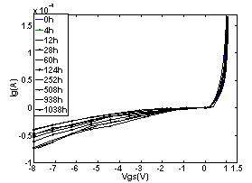 | Figure 1. Measured gate current versus gate-source voltage as a function of aging time (hours) at Vds=25V for device D5 |
4.2. Extraction of the Model Parameters
- In brief, the extraction of the model parameters is performed in three steps as:(i). At time t0, the value of parameter
 is obtained using a high precision current source. For this measurement the gate-drain junction is forward biased Figure 2 and the parameter measured under very low current conditions (<1mA) so that the parasitic resistance of the device has a negligible effect. Clearly this assumption is only valid under this condition and for the purpose of extracting this parameter. (ii). The device is then aged over time according to the conditions shown in Table 1. For each device and test condition, measurements are made under forward (step (i)) and reverse bias conditions as shown in Figure 1. For each device, parameters Nd0 (at time t = 0 h) and Nd1 are determined from reverse bias measurements. Using this information parameter Nd is then calculated and optimised. (iii). The parameters (p1, p2, p3 and p4) of equation (4) are obtained from forward bias measurements (Figure 2). Prior to extracting these parameters the measured current values are adjusted using the parameter values of equation (4) determined previously.
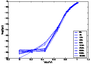 | Figure 2. Forward bias measurements gate current versus gate-source voltage as a function of aging time for device D5 |
|
|
 device the value of parameter
 reduces as the ambient temperature increases. This is also in keeping with the results presented elsewhere[24, 25]. This can be explained by the fact that the additional ionized doping atoms, arising from the positive fixed charge at the surface, increases the number of ionized doping atoms at the surface. Tunnelling is, therefore, easier since the barrier is thinner at the surface.The devices studied in this work are different transistors gallium nitride HEMT of Waffer (AEC1303) and Waffer (AEC1388) submitted to different thermal and electrical aging , as shown in the table 1; this can explain the observed differences between the value of the parameters of equation 7 for the devices studied. As an example, the value of parameter p1 for the device D1 and D5 is negative while for the other devices is positive; and that can be explained by: the measurement results Ig with time decreases and also the first part of the equation 4 is a polynomial. Figures 3 and 4 Show the evolution of with time for devices under test.
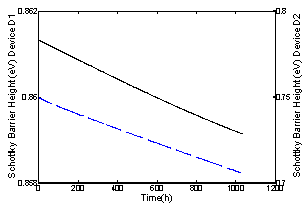 | Figure 3. Time-dependent for D1 (solid) and D2 (dotted) devices |
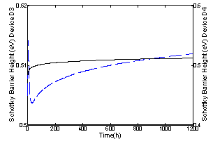 | Figure 4. Time-dependent for D3 (solid) and D4 (dotted) devices |
 and 2X75
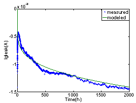
 devices using the conditions shown in Table 1. The results indicate good agreement between the experimental and modelling approach. The discrepancies between the measured and simulated results are largely due to measurement errors and the optimisation strategy employed to refine the model parameter values. These two areas are under consideration taking into account the need for the model and general approach to be useful to devices fabricated by a wide range of foundry houses and processing conditions.
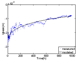
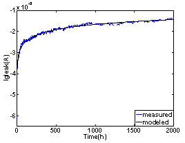
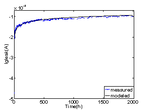
 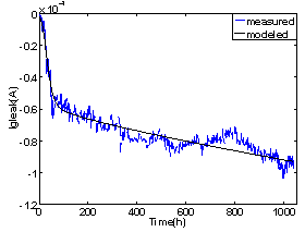 | Figure 5. Modelled and measured stress time-dependent Igleak for D1 device |
 | Figure 6. Modelled and measured stress time-dependent Igleak for D2 device |
 | Figure 7. Modelled and measured stress time-dependent Igleak for D3 device |
 | Figure 8. Modelled and measured stress time-dependent Igleak for D4 device |
 | Figure 9. Modelled and measured stress time-dependent Igleak for D5 device |
5. Conclusions
- A model to simulate the degradation in the leakage current with time has been applied to AlGaN/GaN HEMT devices of varying sizes from different manufacturers. These have been measured under a variety of test conditions including various ambient temperature points. The results clearly show a strong dependence between the leakage current, the barrier potential and the donor density of the gate-drain junction. These results also demonstrate the strong influence that the surface and bulk traps of the material have on the leakage current. Not unexpectedly the results also demonstrate the strong inter-dependence between these variables and the ambient temperature.
ACKNOWLEDGEMENTS
- This work was supported in part by the Spanish Ministry of Education and Science through theTEC2008-06684-C03-01 project and by CIDA (Spanish Armada) under KORRIGAN contract EDA (RTP102.052).
References
| [1] | C. Lee, L. Witkowski, H.-Q. Tserng, P. Saunier, R. Birkhahn, Dan Olson, G. Munns, S. Guo, B. Albert, “Effects of AlGaN/GaN HEMT structure on RF reliability”, Electron. Lett., vol. 41 no. 3, pp. 155-157, Feb. 2005. |
| [2] | K.S. Boutros, P. Rowell, and B. Brar, “A study of output power stability of GaN HEMTs on SiC substrates”, in Proc. of the IEEE Int. Rel. Phys. Symp. (IRPS), pp. 577-578, 2004. |
| [3] | N. Malbert, N. Labat, A. Curutchet, C. Sury, V. Hoel, J.-C. de Jaeger, N. Defrance, Y. Douvry, C. Dua, M. Oualli, C. Bru-Chevallier, J.-M. Bluet, W. Chikhaoui “Characterisation and modelling of parasitic effects and failure mechanisms in AlGaN/GaN HEMTs” Microelectronics Reliability, 49, pp. 1216-1221, 2009. |
| [4] | J. W. Chung, J. C. Roberts, E. L. Piner, and T. Palacios, “Effect of gate leakage in the subthreshold characteristics of AlGaN/GaN HEMTs,” IEEE Electron Device Lett., vol. 29, no. 11, pp. 1196–1198, Nov. 2008. |
| [5] | G. Meneghesso, G. Verzellesi, F. Danesin, F. Rampazzo, F. Zanon, A. Tazzoli, M. Meneghini, E. Zanoni”, Reliability of GaNhigh-electron-mobility transistors: state of the art and perspectives”, IEEE Trans Dev Mater Reliab, 8 (2008), pp. 332–343. |
| [6] | Ho Jun Nam, Hong Goo Choi, Min-Woo Ha, Hong Joo Song, Cheong Hyun Roh, Jun Ho Lee and Cheol-Koo Hahn, “Suppression of Leakage Currents in AlGaN/GaN HEMTs by Optimizing the Thermal Ramping Rate during the Ohmic RTP Process”, Journal of the Korean Physical Society, Vol. 59, No. 2, pp. 439-442, August 2011. |
| [7] | Yu-Syuan Lin, Yi-Wei Lain, and Shawn S. H. Hsu, “AlGaN/GaN HEMTs With Low Leakage Current and High On/Off Current Ratio”, IEEE ELECTRON DEVICE LETTERS, VOL. 31, NO. 2, FEBRUARY 2010. |
| [8] | J. W. Chung, J. C. Roberts, E. L. Piner, and T. Palacios, “Effect of gate leakage in the subthreshold characteristics of AlGaN/GaN HEMTs,” IEEE Electron Device Lett., vol. 29, no. 11, pp. 1196–1198, Nov. 2008. |
| [9] | G. Meneghesso, G. Verzellesi, F. Danesin, F. Rampazzo, F. Zanon,A. Tazzoli, M. Meneghini, and E. Zanoni, “Reliability of GaN high electron-mobility transistors: State of the art and perspectives,” IEEE Trans. Device Mater. Rel., vol. 8, no. 2, pp. 332–343, Jun. 2008. |
| [10] | E. Zanoni, and all. “Localized Damage in AlGaN/GaN HEMTs Induced by Reverse-Bias Testing”, IEEE ELECTRON DEVICE LETTERS, VOL. 30, NO. 5, MAY 2009. |
| [11] | M. Meneghini, A. Stocco, M. Bertin, C. de Santi, F. Rampazzo, D. Marcon, G. Meneghesso, E. Zanoni, “Degradation of AlGaN/GaN HEMTs below the “critical voltage”: a time-dependent analysis”, CS MANTECH Conference, April 23rd - 26th, 2012, Boston, Massachusetts, USA. |
| [12] | Z. H. Liu, G. I. Ng, H. Zhou, S. Arulkumaran, and Y. K. T. Maung, “Reduced surface leakage current and trapping effects in AlGaN/GaN high electron mobility transistors on silicon with SiN/Al2O3 passivation”, Appl. Phys. Lett. 98, 113506, 2011. |
| [13] | Jungwoo Joh and Jesús A. del Alamo, “Mechanisms for Electrical Degradation of GaN High-Electron Mobility Transistors”, Electron Devices Meeting, 2006. IEDM ’06, International, pp. 1-4, Dec. 2006 |
| [14] | Y. Inoue and all., “Degradation-mode analysis for highly reliable GaN HEMT”, IEEE IMS Technical Digest, pp. 639-642, June 2007. |
| [15] | R. J. Trew, Y. Liu, W. W. Kuang, and G. L. Bilbro, “The physics of reliability for high voltage AlGaN/GaN HFET’s,” in IEEE CSICS Symp. Dig., San Antonio, TX, pp. 103-106, 2006. |
| [16] | Robert J. Trew, Daniel S. Green, and Jeffery B. Schealy, “AlGaN/GaN HFET Reliability,” IEEE microwave magazine, pp. 116-127, Jun. 2009 |
| [17] | Q.Z.LIU and S.S. LAU, “A Reviews Of The Metal-GaN Contact Technology,” Solid-State Electronics Vol.42, Nº.5, pp. 677-691, 1998. |
| [18] | L. S. Yu, Q. Z. Liu, Q. J. Xing, D. J. Qiao, and S. S. Lau and J. Redwing, “The role of the tunneling component in the current–voltage characteristics of metal-GaN Schottky diodes”, J. Appl. Phys. 84, pp. 71-76, 1998. |
| [19] | E. J. Miller, X. Z. Dang and E. T. Yu, “gate leakage current mechanisms in AlGaN/GaN heterostructure field-effect transistors”, J. Appl. Phys. 88, pp. 5951-5998, 2000. |
| [20] | T. Sawada, Y. Ito, K. Imai, K. Suzuki, H. Tomozawa and S. Sakai, “Electrical properties of metal/GaN and SiO2/GaN interfaces and effects of thermal annealing”,Appl. Surf. Sci. 159-160 (2000) 449-455. |
| [21] | E. J. Miller, E. T. Yu, P. Waltereit and J. S. Speck, “Analysis of reverse-bias leakage current mechanisms in GaN grown by molecular-beam epitaxy”, Appl. Phys. Lett. 84, Nº4, pp. 535-537, 2004. |
| [22] | Padavoni FA, “Stratton R. Field and thermionic-field emission in Schottky barriers”, Solid –State Electron, pp. 9-695, 1966. |
| [23] | E.A.Douglas, C.Y. Chang and all, “AlGaN/GaN Electron mobility transistor degradation under on- and off-state stress” Microelectronics Realiability (2010). |
| [24] | Q.Z.LIU and S.S. LAU, “A Reviews Of The Metal-GaN Contact Technology,” Solid-State Electronics Vol.42, Nº.5, pp. 677-691, 1998.Applications Symposium, Bologna, Italy – September 3rd-5th, 1997. |
| [25] | J. Osvald , J. Kuzmik and all, “ Temperature dependence of GaN Schottky diodes I/V characteristics”, Microelectronic Engineering 81, pp. 181-187, 2005. |
| [26] | J. Kotani and all, “Tunneling Injection of Electrons at Nanometer-Scale Schottky Gate Edge of AlGaN/GaN Heterostructure Transistors and Its Computer Simulation”, e-J. Surf. Sci. Nanotech. Vol. 3, pp. 433-438, 2005. |