Santanu Sharma , Kabita Chaudhury
Department of ECE, Tezpur University Napaam, Assam, India
Correspondence to: Santanu Sharma , Department of ECE, Tezpur University Napaam, Assam, India.
| Email: |  |
Copyright © 2012 Scientific & Academic Publishing. All Rights Reserved.
Abstract
Square gate all around MOSFET is a promising device structure at present era of continued scaling due to their superior control over the short channel effects. However, it exhibits a undesirable effect known as corner effect which degrades the device performance by increasing the off state leakage current. In this work a new technique to suppress the corner effect has been proposed, modelled, simulated and its results have been compared with existing structure of square gate all around MOSFET.
Keywords:
Square Gate All Around MOSFET, Corner Effect, charge sharing, premature inversion
Cite this paper:
Santanu Sharma , Kabita Chaudhury , "A Novel Technique for Suppression of Corner Effect in Square Gate All Around Mosfet", Electrical and Electronic Engineering, Vol. 2 No. 5, 2012, pp. 336-341. doi: 10.5923/j.eee.20120205.14.
1. Introduction
The scaling of classical MOSFET is approaching its limit due to the short channel effects. So to overcome this problem multiple gate MOSFETs were introduced as a replacement of classical single gate MOSFET. As the numbers of gate increases multiple gate MOSFETs offer superior control over the channel, which helps to reduce short channel effects and leakage current[1]-[4]. According to the numbers of gates multiple gate MOSFETs are of various types, like Double gate MOSFET, Tri gate MOSFET, Gate all around(GAA) MOSFET (Cylindrical and Square). Among these multiple gate structures, Gate all around structure offers superior control over the channel due to its surrounding gate structure, which in turn reduces the short channel effect effectively[5]-[6]. Besides, GAA MOSFETs offer several advantages over single and other multiple gate MOSFETs like higher current drivability, mobility enhancement and so on. So due to these advantages, gate all around MOSFETs are considered as the excellent candidates for future CMOS integration.Among the Gate all around structures, square gate all around MOSFET has higher current drive capability compared to cylindrical gate all around MOSFET. Despite these advantages, square gate all around MOSFET exhibits a very undesirable characteristic known as corner effect which occurs due to the electrostatic coupling of two adjacent gates at the corners. This effect degrades the device performance by increasing the off state leakage current. The corner effect can be minimized by rounding the corner regions [7]. But corner rounding is a delicate process. In this paper we propose a new method to suppress the corner effect occurs in square gate all around MOSFET.Section 2 of the paper describes the corner effect of square gate all around MOSFET. Section 3 describes the newly proposed method for suppression of corner effect. The results of this newly proposed method has been discussed in section 4. Finally the section 5 carries the conclusion of this paper.
2. Corner Effect in Square GAA Mosfets
Square gate all around MOSFET is types of multigate MOSFET where the gate warps around the four sides of the silicon channel[8]. The square gate all around MOSFET and its schematic description is shown in figure 1. The cross-section of the silicon surface has a square shape with width and height tsi. A layer of silicon dioxide (SiO2) having thickness tOX, is warped around the silicon surface which acts as an insulator between silicon surface and gate electrode. Since the gate electrode has wrapped the device in all directions, so at the corner regions as shown in figure 2 of the device due to the electrostatic coupling of two adjacent gates, charge sharing effect occurs that means at the corner region, the depletion charge is shared by two gates[9]. This causes reduction of threshold voltage at the corners. So the corners are turned on prior to the other parts of the device. So, premature inversions occur at the corners. This phenomenon is known as corner effect [10]-[11]. The threshold voltage of a square gate all around MOSFET is as follows | (1) |
Since depletion charge has been shared by two adjacent gates at the corners so at the corner regions depletion regions charge density reaches maximum value, when the gate contributes only half in the other parts. This causes reduction of surface potential. Mathematically it can be presented as,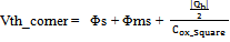 | (2) |
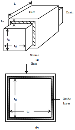 | Figure 1. (a) Square gate all around MOSFET (b) Cross-section of square gate all around MOSFET |
For square GAA MOSFET oxide capacitance is given by [12]
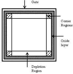 | Figure 2. Square gate all around MOSFET with corner regions |
At corner region charge contributed by each gate is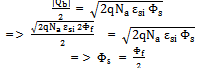 | (3) |
So at the corner region threshold voltage is reduced to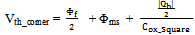 | (4) |
Figure 3 shows the variation of threshold voltage at the corners and other parts of a square gate all around MOSFET using n+ polysilicon gate.This results increase of drain current at the corners. This corner current for linear region can be modelled as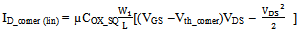 | (5) |
 | (6) |
For saturation region | (7) |
And current at other parts of the channel isFor linear region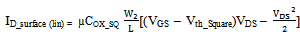 | (8) |
For saturation region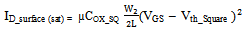 | (9) |
 | (10) |
So the total drain current of a square gate all around MOSFET for linear region | (11) |
For saturation region | (12) |
Figure 4 shows the variation of current at corners and other parts of the channel. Since current at the corners more than other parts of the channel so it degrades device performance. 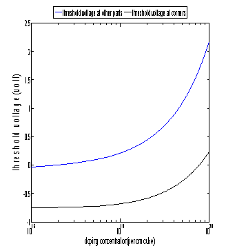 | Figure 3. Variation of threshold voltage at corners and other parts of the device |
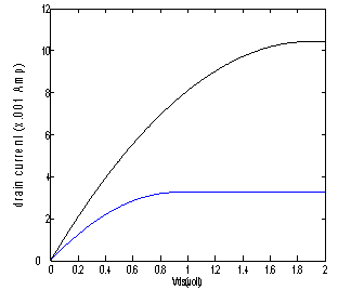 | Figure 4. Variation of drain current at corners and other parts of the channel |
3. A Novel Technique for Suppression of Corner Effect
The main reason behind the corner effect is charge sharing at corners. To overcome this problem in this work a new structure of square gate all around MOSFET has been proposed. This is known as “ Square gate all around MOSFET with lateral gate underlap”. In this structure instead of applying the gate in all directions, four gates are given to the four sides of the device with reduced gate width i.e the width is reduced from both the ends of the gate in each four sides of the device. Figure 5 shows the structure of a square gate all around MOSFET with lateral gate underlap. The width of the each gate is W and the thickness of the silicon surface is tsi. The width of the underlap region on both ends of each gate is .This structure can be better explained with the aid of a parallel plate capacitor with unequal plate area. Suppose the gate material is considered as the upper plate and silicon surface is lower plate. Length of the upper plate is L and its width is W, while the width of the lower plate is W+2w’ as shown in figure 6. Distance between two plates is tOX and permittivity is εOX. So the capacitance at the region where both plates are of equal dimensions is
 | (13) |
For unequal plate region there exists an additional width at the lower plate w’ on each side. The electric field (E) of the equal plate portion is uniform. But in unequal plate portion it is not uniform. In both sides of the additional width, as the width increases the electric field decreases as Ecosθ1, Ecosθ2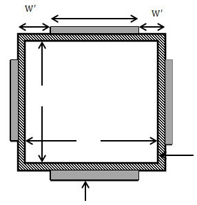 | Figure 5. Square gate all around MOSFET with gate underlap |
 | Figure 6. Parallel plate capacitor with unequal plate dimension |
and so on and so as capacitance. This variation of electric field is shown in figure 7. So the total electric field in unequal plate portion is  | (14) |
Now, total capacitance of the unequal plate portion is | (15) |
According to Gauss law,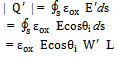 | (16) |
So, | (17) |
Now for per unit area of the unequal parallel plate section capacitance is | (18) |
Where θi is the maximum range up to which electric field can generate in unequal parallel plate section of the MOS and it can calculate as  | (19) |
 | Figure 7. Variation of electric field in unequal parallel plate portion |
The capacitance of the unequal parallel plate section of the device is less than the capacitance of the equal parallel plate. To minimize the corner effect up to highest possible level, the capacitance of unequal parallel plate section is considered as half of the capacitance of the equal parallel plate portion. Mathematically, | (20) |
 | (21) |
So to minimize corner effect, underlaped region should be 1.73 times of the oxide thickness. Which means that the amount of width which is removed from both the ends of all four gates in four sides of the device is equal to 1.73 times of tOX.Since width of all the four gates are reduced, so when a positive voltage is applied to all four gates a depletion region will create at the beneath of each gate. But due to the fringing electric field, a smaller depletion region will generate in gate underlap region. So the depletion charge of this depletion region is less than the depletion region generated beneath the gate. Here it is assumed that the depletion charge of gate underlap region is the half of the depletion charge of actual depletion region. So, | (22) |
Since the it is contributed by both the sides, so overall charge density becomes Qb only.The threshold voltage at the non underlap gate region is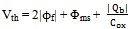 | (23) |
Where, 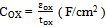 In case of square gate all around MOSFET with gate underlap structure, at the underlap region capacitance and depletion charge is reduced to half of the capacitance and depletion charge of non underlap region. The threshold voltage at the unerlap region is
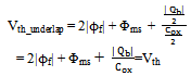 | (24) |
So threshold voltage at gate underlap region is same as non underlap region. So in square gate all around MOSFET with gate underlap structure, threshold voltage at corner region remain same as the threshold voltage at other parts of the device. This results in corner current and total current of the device. The modified corner current is For linear region | (25) |
For saturation region 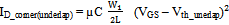 | (26) |
C = capacitance at gate underlap regions From equation 20  And from equation 24
 So the equation 25 can be written asFor linear region
 | (27) |
For saturation region  | (28) |
The total current of the device at linear region  | (29) |
 | (30) |
And for saturation regions | (31) |
So from equation 30 and 31 it is clear that the corner current of a square gate all around MOSFET with gate underlap structure is lower than the corner current of a normal square gate MOSFET. So using gate underlap technique corner current can be minimized. But simultaneously it reduces the total current driving capability of the device.
4. Results and Discussion
To minimize the corner effect a new structure of square gate all around gate MOSFET has been discussed in section 3. In this structure four gates are given to the four sides of the device with reduced gate width. The physics of this new structure is similar to a parallel plate capacitor with unequal plate dimensions. In parallel plate capacitor the capacitance is uniform at the region where both plates are of equal dimensions due. But electric field is not uniform in the region where both the plates are of not equal dimensions. In this region electric field is reduced which in turn reduces the capacitance. Figure 8 shows the plot of variation of capacitance in gate underlap region. The capacitance decreases in gate underlap region and it becomes half at the corner position. 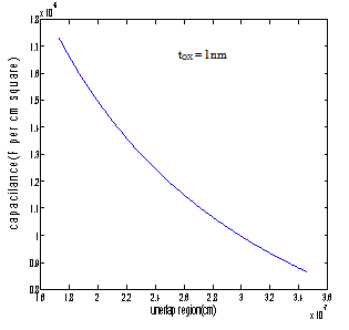 | Figure 8. Variation of capacitance at gate underlap region |
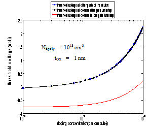 | Figure 9. Variation of threshold voltage at corner positions and other parts of the device with and without using gate underlap technique |
Figure 9 shows the variation of threshold voltage with doping concentration at corner regions and the other parts of the device for a square gate all around MOSFET with and without gate underlap. It is clearly shown that for a square gate all around MOSFET without gate underalp the threshold voltage at the corner regions is lower than the other parts. But for a square gate all around MOSFET with gate underlap, threshold voltage is equal at corner positions and other parts which can be seen from figure 9. 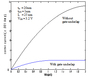 | Figure 10. Reduction of corner current with gate underlap |
 | Figure 11. Reduction of total current with gate underlap |
 | Figure 12. Reuduction of subthreshold leakage current with gate underlap |
Figure 10 shows corner current- Vds plot for a square gate all around MOSFET with and without gate underlap. Since for a gate underlap structure threshold voltage is equal at corner positions and other parts, so current at corner regions remain same as other parts of the device. So using gate underlap structure corner current can be minimized, which is clearly shown in figure 10.Figure 11 shows total current- Vds plot for a square gate all around MOSFET with and without using gate unerlap. Since corner current is reduced using gate underlap (from figure 10), hence it reduces the total current of the device.Figure 12 shows the variation of subthreshold leakage current for a square gate all around MOSFET with and without using gate underlap. From this figure it can be observed that subthreshold leakage current is lower in case of gate underlap structure.
5. Conclusions
This paper studies the corner effect of a square gate all around MOSFET which occurs due to charge sharing effect between two adjacent gates. This effect degrades the device performance by increasing the current at corners leading to premature inversion. To minimize this effect, in this paper a new structure of square gate all around MOSFET known as “square gate all around MOSFET with gate underlap” has been proposed and the same has been modeled and simulated. Also this model has been compared with conventional square gate all around MOSFET. From this comparison it is clear that the threshold voltage and hence the current at the corner regions of this new structure is same as the threshold voltage and current at other parts of the device. It also reduces the subthreshold leakage current. But simultaneously this structure reduces the total current of the device. Although this structure reduces the total current driving capability of the device still it protects the device from unwanted corner effect.
References
| [1] | I. Ferain, C. A. Colinge & J. -P. Colinge, “ Multigate transistors as the future of classicalmetal–oxide–semiconductor field-effect transistors”, NATURE, vol. 479, pp. 310-317, Nov. 2011. |
| [2] | J. P. Colinge, “The New Generation of SOI MOSFET”, RomanianJournal of Information Science and Technology, vol. 11, pp. 3-15, 2008. |
| [3] | T. Poiroux, M. Vinet, O. Faynot, J. Widiez, J. Lolivier, T. Ernst, B. Previtali, S. Deleonibus, “Multiple Gate Devices: Advantages and Challenges”, Microelectronic Engineering, vol. 80, pp. 378–385, 2005. |
| [4] | A. Das Gupta, “Multiple Gate MOSFETs:The Road to the Future”, Physics of Semiconductor Devices, pp. 96-101, 2007. |
| [5] | D. Jiménez, J. J. Sáenz, B. Iñíguez, J. Suñé, L. F. Marsal and J. Pallarès, “Modeling of Nanoscale Gate-All-Around MOSFETs”, IEEE Electron Device Letters, vol. 25, no. 5, May 2004. |
| [6] | J.-T. Park and J.-P. Colinge, “Multiple-gate SOI MOSFETs: Device design guidelines,” IEEE Trans. Electron Devices, vol. 49, no. 12, pp. 2222–2229, December 2002. |
| [7] | Chi-Woo Lee, Se-Re-Na Yun, Chong-Gun Yu, Jong-Tae Park, Jean-Pierre Colinge, “Device design guidelines for nano-scale MuGFETs” Solid State Electronics, vol. 51, pp. 505- 510, 2007. |
| [8] | S. K. Vishvakarma, U. Monga, T. A.Fjeldly, “Analytical Modeling of the Subthreshold Electrostatics of Nanoscale GAA Square Gate MOSFETs”, NSTI-Nanotech, vol. 2, pp. 789-792, 2010. |
| [9] | J. -P. Colinge,FinFET and Other Multi-Gate Transistors, Springer 2008. |
| [10] | M. P. Kumar, S. K. Gupta and M. Paul, “Corner Effects in SOI-Tri gate FinFET structure by using 3D Process and Device Simulations”, 3rd IEEE International Conference on Computer Science and Information Technology (ICCSIT), vol. 9, pp. 704 – 707, 2010. |
| [11] | W. Xiong, J. W. Park, and J. P. Colinge, “Corner effect in multiple-gate SOI MOSEFT”, IEEE International SOI Conference, pp. 111–113, 2003. |
| [12] | I.M. Tienda-Luna, F.J. García Ruiz, L. Donetti, A. Godoy and F. Gámiz, “Modeling the equivalent oxide thickness of Surrounding Gate SOI devices with high-κ insulators”, Solid- State Electronics, vol. 52, pp. 1854-1860, 2008. |
 Abstract
 Reference
 Full-Text PDF
 Full-Text HTML