Jae-Hyok Ko , Kwan-Young Kim , Han-Gu Kim
System LSI Business Department, Samsung Electronics Co., Ltd., Yongin-City, 449-711, Korea
Correspondence to: Jae-Hyok Ko , System LSI Business Department, Samsung Electronics Co., Ltd., Yongin-City, 449-711, Korea.
| Email: |  |
Copyright © 2012 Scientific & Academic Publishing. All Rights Reserved.
Abstract
System level ESD protection methodology for mobile display driver IC is discussed at the viewpoint of hard and soft failure caused by injected ESD charge into I/O pins from LCD panel. The key design factor was analysed through device simulation, successfully implemented to IC and verified at system level ESD evaluation.
Keywords:
System-Level ESD, Hard Failure, Soft Failure, Driver IC ESD
Cite this paper:
Jae-Hyok Ko , Kwan-Young Kim , Han-Gu Kim , "System-Level ESD Immunity of Mobile Display Driver IC to Hard and Soft Failure", Electrical and Electronic Engineering, Vol. 2 No. 5, 2012, pp. 329-335. doi: 10.5923/j.eee.20120205.13.
1. Introduction
Nowadays, system level ESD (Electrostatic Discharge) on-chip protection for display driver IC has been being strongly emphasized because module makers continue to strive to save cost on fixing module design to meet the system level ESD specifications. These attempts make IC ESD designers look into not only component but also system level ESD protection methodology. Among the various components of mobile LCD (Liquid Crystal Display) module, display driver IC is prone to be the most threatened by ESD charge injected from LCD panel because it is an unique component directly connected to ESD zapped panel and made up of very-large-scale- integrated devices which are thermally weak in comparison with the discrete devices such as capacitor, resistor or diode existing outside of driver IC for the purpose of LCD regular operation. This thermal weakness for driver IC frequently provides a reason for the on-chip hard failure by system level ESD stress. Moreover, storage elements such as graphic memory bit and latch cell within logic P&R block can easily lose their data due to the power upset during system level ESD event. It leads to the soft failure which can be recovered by hardware reset of power on-off or software reset operation.In this paper, case study for hard failure caused by system level ESD test for mobile LCD module is first introduced to explain the discharge mechanism by the well-to-well charge coupling between independent powers not connected by intended ESD protection devices or the circuitries. This in-depth analysis for hard failure includes the waveform measurement for the coupled potential, physical damage analysis and its failure modelling. Mobile LCD driver IC has row/column line drivers and the row line driver needs both positive and negative biases for panel TFT (thin film transistor) on-off. So, a triple well structure in process architecture respect is essential to isolate between ground and negative bias in the mobile display driver IC. Analysis results in this paper show that a triple well structure easily provides an opportunity for charge coupling between neighbouring NWELLs (N-type diffused wells) during system level ESD event.Case study for soft failure[1-8] during system level ESD event for mobile LCD module is presented through failure analysis and its modelling result. The analysis results show the similar discharge mechanism to that of the hard failure, which was disturbed by system level ESD stress. NWELL within ESD protection cell for critical I/O pin, which is heavily exposed to ESD charge injected from LCD panel, can facilitate exciting its adjoining NWELL during ESD event. So, the bias of the adjoining NWELL can be fluctuated due to the well-to-well charge coupling through a turn-on action of the parasitic NPN bipolar which is made by NWELLs and PWELL (P-type diffused well) between the two, even though one of the two NWELLs has no relation with the ESD source. This coupling mechanism can explain the data loss of local memory bits during ESD event and lead to the soft failure of display driver IC.Through the two case studies of hard and soft failures by system level ESD test, we have known that the triple well structure in the mobile display driver IC can put it at a disadvantage in protecting core circuit from being contaminated by injected charge through the well-to-well charge coupling. ESD design concept of so called ‘NWELL catch-up guard ring’ that is inserted between adjoining NWELLs with its bias grounded is introduced to alleviate the coupling effect from the well-to-well NPN bipolar turn-on. In order to investigate the diffusion depth effect of the suggested NWELL catch-up guard ring on the potential clamping ability during system level ESD event, TCAD simulation has been carried out and the results explain that the NWELL diffusion depth in catch-up guard ring is a critical factor which can be in control of the node potential clamping level. Mobile display driver IC with the proposed catch-up guard ring scheme was successfully implemented in 0.09μm/30V HV CMOS technology and showed that IC with poor level of soft failure by the system level ESD stress was dramatically improved.
2. Failure Analysis (Hard Failure)
System level ESD test has been performed for the mobile LCD module with QVGA (Quarter Video Array, 320X240) resolution which is attached to test board by display module connector. Gun with the 330Ω/150pF R-C module is discharged by 8kV air mode following IEC-61000-4-2 standard[9] toward the various discharge areas in panel center and corner. Figure 1 shows the display images before and after zapping ESD for the LCD module.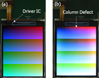 | Figure 1. Display images before and after ESD stress (a) before ESD zapping (b) after ESD zapping (column line defect) |
Figure 1 (a) and (b) exhibit that column line defects after ESD stress occurred in the vicinity of panel center. This display failure is accompanied by over-current of additional IDD 1mA to the normal IDD and of course, it can be not recovered. Commonly, mobile display driver IC supporting a-Si TFT contains a large number of gate and source drivers in order to display image on the panel. Source driver plays a role in driving the source of panel TFT and sometimes called data driver since it drives data signal line, while gate driver generates scan pulse and turn on the gate of panel TFT array. In short, if gate driver select a horizontal line, then source driver transfers signal voltage to each data line. In this test, display driver IC having 320 gate channels and 240X3(R/G/B) source channels was mounted on the LCD module glass. Since the display failure phenomenon is column line defect, the damage was assumed to be within the source driver in the display driver IC. The image in Figure 2 shows the physical damage for the culprit source driver located in the middle of all the source channels.Arrow marked PMOS and NMOS in Figure 2 are the damaged transistors in display driver IC which was pinpointed through EMMI-spot. The SEM image explains that damages occurred at the same time with the phenomenon of ‘drain to source filament’ and ‘contact melting’ both at PMOS and NMOS during the ESD event[10]. The damage sites located by failure analysis are consistent with the discharge path shown in Figure 3.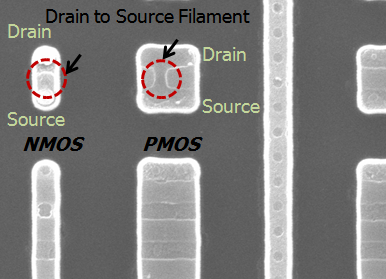 | Figure 2. SEM picture for the permanent damage in the source driver after ESD stress of IEC-Air 6kV |
 | Figure 3. Discharge path caught from the analysis result in the Figure 2 image |
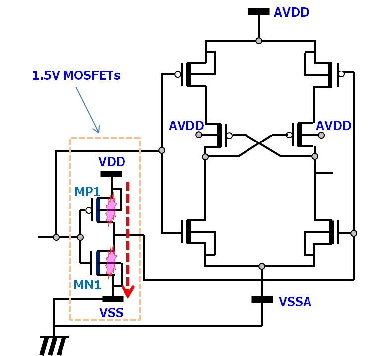
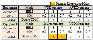
Figure 3 provides an overview of ESD discharge path around the damaged transistors in the level shifter block of the source driver. Damages were found at MP1 and MN1, supply voltages of which are biased to VDD 1.5V (regulated power in this chip) and VSS 0V at normal display operation status. Others in this figure are all made up of medium voltage transistors that are so called thick gate oxide transistors. Thin gate oxide transistors MP1 and MN1 are placed in front of low-to-high level shifter in order to transfer data signal from digital block to the differential inputs of the low-to-high level shifter. As shown in the Figure 2, damages are found at the MP1 and MN1 at the same time. Therefore, it is sufficiently possible to understand that discharge flow to the damage was made up from VDD to VSS through MP1 and MN1. Curiously enough, however, VDD or AVDD are not directly connected to the LCD panel where ESD stress is induced from gun. None of the devices in the diagram of Figure 3, of course, are directly connected to I/O pads. Therefore, to identify through what path ESD charge was injected deeply into VDD which is the bias for damaged transistors, reproduction tests were performed for the suspected I/O and power pins with various component level ESD testers and high level ESD stresses as shown below in Table 1. These tests were carried out using the evaluation package for display IC, even though commonly display driver IC is directly mounted on LCD module by the type of COG (Chip-On-Glass) without packaging. This is because various ESD pulses can be injected into each I/O or power pin, if it done with packaged driver IC.Table 1. Zapping table for identifying the culprit pin about the IC damage after system level ESD stress
 |
| |
|
Table 1 shows the HBM and MM ESD test results by ESD tester Mk.2 for VDD, AVDD, Source and VCOM pins[11],[12]. VDD and AVDD are the power pins used as the biases in the damaged block. Source pins are directly connected to the source drivers within the display driver IC and extended to the panel TFT through the transparent conductive oxide such as ITO (Indium-Tin-Oxide) in order to transfer data. VCOM is the common voltage pin for source driver and generally susceptible to on-chip ESD damage by ESD charge injected from LCD panel because it is located through the panel, and so plays a large role in charge coupling electrode. From the various tests in Table 1, it is seen that the source driver damage in Figure 2 can be reproduced only when source pin zapped by direct CDM method[13]. This means that ESD charge from LCD panel is coupled to the source pins and then the coupled charge leads to the damage of the thin gate oxide transistors MP1 and MN1 in Figure 3 which are connected between VDD and VSS. However, VDD and VSS are not the powers directly connected to the source pins. Figure 4 shows the voltage waveforms measured through VDD and AVDD pins during the ESD stress from gun into the source pin.The waveforms in Figure 4 reveal that the shape of VDD voltage waveform is very similar to that of AVDD except their different peak levels all over the measurement time. Therefore, through the test results in Table 1 and the voltage waveforms in Figure 4 (a), it is obvious that AVDD played a role in the stepping-stone between the charge injected from source pins and the thin gate oxide transistors MP1 and MN1 damaged due to the fluctuation of VDD during the ESD event. The display driver IC in this study was fabricated in a 0.09μm/30V HV CMOS process which supports various transistors having the typical voltage of 1.5V, 6V, 17V and 30V. The source driver block in Figure 3 consists of 1.5V and 6V devices which have trigger voltage (vt1) of ~6.5V and ~10V respectively. Therefore, the voltage waveforms shown in Figure 4 describes that the VDD fluctuation is threatening to damage the thin gate oxide transistors in source driver IC only within the early time of ~40nsec during the system level ESD event.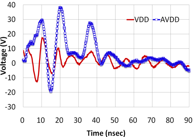 | Figure 4. Measured voltage waveforms of VDD and AVDD pin during the system level ESD stress (IEC-Air 8kV) for the source pin of display driver IC |
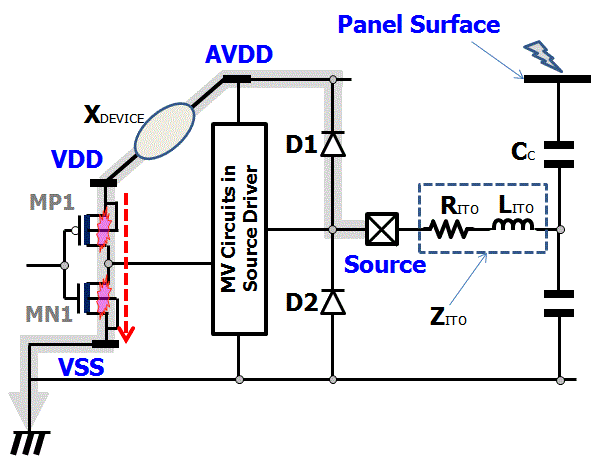 | Figure 5. ESD path from panel to ground through the damaged thin gate oxide transistors in source driver IC |
Figure 5 exhibits the detail ESD path from panel to ground through the damaged site. If ESD stress is induced into panel surface, charge can be coupled to source pins through the coupling element of CC between ITO and panel surface. ITO routing impedance for source channel is expressed by the lumped RLC parameter of RITO and LITO in Figure 5. Main ESD charge from source pins can arrive at AVDD node through the diode D1. In this situation, latent XDEVICE in Figure 5 must have delivered ESD charge from AVDD to VDD node since there is no intended ESD protection scheme or core circuitry between the two power nodes. In addition, damages in Figure 2 occurred only near the boundary of VDD biased NWELL facing with AVDD biased NWELL as shown in Figure 6.Figure 6 provides the layout picture around the damage site in source driver. In this figure 6, the upper side NWELL is biased by AVDD, while the lower side NWELL where ESD damages occurred is biased by VDD at display operation. These two NWELLs are drawn based on the minimum space design rule of 5um for compact layout and the p-sub guard-ring active biased by VGL (~-10V) level is arranged between the two NWELLs. In this technology, it is provided that the VGL should be connected to the p-sub all over the full chip. Cross section of A-A’ in Figure 6 is lined in order to address the coupling element of XDEVICE in the parasitic structure.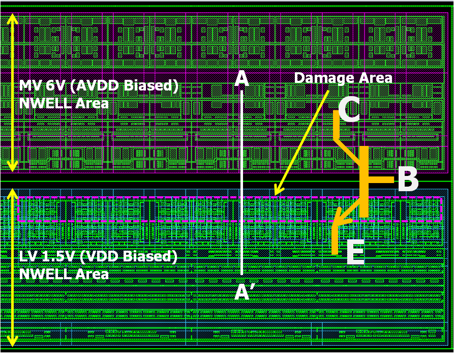 | Figure 6. Source driver NWELL areas (MV and LV NWELL) and damage site overview through the layout |
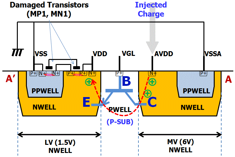 | Figure 7. Sketch for the cross section A-A’ in Figure 6: The parasitic NPN bipolar consists of NWELL (AVDD), PWELL (VGL) and NWELL (VDD) |
The sketch of Figure 7 indicates that ESD charge at AVDD can be coupled to VDD through the turn-on action of the XDEVICE (parasitic NPN bipolar) during the system level ESD event. The fact that system level ESD damage site (inside of asymptote in Figure 6) is weighted only toward the boundary of VDD-NWELL adjoining AVDD-NWELL demonstrates that the parasitic NPN bipolar action definitely led to the damages in the LV transistors biased by VDD. An important point to notice here is that BVCEO of NPN bipolar XDEVICE can be considerably low (half level of BVCBO in the worst case) because its base and emitter never can be shortened and they are connected to the completely different powers of VDD (1.5V) and VGL (~-10V). This means that BVCEO of the parasitic NPN bipolar is much lower than BVCBO and so the ESD charge from AVDD can be easily transferred to VDD.In this study, we can come to a conclusion that the hard failure after system level ESD stress came from the coupling effect between NWELL and its adjoining NWELL. Because the base node (VGL) of parasitic NPN bipolar has no choice but to be separated from emitter node (VDD), ESD charge can be easily transferred from AVDD to VDD through the parasitic bipolar turn-on action.
3. Failure Analysis (Soft Failure)
Usually, ‘soft failure’ by system level ESD test for the mobile LCD module can be classified as non-display and dot/line/block display defects. The soft failure features recovery to its original display status after reset operation. These kinds of display failure phenomena are widely well known to be due to the contamination of the logic or memory bit data stored at the normal display status before ESD stimulus.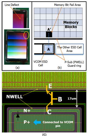 | Figure 8. Representative soft failure (line defect) phenomenon for mobile LCD module: (a) display phenomenon (b) sketch for the memory block arrangement around the memory bit failure site (c) layout image for the VCOM ESD cell and its adjoining memory block |
Figure 8 shows a simple soft failure case of mobile LCD module which occurred at the very low level of IEC-Air Mode-2kV (specified level is 6kV). It was analysed that this abnormal display of column line defect after ESD stress at the LCD panel is caused by the data contamination of the graphic memory (embedded in driver IC). As the result of tracking for the culprit memory block about this soft failure, it was found that the failure memory block is located in the vicinity of the specific ESD cell called by ‘VCOM’ which is on the major ESD discharge path from panel toward IC. In the common LCD module, VCOM node can be easily coupled to the injected charge from panel due to the structural feature as shown in Figure 9. Since the VCOM plane covers the entire area of the LCD panel, it can be regarded as a large plate of coupling capacitance CC between panel surface and common electrode. In other words, VCOM upper plane has a role in receiver antenna for ESD charge radiated from panel surface during the ESD event.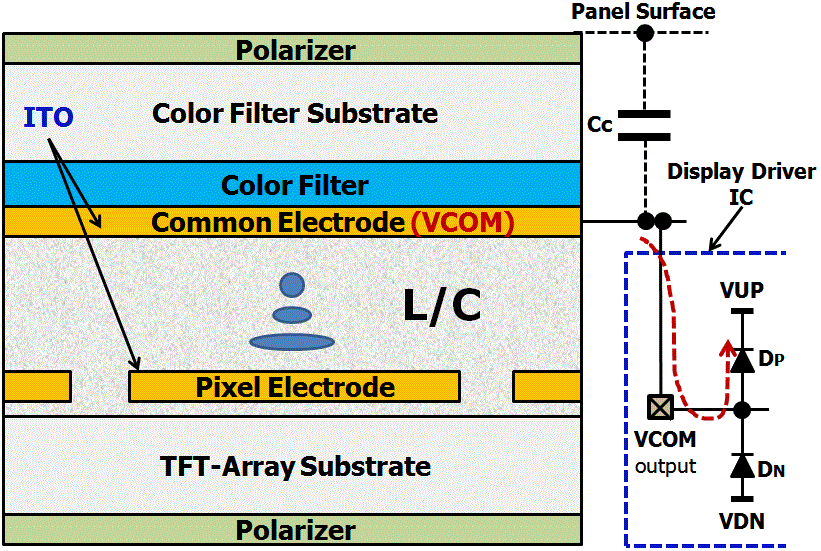 | Figure 9. Sketch for the LCD panel vertical structure including common electrode VCOM and its connection to driver IC |
As shown in Figure 9[14], VCOM ITO in LCD panel is directly connected to VCOM output pin in driver IC. Therefore, the majority of the coupled ESD charge to VCOM ITO can flow into the display driver IC though the VCOM output pin if there is no adequate bypassing to the system ground around the panel during the beginning stage of the ESD event. The layout image in Figure 8 (c) depicts the critical discharge path from VCOM pin to memory core based on the soft failure phenomenon in (a) and (b) of Figure 8. There can be insufficient space between the two NWELLs (in this failure analysis case, only 17um or so.) because IC shrinkage becomes more and more important with IC process technology advancing from the standpoint of manufacturer. Positive ESD charge induced from VCOM pin can easily discharge to VCOM ESD cell power (VUP in Figure 9) through the forward turn-on of diode DP as shown in Figure 9 (c). The parasitic NPN bipolar in Figure 8 (c) is composed of N-diffusion[Collector: N+/NWELL, VUP biased], P-diffusion[Base: PWELL (P-Sub), VGL biased.] and N-diffusion[Emitter: N+/NWELL, VDD biased] areas. The parasitic NPN bipolar turn-on action can lead to the large ESD charge transfer from I/O ESD cell to the memory core in the limited local area since VCOM electrode is a huge charging source against the IC despite its limited ESD cell pitch and height to several scores of micrometer. This proximity effect between the two different blocks is very similar to the previously presented case of hard failure in section A of chapter II.Memory data contamination (data transition from ‘0’ to ‘1’ or from ‘1’ to ‘0’) is possible, when VDD potential fluctuation for the memory occurs during the ESD event and it gives rise to the phase-out with its ground VSS, finally VDD and VSS node potential levels are reversed (commonly it is called as power upset). In practical design, memory power VDD is not directly connected to LCD panel because regulated power is usually used for the power. However, it is evident that soft failure easily occurs by VDD fluctuation during system level ESD event, in spite of its indirect connection with charge-initiated panel.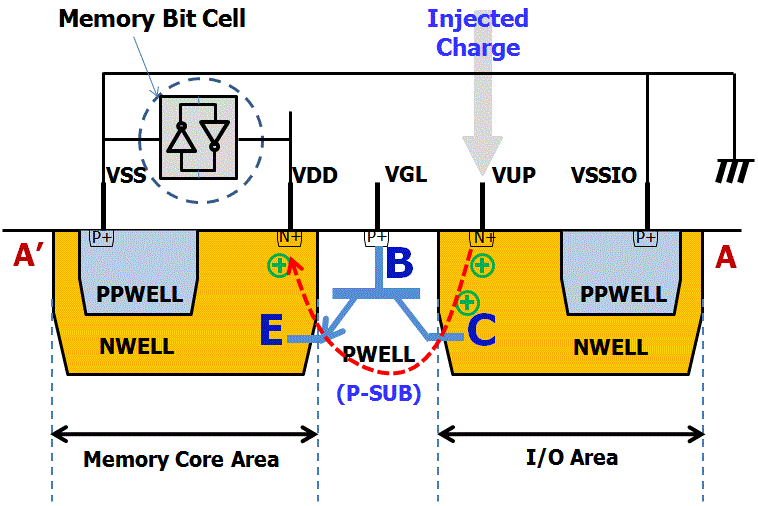 | Figure 10. Well formation sketch and bias notification for the A-A’ cross section shown in Figure 8 (b) |
Figure 10 shows the well formation focused on the soft failure site[A-A’ in Figure 8 (b)]. This driver IC was implemented by 30V HV CMOS process with the feature of triple well. In this structure, PWELL arranged outside of NWELL is not directly grounded, but negatively biased by VGL (~-10V). Each of NWELLs in core and I/O area is biased by VDD ~1.5V and VUP ~5V respectively in normal operation and there is no link between the two powers in ESD network. Power node potentials cannot help being fluctuated by external ESD stress originated from I/O (especially VCOM I/O in this study). Also, the injected charge into VUP can easily trigger the parasitic NPN bipolar between I/O and core, and therefore make VDD strongly coupled to VUP because the bipolar base-emitter impedance is very high.
4. On-Chip ESD Protection
Our analysis shows that the coupled amount of VDD potential in memory or logic block should be minimized during ESD event so as to prevent stored memory or logic data from transition. Figure 11 depicts a method which can mitigate coupled VDD potential effectively. In this figure, inserted deep NWELL (marked by dashed red box) plays a role as another emitter in the added parasitic NPN bipolar having high current gain due to the narrow base width compared to original parasitic NPN bipolar base. Most importantly, this structure enables ESD charge to be caught up toward ground, because NWELL is connected to ground node.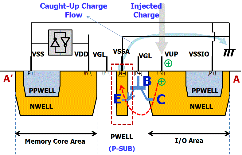 | Figure 11. Suggested scheme to mitigate VDD node potential |
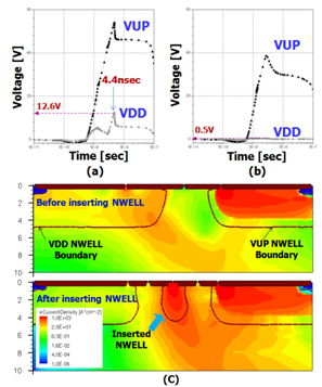 | Figure 12. Simulation result for Figure 10, 11 (a) before inserting grounded NWELL (b) after inserting grounded NWELL between I/O and core NWELLs (c) current density at the time of max. VDD (~4.4nsec) |
For more detail analysis, simulation structures for Figure 10 and Figure 11 were built up by TSUPREM4 2D and the mixed mode simulation for ESD event (IEC-61000-4-2 based) was carried out by MEDICI 2D[15]. Simulation result in Figure 12 reveals that VDD potential can be effectively reduced from max. 12.6V to 0.5V by inserting grounded NWELL catch-up guard-ring between VUP and VDD NWELLs.Alternative catch-up guard-ring structures shown in (a) and (b) of Figure 13 were simulated to verify the depth effect of the inserted n-type diffusion on the potential reduction during ESD event. As the result, VDD clamping voltages of 5.2V and 9.4V for (a) and (b) structure in Figure 13 explain that these structures are less effective than deep NWELL in Figure 11.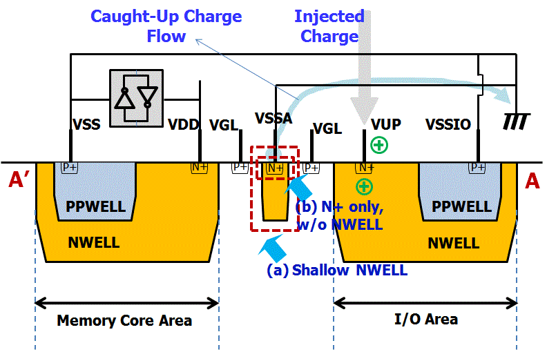 | Figure 13. Simulation result for Figure 10, 11 (a) before inserting grounded NWELL (b) after inserting grounded NWELL between I/O and core NWELLs (c) current density at the time of max. VDD (~4.4nsec) |
5. Conclusions
System level ESD is improved from ‘IEC-Air 2kV fail’ to ‘IEC-Air 6kV pass’ just by applying the catch-up guard-ring between I/O and core blocks with the other design factors fixed.The gap between I/O and core blocks (memory or logic which has storage capability) is more and more proactively narrowing as the chip size shrinkage is strongly requested. Therefore, it can’t be emphasized enough that coupling effect between I/O and core blocks should be mitigated to minimize the potential at the local area of logic or memory. Our study results on the hard and soft failures by system level ESD test are addressing one opportunity to overcome low level ESD under the severe situation of gap narrowing between ESD charging source and core.In our study, the damaged and contaminated sites during system level ESD stress are definitely not exposed. This analysis is noteworthy because it identifies a case where IC designers have to prepare on-chip ESD solution to the core circuit, even though it is not directly exposed to the IEC stress. In the current environment where IEC performance is being requested only on exposed pins with the hope that all system level issues will be addressed, this work shows that a more detailed strategy is required to ensure system level performance. Moreover, standard component level ESD analysis of the non-exposed pin was carried out to find the discharge path and correlate system level ESD damage.Parasitic NPN bipolar action causing both hard failure and soft failure was studied in this paper. Especially, we can know that the soft failure is an important observation, along with the observation that data integrity in the RAM is a very important to system level performance. Addition of guard-ringing to de-couple the parasitic NPN bipolar is suggested as a solution to the problem. The inserted guard-ring to catch up ESD charge is effective due to the fact that system level testing is performed with the ground pin connected to the system ground during the system level test.
ACKNOWLEDGEMENTS
Authors would like to thank the display driver IC circuit designer Jae-Sung Kang for his help to provide this study. We would also like to thank Min-Chang Ko and Kyoung-Ki Jeon for performing lots of ESD tests, failure analysis and waveform measurements, etc.
References
| [1] | ESD Industry Council, “System Level ESD Part I”, DECEMBER 2010. |
| [2] | Ki Hyuk Kim, Jeong-Hoi Koo, Bong-Gyu Kang, Soon Jae Kwon, Yongsup Kim, and Joongho Jeong, “Systematic design technique for improvements of mobile phone’s immunity to electrostatic discharge sof failures, IEEE International Symposium, JULY 2010. |
| [3] | Soon Jae Kwon, Ki Hyuk Kim, Yongsup Kim, and Austin. S. Kim, “Analysis of Mobile Phone’s Immunity to Electrostatic Discharge Soft Failures”, Asia-Pacific International Symposium on Electromagnetic Compatibility, APRIL 2010. |
| [4] | Jiang Xiao, David Pommerenke, Fan Zhou, James L. Drewniak, Hideki Shumiya, Takashi Yamada, and Kenji Araki, “Model for ESD LCD Upset of a Portable Product”, 2010 IEEE. |
| [5] | Douglas C. Smith, and Ed Nakauchi, “ESD Immunity in System Designs, System Field Experiences and Effects of PWB Layout”, EOS/ESD Symposium 2010. |
| [6] | Argha Nandy, “Prediction of soft error response of integrated circuits to electrostatic discharge injection via simulation field; Package interaction for electrostatic discharge soft error prediction; Full wave model for simulating noise ken electrostatic discharge generator”, Missouri University of Science and Technology, 2010. |
| [7] | Ming-Dou Ker and Cheng-Cheng Yen, “Transient-to-Digital Converter for System-Level Electrostatic Discharge Protection in CMOS ICs”, IEEE Transactions on Electromagnetic Compatibility, Vol. 51, NO.3, AUGUST 2009. |
| [8] | Giorgi Muchaidze, Jayong Koo, Qing Cai, Tun Li, Lijun Han, Andrew Martwick, Kai Wang, Jin Min, James L. Drewniak, and David Pommerenke, “Susceptibility Scanning as a Failure Analysis Tool for System-Level Electrostatic Discharge (ESD) Problems”, IEEE Transactions on Electromagnetic Compatibility, Vol. 50, NO.2, MAY 2008. |
| [9] | IEC61000-4-2, Electromagnetic Compatibility (EMC), “Part 4-2: Testing and measurement techniques – Electrostatic discharge immunity test”. |
| [10] | Ajith Amerasekera, Werner van den Abeelen, Leo van Roozendaal, Marcel Hannemann, and Paul Schofield, "ESD Failure Modes: Characteristics, Mechanisms, and Process Influences", IEEE Transactions on Electron Devices, Vol. 39, NO. 2, FEBRUARY 1992. |
| [11] | JEDEC standard, “Electrostatic Discharge (ESD) Sensitivity Testing Human Body Model (HBM)”, JEDEC Website. |
| [12] | JEDEC standard, “Electrostatic Discharge (ESD) Sensitivity Testing, Machine Model (MM)”, JEDEC Website. |
| [13] | Koen Verhaege, Guido V. Groeseneken, Herman E. Maes, Peter Egger, and Horst Gieser, “Influence of Tester, Test Method, and Device Type on CDM ESD Testing", in IEEE Transactions on Components, Packaging, and Manufacturing Technology - Part A, Vol. 18, NO. 2, JUNE 1995. |
| [14] | "The vertical structure of a color TFT LCD panel", Plasma.com Website. |
| [15] | “TSUPREM4/MEDICI 2D semiconductor process/device simulation user’s manual” Avant! Corp., Mountain View, CA, 1999. |
 Abstract
 Reference
 Full-Text PDF
 Full-Text HTML