-
Paper Information
- Next Paper
- Previous Paper
- Paper Submission
-
Journal Information
- About This Journal
- Editorial Board
- Current Issue
- Archive
- Author Guidelines
- Contact Us
Electrical and Electronic Engineering
p-ISSN: 2162-9455 e-ISSN: 2162-8459
2012; 2(5): 316-328
doi: 10.5923/j.eee.20120205.12
Fractional Spur Rejection and Area-Power Consumption Trade-off in ∑∆ Fractional-N PLL Design for Wireless Applications
 Abstract
 Reference
 Full-Text PDF
 Full-Text HTML
S. Sahnoun 1, A. Fakhfakh 1, N. Masmoudi 1, H. Levi 2
1LETI Laboratory University of Sfax, National Engineering School of Sfax Sfax, Tunisia
2IMS Laboratory University of Bordeaux I Bordeaux, France
Correspondence to: S. Sahnoun , LETI Laboratory University of Sfax, National Engineering School of Sfax Sfax, Tunisia.
| Email: |  |
Copyright © 2012 Scientific & Academic Publishing. All Rights Reserved.
RF systems are inherently complex multistage systems including principal functional blocks like mixer, limiter, RF amplifier, modulator, detector, etc. VHDL-AMS having the capabilities of modeling the systems at various levels of abstraction can be used for the modeling of RF systems. This paper proposes a high level design approach applied for the simulation and the optimization of modulators based on Phase Locked Loops (PLL). A simulation platform is developed using the hardware description language VHDL-AMS. Genetic algorithms and composite experimental designs are applied to minimize the lock time, the fractional spur rejection, the phase noise, the power consumption and the area of the designed modulator.
Keywords: Hierarchical Design, VHDL-AMS, Fractional-N PLL, Optimization, Genetic Algorithm, Experimental Designs, Lock Time, Spur Level, Phase Noise, Simulation Platform
Cite this paper: S. Sahnoun , A. Fakhfakh , N. Masmoudi , H. Levi , "Fractional Spur Rejection and Area-Power Consumption Trade-off in ∑∆ Fractional-N PLL Design for Wireless Applications", Electrical and Electronic Engineering, Vol. 2 No. 5, 2012, pp. 316-328. doi: 10.5923/j.eee.20120205.12.
Article Outline
1. Introduction
- The wireless communication market is undergoing a major expansion with the deployment of new technologies and standards opening the prospect of significant impacts in many application areas (security, health, automobile, telecommunications, robotics…). The emerging wireless technologies require architectures with reduced complexity, cost and power consumption; however, they require more accuracy and performance of specific circuits.This evolution pushes designers both to find new architectures of circuits and systems which can offer high performance, low-cost and low power consumption, and also to use new CAD (Computer-Assisted Design)methodologies able to model the mixed-mode behavior (analog / digital) of these systems. Currently, the hardware description language is widely applied in the design of mixed-signal circuits. Indeed, the VHDL-AMS standard allows the implementation of the top-down hierarchical approach for analog and mixed systems[1,2,3]. Therefore, it can be used for behavioral modeling and design of phase locked loop (PLL), which is a key element for any wireless communication system. Standard PLL frequency synthesizers with integer–N and channel spacing. The fractional-N technique offers wide bandwidth with narrow channel spacing and alleviates phase locked loop (PLL) design constraints for phase noise. The ∑∆ fractional-N PLL[4, 5] is attractive for frequency synthesis or direct modulation. This architecture can still meet requirements such as low-power consumption and simple topology, and is suitable for high-level integration.The design of fractional-N PLL synthesizers, however, requires an iterative design process due to the large set of system parameters that must be optimized to achieve the desired phase noise, settling time, and fractional spur rejection. In addition, a ∑∆ modulator used toinstantaneously alter the feedback division modulus introduces excessive phase noise and fractional spurs. A behavioral level simulator is required to reduce the design runtime as well as assess the phase noise contribution and fractional spur rejection of the ∑∆ modulator before the physical design phase. In the literature many papers have studied the implementation of the behavioral models of classical PLL systems and ∑∆ synthesizers[6, 7, 8].However, there are few works that show the full analysis and design of ∑∆ synthesizers using behavioral modeling. In this paper, a ∑∆ fractional-N PLL is modeled using VHDL-AMS and synthesized for a wireless application. For this study, many HDL models have been studied and tested for different PLL blocks. A comparison with transistor-level simulations validates the proposed models.This paper is outlined as follows. In section 2, we detail the proposed hierarchical design flow. In section 3, we describe how to determine the modulator parameters. In section 4, we detail the high level description of the studied system. In sections 5, we present a second optimization step to improve the lock time with experimental designs. In session 5, we detail the modulator characterization. Section 6 draws a conclusion.
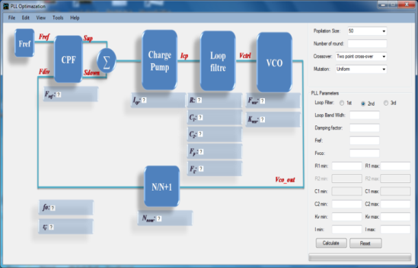
2. The Proposed Hierarchical Design Flow
- The common method for the PLL loop filter design starts by deciding a frequency range, a channel spacing and N counter value. Then, we choose arbitrary the values for filter parameters, calculate filter components and then analyze. If the loop filter does not meet lock time and spurious requirements, then we adjust parameter values and re-optimize. The disadvantage of this common method is that it is an iterative process, very time consuming and based on trial and error. Furthermore, it does not always achieve the optimal solution.Dean Benerjee et all propose in[9] a new approach which reduces the number of iterations to do. With this approach, we give the frequency range and the channel spacing. The N counter value is the consequence of these two parameters. We then come up with system requirements especially lock time and spur level. Once we have an idea of these requirements, we select the charge gain, the Voltage Controlled Oscillator (VCO) gain and the VCO input capacitance.An intelligent algorithm helps to converge to the best solution and then calculates the filter components to meet the lock time and the spur level requirements. The proposed new approach was applied to develop “Easy PLL” software. Easy PLL basically allows to set system requirements, determine loop filter’s components and then do simulations to examine various types of waveforms.In[10], Antonio Calaci et al propose a systematic analysis and optimization of analog and mixed signal circuits balancing accuracy and design time. In fact, since both systematic sizing approaches and statistical analysis require many simulations, Antonio Calaci applies a hierarchical approach with different levels of simulation and accuracy from system to transistor level to balance the tradeoff between time and accuracy. All sizing and optimization steps are driven by WiCkeD[11], an EDA environment independent tool for circuit analysis and sizing. WeiCkeD does statistical optimization with a unique deterministic worst-case distance algorithm.M. Henderson Perrott uses VppSim software environment to compute the PLL parameters[12]. VppSim provides a software framework that supports Verilog and C++ co-simulation within the Cadence environment. VppSim therefore provides a top-down design methodology in which designers start at the highest level with CppSim modules, and then gradually build more granular models using Verilog and Spectre. Designers can also benefit from the ability to convert CppSim systems created within Cadence into Matlab or Simulink functions.In our case, we developed a simulation platform to simulate ∑∆ fractional-N PLLs acting as a direct modulator. The hierarchical design flow we use is detailed in Figure 1. First, the phase noise specification is fixed, and then the PLL bandwidth is calculated. With CppSim, we compute the PLL parameters. An initial solution is obtained which respects the phase noise constraints. However, the PLL is not necessary a fast locking one. For this reason, we developed an optimization interface based on a genetic algorithm to converge to a faster PLL. At this step, only a functional PLL model is employed. In a second step, fractional-N PLL is described in VHDL-AMS and simulated in Simplorer 7.0 software. The PLL lock time and the spur rejection are simulated with the optimized solution. If the required specifications are not reached, a second optimization based on experimental designs is done.Compared to previous works, the hierarchical design flow we propose presents the following advantages: first phase noise specifications are respected when calculating the different PLL parameters. Second, we show that it is possible to improve the solution obtained with CppSim when adding an optimization interface based on a genetic algorithm. Third, the second optimization based on experimental designs helps to converge to a better solution after doing few simulations with a multi-abstraction VHDL-AMS description of the fractional-N PLL.
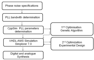 | Figure 1. The proposed hierarchical design flow |
3. Determination of the Modulator Parameters
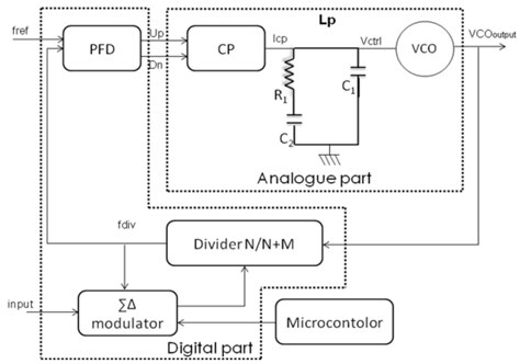
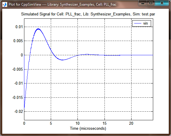
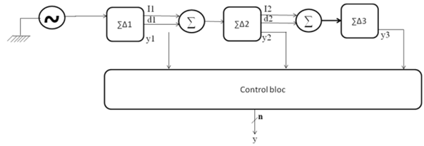
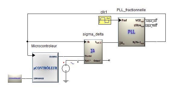
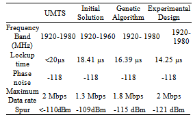
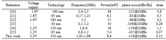
- Figure 2 shows the block diagram of the studied modulator[13-14]. It is a mixed system composed of both analogue and digital parts. It is based on a fractional-N frequency synthesizer directly modulated at high data rate with a ∑Δ modulator. This technique achieves good noise performance. In fact, it allows digital phase/frequency modulation to be achieved at high data rates without mixers or D/A converters in the modulation path.The synthesizer is implemented as a PLL. To achieve good noise performance with a simple design, the PLL bandwidth is set to a low value relative to the data bandwidth. To illustrate our design approach, the described modulator is used to build a 1.92 GHz to 1.98 GHz transmitter respecting the Universal Mobile Telecommunications System (UMTS) standard[14].Our target consists in reducing the PLL lockup time, maintaining reduced spur level and phase noise and having a capture range covering the UMTS frequency band.
 | Figure 2. Block diagram of the modulator |
3.1. Pll Parameters Determination with Cppsim
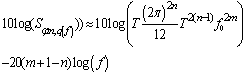
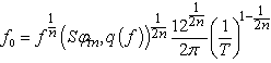
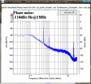
- Table 1 resumes the main parameters of the modulator (Icp, R, C1, C2 and Kvco). With the help of CppSim system simulator, we start our design flow by extracting initial values of these parameters. In this case, we compute the bandwidth of the PLL, and CppSim extracts the open loop parameters as shown on Figure 3.The PLL bandwidth f0 is calculated in order to achieve a phase noise respecting the UMTS specification (less then -118 dBc/Hz@1MHz). The phase noise performance can be separated into two components: intrinsic noise and quantization noise. Intrinsic noise is due to circuit elements present in any PLL, including reference input jitter, reference feed through, charge-pump noise, and VCO phase noise. Quantization noise, which is caused by dithering, is particular to fractional-N synthesizers. The power spectral density (PSD) of the quantization noise appearing at the output of the synthesizer (after being filtered by the PLL dynamics) can be expressed by the following noise model[13]:
 | (1) |
 | (2) |
 = -118 dBc/Hz, we obtain f0 = 84 kHz.Table 1 shows the obtained values for the different parameters of the modulator.
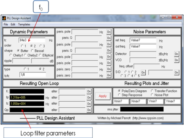 | Figure 3. PLL design interface |
 | Figure 4. Loop filter response with Sue2 |
|
3.2. Optimization with Genetic Algorithm
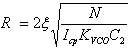
- The optimization algorithm we use is based on a genetic algorithm[15] and developed in Visual Basic. The algorithm builds an initial population of possible solutions. It evaluates the performance of each and assigns it a corresponding value referred as fitness. It then selects the better solutions from the population, applies variation operators to them to create a new population for the next generation and iterates.Figure 5 shows the optimization interface we developed: on the left, the optimization parameters are listed (representing the bandwidth f0 and the damping factor ξ). On the right, we can see the different genetic algorithm characteristics fixed as following: number of generations: 100, individuals: 10, runs: 1000, selections: 5, mutations: 5.We also defines the range of variation for each parameter of the PLL (ICP, R, C1, C2 and KVCO)When applying genetic algorithm, the two key parameters are the number of generations NG and the population size Np. If the population is too small, there will not be sufficient diversity in the strings to find the optimal string by a series of operations. If the number of generations is too small, there will not be enough chances to find the optimum. These two parameters are not independent. The larger the population is, the smaller the number of generations needed to have a good chance of finding the optimum is. Moreover, the optimum is not guaranteed; there is just a good chance of finding it.We optimize the lock time Tr in order to make the PLL faster and then to apply a higher input data rate. Two constraints are introduced: the damping factor ξ and the bandwidth f0 should be respectively close to 0.707 and 84 kHz. In this case, we can guarantee low spur and low phase noise. We apply the method proposed by Ken Holladay[16]. The different optimization factors (R, C1, C2, Icp and Kvco) are related to Tr and ξ as follows:
 | (3) |
 and lcp the UMTS canal width.
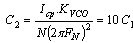 | (4) |
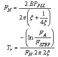 | (5) |
 and FA=1000 KHz. The obtained optimized solution is shown on Table 3:
|
|
 | Figure 5. PLL optimization interface |
 | Figure 6. Modulator phase noise characteristic |
 | Figure 7. Loop filter output corresponding to the UMTS frequency band |
4. High Level Description of the Modulator
- CppSim library contains pre-compiled models described in Verilog-A. We used these models to simulate the modulator in Sue2. But when going down in the hierarchical design flow, we should select a transistor level topology for each block constituting the modulator. To reduce the CPU runtime, the modulator is not simulated at the transistor level but each bloc is described in the hardware description language VHDL-AMS.
4.1. Digital Part Modeling
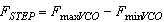
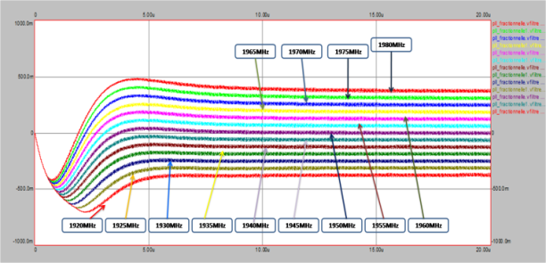
- The modulator is simulated in CMOS 350 nm technology. The behaviours of digital building blocks are characterized using delay and slew and included in the behavioural simulation flow. The digital part contains a phase frequency detector (PFD), a Sigma Delta modulator and a N/N+M frequency divider. The reference frequency FREF is fixed at 26 MHz. To achieve an output frequency varying between 1,92 GHz and 1,98 GHz, the frequency divider ratio should vary between 73.85 and 76.15.
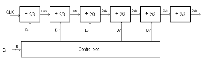 | Figure 8. The frequency divider topology |
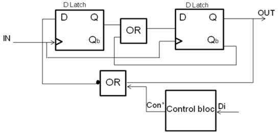 | Figure 9. The 2/3 divider bloc topology |
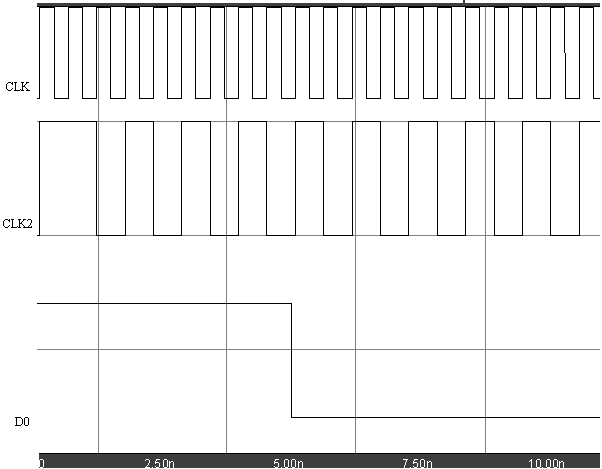 | Figure 10. The 2/3 divider simulation |
 The PFD topology is depicted on Figure 11. It is mainly composed of D latches. It was described with a VHDL code.
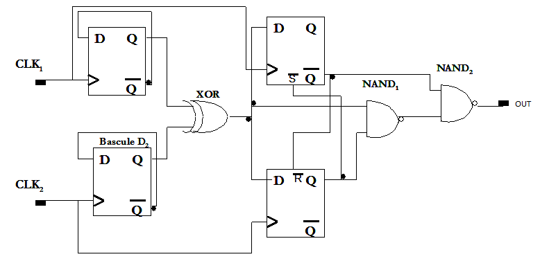 | Figure 11. The phase frequency detector topology |
 | Figure 12. Sigma Delta modulator topology |
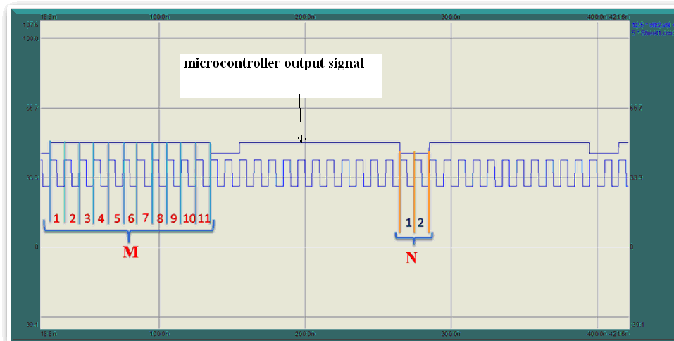 | Figure 13. Microcontroller output signal |
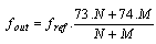 | (6) |
|
 | Figure 14. Power consumption by a digital part |
4.2. Analogue Part Modeling
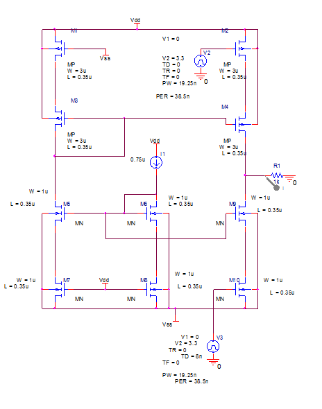 | Figure 15. Charge pump transistor level topology |
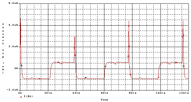 | Figure 16. Output current of the charge pump |
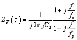 | (7) |
 and
and with fZ
 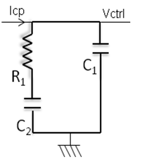 | Figure 17. Passive loop filter topology |
 | (8) |
4.3. Modulator Simulation
- In order to validate the ability of VHDL-AMS to successfully describe the modulator performance, a common and complex mixed-signal model has been developed. By using VHDL-AMS, the architecture of each block has been defined and simulated. The CP, the loop filter and the VCO are modeled in VHDL-AMS. The PFD, frequency divider and ∑∆ modulator are lumped into a single model in VHDL. These two parts are simulated under Simplorer 7.0 as illustrated in Figure 20.
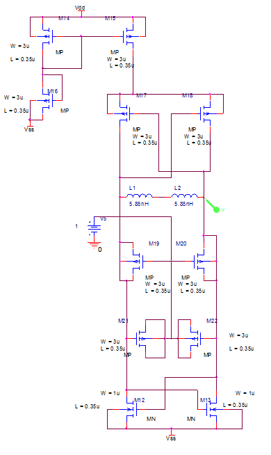 | Figure 18. VCO transistor level topology |
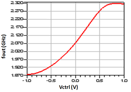 | Figure 19. VCO transfert function |
 | Figure 20. The modulator simulation in Simplorer environment |
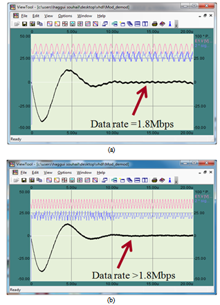 | Figure 21. Demodulator response |
5. Second Step Optimization
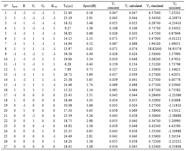
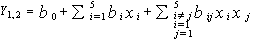
- With the first optimization using the genetic algorithm, the optimization interface uses an ideal and functional model of the modulator. To find a better solution around the optimized topology, we apply a second optimization step based on experimental designs.The most frequent designs in optimization problems involving three or more factors are central composite ones, Box-Behnken designs, D-optimal designs, and others, such as Hoke designs[18]. Central composite designs and Box-Behnken designs are the most appropriate to detect curvatures in a multidimensional space, but require a large number of experiments beyond three factors. D-optimal designs are less frequent, but adequate in cases involving linear functions where the factors can only be varied over a restricted area, and thereby creates an irregular experimental domain in which orthogonality cannot be achieved. Hoke designs are economical second-order designs based on irregular fractions of partially balanced type of the 3k factorial for a number of factors k ≥ 3.In this work, we consider that the experimental region is a hypercube and we apply a five factor central composite design. Considering that the efficiency of any experimental design is defined as the number of coefficients of the model divided by the number of experiments, central composite design is the most efficient compared to Hoke-D4, Box-Behnken or Doehlert designs. Central composite designs are also more efficient in mapping space: adjoining hexagons can fill a space completely and efficiently, since the hexagons fill space without overlap. The objective of this optimization step is to reduce the PLL lockup time in order to reach an input data rate of 2 Mbps for the designed modulator. The spur level should be maintained as low as possible.The experimental designs as a function of the selected main factors have to be determined. The lock time and the spur level of the PLL are in trade-off relationship with each other. The analysis of results and the building of experimental designs are carried out with the NEMRODW mathematical statistical software[19].We apply the experimental design with three levels. In this case, the effect of each factor is studied according to three different values to which we attribute levels +1, 0 and –1 corresponding respectively to the maximum, the middle and the minimum values as illustrated on Table 6.
|
|
 | (9) |
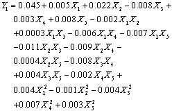 | (10) |
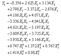 | (11) |
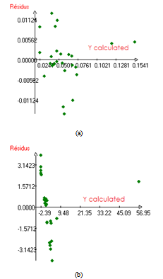 | Figure 22. Residus Variation (a) Y1, b) Y2) |
|
6. Modulator Characterization
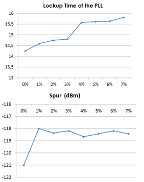
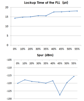
- When increasing the VCO no linearity coefficient A, the lockup time and the spur level increase as shown on Figure 23. To maintain a low lockup time, we need A to be less than 3% whereas to maintain a low spur, A should be less than 1%.In a second characterization, we can see in Figure 24 the variation of the lockup time and the spur with the dissymmetry coefficient of the charge pump. The design of an efficient modulator needs the current dissymmetry to be less than 35% to have a reduced lockup time and to maintain a low spur level.
 | Figure 23. Lockup time and Spur level variation with A coefficient |
 | Figure 24. Lockup time and Spur level variation with dissymmetry coefficient |
|
7. Conclusions
- The proposed paper has demonstrated the behavioral modeling and systematic mixed-design of ∑∆ fractional-N PLL acting as a direct modulator using hardware description language VHDL-AMS. The behavioral modeling can provide a fast estimation of PLL performances compared to transistor-level simulation. These HDL behavioral models can be successfully mixed with some circuit blocks (transistor-level) to rapidly evaluate the contribution of each noise source and non-ideal element. This can help designers to test ∑∆ fractional-N PLLs, for a given wireless application, accurately within a minimum CPU time. With the help of an optimization interface based on a genetic algorithm, we can achieve a faster modulator making possible to apply a higher input signal rate and to respect the phase noise limitation of the UMTS standard. A second optimization step based on experimental designs helps to converge to a better optimal solution.Many computer aided design software are employed to achieve a hierarchical design flow. Our target consists in helping to develop new analogue synthesis techniques to support a future high-level mixed-signal synthesis environment.
References
| [1] | Design Automation Standards Committee of the IEEE Computer Society, IEEE Standard VHDL Analog and Mixed Signal Extensions. - 314 pages, Doc., IEEE Std 1076.1-1999, 18 March 1999. |
| [2] | Gregory Peterson, Peter J. Ashenden, Darrell A. Teegarden, The System Designer's Guide to VHDL-AMS: Analog, Mixed-Signal, and Mixed-Technology Modeling, Morgan Kaufmann Publishers; 2002. |
| [3] | Y. Hervé, VHDL-AMS: applications et enjeux industriels, Dunod, Paris 2002. |
| [4] | T.A. Riley, M. A. Copeland. Delta-Sigma Modulation in Fractional-N Frequency Synthesis. In IEEE J. Solid State Circuits, vol. 28, pp. 553- 559, May 1993. |
| [5] | M.H. Perrott, T.L. Tewksbury, and C.G. Sodini, A 27-mW CMOS fractional-N synthesizer using digital compensation for 2.5-Mb/s GFSK modulation. IEEE J. Solid-State Circuits, vol.32, no.12, pp.2048–2060, Dec. 1997. |
| [6] | M. Hinz, I. Konenkamp and E.H. Horneber. Behavioral Modeling and Simulation of Phase-Locked Loops for RF Front Ends. In IEEE Midwest Symp. On Circuits and Systems, pp. 194-197, Aug. 2000. |
| [7] | N. Milet-Lewis, G. Monnerie, A. Fakhfakh, and all. A VHDL-AMS library of RF blocks models. IEEE International Workshop on Behavioral Modeling and Simulation, 12 – 14, 2001. |
| [8] | M.H. Perrott, Fast and accurate behavioral simulation of fractional-N frequency synthesizers and other PLL/DLL circuits, Proc. 39th Design Automation Conf., pp.498–503, June 2002. |
| [9] | D Banerjee, D Brown, K Nguyen “Loop Filter Optimization”, National Semiconductor, the Sight & Sound of information, http://www.national.com/AU/design/loop_filter_optimization.pdf. |
| [10] | A Calaci et al, “Systematic Analysis & Optimization of Analog/Mixed-Signal Circuits Balancing Accuracy and Design Time”, SBCCI’10, September 6-9, 2010, Sao Paulo, SP, Brazil. |
| [11] | G Strube, “Robuste Verfahren zur Worst-Case-und-Ausbute-Analyse analog integrierter Schaltungen”, Hieronymus Munchen, 1998, ISBN 3-933083-52-4. |
| [12] | Michael H. Perrott “PLL Design Using the PLL Design Assistant Program” http://www.cppsim.com July 2008. |
| [13] | M. H. Perrott, Theodore L. Tewksbury III, Charles G. Sodini, «A 27-mW CMOS Fractional- Synthesizer Using Digital Compensation for 2.5-Mb/s GFSK Modulation», IEEE journal of solid-state circuits, vol. 32, no. 12, december 1997. |
| [14] | C. Fourtet «Modulation double port FSK/GFSK pour une utilisation en DECT ou liens radio digitaux» Motorola Semiconducteurs S.A. Centre Electronique de Toulouse. |
| [15] | J. H. Holland, Adaptation in natural and artificial systems. Ann Arbor : The University of Michigan Press, 1975. |
| [16] | K Holladay, « Design a PLL for specific loop bandwidth »,END EUROPE,pp 64-66,October2000,http//:www.ednmag.com. |
| [17] | S. Eloued, A. Fakhfakh and N. Masmoudi “Analogue synthesis methodology using VHDL-AMS application to a frequency synthesizer design”, SSD07, Tunisia. |
| [18] | T. Lundstedt, E. Seifert, L. Abramo, B. Thelin, Å. Nyström, J. Pettersen, and R.Bergman, Experimental Design and optimisation, Chemometr. Intell. Lab. Syst., 42 (1998) 3-240. |
| [19] | D. Mathieu, J. Nony, R. Phan-Tan-Luu, ”NEMROD-W software”, LPRAI, Marseille, 2000. |
| [20] | K. Wang, A. Swaminathan, and I. Galton, “Spurious -Tone Suppression Techniques Applied to a Wide-Bandwidth 2.4GHz Fractional-N PLL,”Solid-State Circuits Conference, 2008. ISSCC 2008. Digest of Technical Papers. IEEE International, pp. 342–618, 2008. |
| [21] | X. Yu, Y. Sun, L. Zhang, W. Rhee, and Z. Wang, “A 1GHz Fractional- N PLL Clock Generator with Low-OSR ΣΔ Modulation and FIREmbedded Noise Filtering,” IEEE International Solid-State Circuits Conference, pp. 346 – 618, 2008 |
| [22] | S.-Y. Lin and S.-I. Liu, “A 1.5 GHz All-Digital Spread-Spectrum Clock Generator,” IEEE Journal of Solid-State Circuits, Volume: 44 , Issue: 11, pp. 3111 – 3119, 2009. |
| [23] | J. Borremans, K. Vengattaramane, V. Giannini, B. Debaillie, W. Van Thillo, and J. Craninckx, “A 86 MHz-12GHz digital-intensive PLL for software-defined radios, using a 6 fJ/step TDC in 40nm digital CMOS ,” IEEE Journal of Solid-State Circuits, Volume: 45, Issue: 10, pp. 2116 – 2129, 2010. |
| [24] | D. H. Huang, J. Zhou, W. Li, N. L. Li, and J. Ren, “A fractional-N synthesizer for cellular and short range multi-standard wireless receiver ,” International Symposium on Circuit and System, pp. 2071 – 2074, 2010. |
| [25] | Y. Zhang, N. Zimmermann, R. Wunderlich and S. Heinen, “A Wide-Frequency-Range Fractional-N Synthesizer for Clock Generation in 65nm CMOS”, 978-1-4577-1846-5/11/$26.00 ©2011 IEEE PP 571-575, ICECS 2011. |
| [26] | L. Burciu, « Architecture de récepteurs radiofréquences dédiés au traitement bibande simultané », PhD thesis, 2010. |