-
Paper Information
- Next Paper
- Previous Paper
- Paper Submission
-
Journal Information
- About This Journal
- Editorial Board
- Current Issue
- Archive
- Author Guidelines
- Contact Us
Electrical and Electronic Engineering
p-ISSN: 2162-9455 e-ISSN: 2162-8459
2012; 2(5): 309-315
doi: 10.5923/j.eee.20120205.11
2D Simulations of Current-voltage Characteristics of Cubic AlxGa1-xN/GaN Modulation Doped Hetero-junction Field Effect Transistor Structures
 Abstract
 Reference
 Full-Text PDF
 Full-Text HTML
Driss Bouguenna 1, A. Boudghene Stambouli 2, A. Zado 3, D. J. As 3, N. Mekkakia Maaza 2
1Department of L.M.D SM, Faculty of Sciences & Technology, University of Mascara, 29000, Mascara, Algeria
2Electrical Engineering Laboratory of Oran, Department of Electronics, Faculty of Electrical & Electronics Engineering, University of Sciences & Technology of Oran, 31000, Oran, Algeria
3Department of Physics, Faculty of Science, University of Paderborn, Warburger Str. 100, 33095 Paderborn, Germany
Correspondence to: Driss Bouguenna , Department of L.M.D SM, Faculty of Sciences & Technology, University of Mascara, 29000, Mascara, Algeria.
| Email: |  |
Copyright © 2012 Scientific & Academic Publishing. All Rights Reserved.
We report on calculations of the current-voltage characteristics of cubic AlxGa1-xN/GaN modulation doped hetero-junction field effect transistors using two-dimensional nextnano3 device simulation software. Specifically, we investigate the influence of the thickness and the background doping concentration of cubic GaN buffer on the output and transfer characteristics of the device. Also, the influence of Al content and the effect of a  -doped layer inserted in the AlxGa1-xN are discussed. We find that the maximum saturation current is shown by a structure with a
  -doped layer of n = 6 x 1018 cm-3, Al content of x = 25% and a GaN buffer layer thickness of 100 nm. For this structure, our calculations show a low threshold voltage value and the highest transconductance gm among the sample structure that we used for our calculations.
Keywords: Cubic AlxGa1-xN/GaN, MODFET, Δ-doping, Drain Current, Threshold Voltage, Nextnano3
Cite this paper: Driss Bouguenna , A. Boudghene Stambouli , A. Zado , D. J. As , N. Mekkakia Maaza , "2D Simulations of Current-voltage Characteristics of Cubic AlxGa1-xN/GaN Modulation Doped Hetero-junction Field Effect Transistor Structures", Electrical and Electronic Engineering, Vol. 2 No. 5, 2012, pp. 309-315. doi: 10.5923/j.eee.20120205.11.
Article Outline
1. Introduction
- The reduction of dimensions in electronic devices such as high electron mobility transistors may allow higher transfer rates in data communication systems[1]. AlxGa1-xN/GaN based high electron mobility transistors (HEMT) have shown great potential for high-frequency and high-power applications. In fact, AlxGa1-xN/GaN HEMTs exploit the advantages of the wide band gap GaN materials, namely high mobility and high carriers density reached by the two dimensional electron gas (2DEG) formed at the hetero-interface[2]. This is motivated by their potential in commercial and military applications, e.g., in the area of telecommunication systems, base stations market, as well as radar, W-CDMA mobile-phone applications[3],[4], high temperature electronics, high power solid state switching, and hard radiation in space electronics.However, the cubic nitrides would allow using the same technology for normally-on and normally-off devices[5]. So far, the important problem is transconductance (gm) decrease due to a large parasitic resistance[6],[7] in normally-off MODFETs devices, and shows result of large gate leakage current and current collapse, which is mainly due to the cubic AlxGa1-xN surface under the gate. The development of these devices, is still hindered by some problems including large gate leakage current[8],[9] drain current collapse[10] at high frequencies, and poor long-term reliabilities of the Schottky gate. Large gate leakage affects the device’s noise level, especially at elevated temperature when gate leakage increases significantly[11] whichever with some problems including gate leakage, current collapse, reliability, and yield.In addition, cubic AlxGa1-xN/GaN MODFETs with normally-on and normally-off output and transfer characteristics depending on the doping concentration, the thickness of the buffer layer and Al content of the AlxGa1-xN barrier were demonstrated. The devices are simulated by I-V characteristics using two-dimensional nextnano3 device simulation software. The sample structures for improved cubic AlxGa1-xN/GaN MODFET devices were developed. In this paper a direct methodology to investigate the influence of the thickness and the background doping concentration of cubic GaN buffer on the I-V characteristics of the device. Also, the influence of Al content and the effect of a
 -doped layer inserted in the AlxGa1-xN are discussed. Our device exhibits maximum drain source saturation current of IDSsat = 130 A/m for x = 25% and clear field-effect at positive bias voltages with threshold voltage of Vth = 0.4 V compared with the results similar which obtained by Saint Martin et al, for double gate MOSFETs[12].
2. Basics of HEMTs
- The unique feature of HEMT device is the hetero-structure interface where a two dimensional electron gas channel is formed. Also due to this modulation doping, carriers diffuse into the undoped hetero-interface[13]. To avoid impurity scattering, the carriers are spatially separated from the doped region using a thin (1 - 5) nm AlxGa1-xN spacer layer. The idea of the modulation doped structure was proposed at Bell Laboratories in the late 1970s[13] and then in 1978, Dingle et al. first demonstrated enhanced mobility in the AlxGa1-xAs/GaAs modulation doped super-lattice structure[14]. In 1979 Stormer et al. subsequently reported similar effect using a single AlxGa1-xAs/GaAs hetero-junction[15]. These studies were made on two-terminal devices without the control gate. This effect was applied to the field-effect transistor by Mimura et al. in 1980[16],[17] and later by Delagebeaudeuf et al. in the same year[18]. Since then, the HEMT has been the topic of major research activities and has matured to commercial products as an alternative to MESFETs in high-speed circuits[19-22]. However, these basic characteristics of AlxGa1-xAs/GaAs HEMTs are also essentials to AlxGa1-xN/GaN modulation doped hetero-junction field effect transistors (MODFETs) in order to understand their bases.The main advantage of modulation doping is the elimination of traps in the AlxGa1-xN layer and of the parallel conduction path within this doped AlxGa1-xN layer. This is due to decreased parasitic channel in the AlxGa1-xN layer. Thereby, the mobility of transistors is superior. The bulk mobility as a function of temperature shows a peak at a certain temperature. The decrease of bulk mobility with increase of temperature is due to phonon scattering. At low temperatures, the bulk mobility is limited by impurity scattering. It depends, as expected, on the doping level and it also decreases with a decrease of temperature. In the modulation-doped channel, mobility at temperatures above ≈ 80 K is comparable to the value of a low doped bulk sample. However, mobility is much enhanced at lower temperatures[23].
2.1. Basic Device Structure
- A basic MODFET structure based on the AlxGa1-xN/GaN system is shown in Figure 1. It can be noted that the barrier AlxGa1-xN layer under the gate is doped, while the GaN buffer layer is undoped. The doped barrier layer is typically around 20 nm thick. Very often, instead of uniform doping, a δ-doped charge sheet is used within the barrier layer and placed close to the channel interface. The source and drain contacts are ohmic, while the gate is a Schottky barrier. Sometimes, the top layer of n+-GaN on AlxGa1-xN is used for better source and drain ohmic contacts. The deeper n+-regions of source/drain are formed either by ion implantation or introduced during the alloying step to contact the electron channel. For low values of drain-to-source bias, the current flows from drain-to-source through the electron channel. The carrier sheet density and consequently the conductivity of the channel are controlled by the gate bias. Increasing of the positive bias applied to the gate increases the depth of the potential well at the AlxGa1-xN/GaN interface. This results in enhanced sheet carrier density of the electron channel, therefore increasing current conduction. On the contrary, increasing of the negative gate bias decreases the depth of the electron channel and the sheet carrier density decreases, thereby lowering the channel conductivity.In the device geometry, the most-important parameter is the gate length LG. This dimension determines the maximum frequency limits for MODFET devices. Typical gate lengths are in the 0.1... 2 μm range. The gate width Z is another physical device dimension that is of primary importance to the determination of device behavior. The device current is directly proportional to the gate width because of the cross section area, available for the channel current, is proportional to Z. For low noise and low current applications, devices with relatively small gate width are utilized. In contrast, large gate width devices are typically used for power applications. Other characteristic dimensions are: the gate-to-source LGS, gate-to-drain LGD spacing, the drain LD and source length LS.
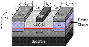 | Figure 1. Typical structure of MODFET using the basic AlxGa1-xN/GaN system |
2.2. Current-Voltage Characteristics
- In this work, n-channel devices based on cubic AlxGa1-xN/GaN with a two dimensional channel formed by electrons were calculated. There are two different types of FETs depending on the state of the transistors with zero gate bias. Their schematic output and transfer characteristics are shown in Figure 2. The energy band diagrams at equilibrium (calculated for a cubic AlxGa1-xN/GaN hetero-structure) are illustrated in Figure 3. FETs are called enhancement-mode or normally-off if at zero bias the channel is depleted and the Fermi level EF is below the conduction band edge EC. In this mode the conduction of the electron channel is very low and a positive gate voltage must be applied to populate the channel with carriers. The counterpart is called depletion mode, or normally-on, if the channel is conductive for zero gate bias. The Fermi level EF crosses the conduction band edge at the AlxGa1-xN/GaN hetero-interface. Negative gate voltage must be applied to turn the transistor-off.
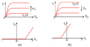 | Figure 2. Comparison of current-voltage characteristics, for (a) normally-on (depletion-mode) FET and (b) normally-off (enhancement-mode) FET |
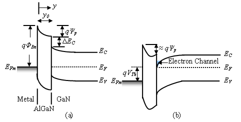 | Figure 3. Room temperature energy-band diagrams for a normally-off MODFET at (a) equilibrium and (b) onset of threshold |
 | (1) |
 | (2) |
 | (3) |
 Bn, Vth can be varied between positive and negative values. An example for a positive threshold voltage Vth is shown in Figure 4 and the transistor shows normally-off characteristics. Moreover, with a gate voltage larger than the threshold voltage the 2DEG sheet in the channel induced by the gate as a function of the distance x is capacitive coupled and is given by:
 | (4) |
 | (5) |
 | (6) |
 | (7) |
 | (8) |
 | (9) |
 | Figure 4. Output characteristics of an enhancement-mode MODFET |
 | (10) |
 | (11) |
 | (12) |
3. Results and Discussion
3.1. Variation in Thickness of Cubic GaN Buffer Layer
- In our calculations we use 3C-SiC (001) as the substrate for the cubic AlxGa1-xN/GaN MODFET structures. Figure 5 shows a schematic drawing of the structure of MODFETs (sample A). The thickness of the UID c-GaN buffer layer was varied in the calculations. The background n-type doping concentration in this layer is ND = 1 x 1017 cm-3. On top of GaN buffer a 4 nm UID cubic Al0.25Ga0.75N spacer layer with ND = 4 x 1017 cm-3, 6 nm cubic Al0.25Ga0.75N: Si with ND = 4 x 1018 cm-3 and 10 nm UID cubic Al0.25Ga0.75N with ND = 4 x 1017 cm-3 are placed. In addition, we use two-dimensional device simulator nextnano3 software[25] for numerical simulation of the electrical output and transfer characteristics. Our devices have a gate length of 2 µm and a source-to-drain spacing of 8 µm.
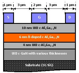 | Figure 5. Cross sectional view of cubic AlxGa1-xN/GaN based MODFETs (sample A) using for simulation |
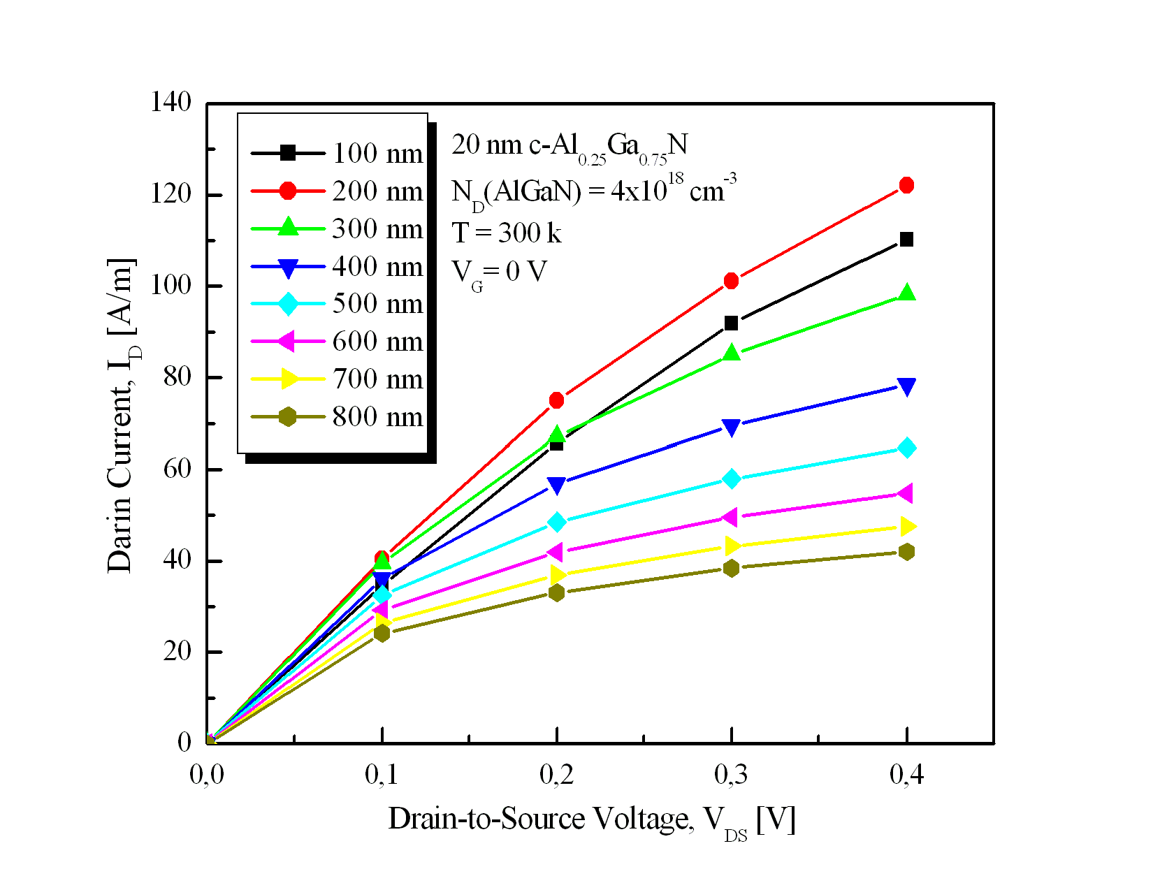 | Figure 6. Room temperature electrical output characteristics of cubic AlxGa1-xN/GaN MODFETs (sample A), calculated using nextnano3 devices simulation software, for different thickness of c-GaN buffer at VGS = 0 V |
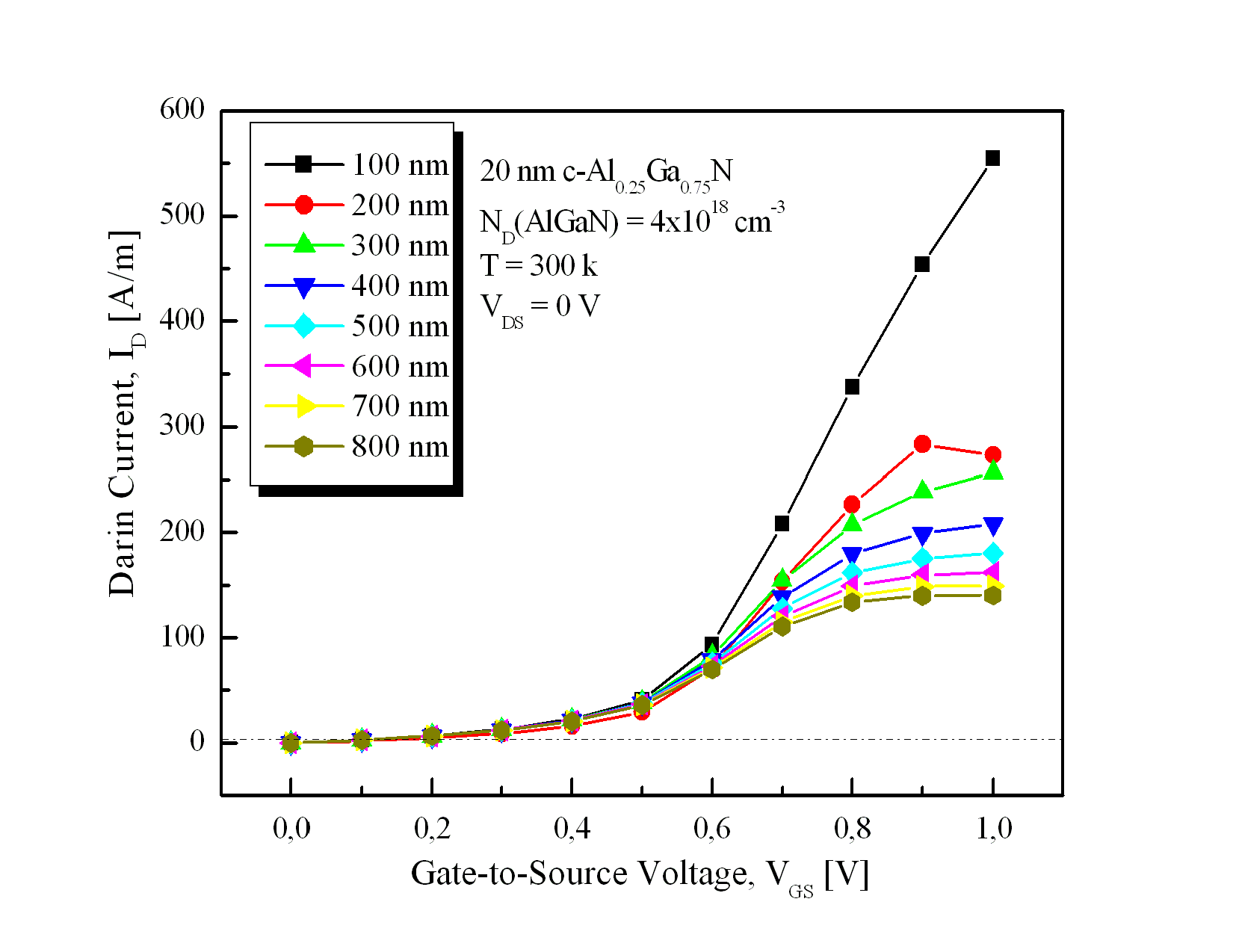 | Figure 7. Room temperature transfer characteristics of cubic AlxGa1-xN/GaN MODFETs (sample A), calculated using nextnano3 devices simulation software, for different thickness of c-GaN buffer at VDS = 0 V |
3.2. Variation in Donor Concentration Within the δ-doped Layer
- Figure 8 shows the structure of sample B consisting of 200 nm unintentionally doped (UID) cubic GaN buffer layer, 4 nm UID cubic Al0.25Ga0.75N spacer layer, 6 nm cubic Al0.25Ga0.75N: Si and 10 nm UID cubic Al0.25Ga0.75N.
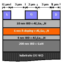 | Figure 8. Cross sectional view of cubic AlxGa1-xN/GaN based MODFETs (sample B) using for simulations |
 -doping, the maximum transconductance of MODFETs device depends on the maximum carrier sheet density in the channel at the AlxGa1-xN/GaN interface. The carriers in the electron channel are generally transferred from AlxGa1-xN barrier to the hetero-interface. Therefore, doping of AlxGa1-xN barrier is necessary to achieve high electron sheet concentration and therewith high device transconductance. The use of a
  -doped layer within AlxGa1-xN barrier placed close to the channel interface allows the local separation of electrons and donors to reduce impurity scattering and increase electron mobility within the channel.Calculations were performed with the described model to estimate an optimized
  -doping concentration within cubic Al0.25Ga0.75N barrier layer. Figure 9 shows transfer characteristics of cubic AlxGa1-xN/GaN MODFETs for different δ -doping levels. According to the calculated curves, all devices with
  -doped cubic AlxGa1-xN layers are fully depleted already at VDS = 0 V.Moreover, the drain-to-source current increases with increasing δ -doping level within the cubic Al0.25Ga0.75N layer, and therewith high device transconductance is achieved. The calculation of the electrical transfer characteristics visualize that intentional doping of cubic AlxGa1-xN barrier layer is essential to obtain high device transconductance. With the highest doping concentration of
  -layer, that is ND(δ) = 6 x 1018 cm-3, the device exhibits the highest drain saturation current as shown in Figure 10.These results show that to accomplish the modulation doping of the barrier layer it is necessary to use a δ -doped layer within AlxGa1-xN barrier, placed close to the channel interface, which allows the local separation of electrons and donors. This method allows a reduced impurity scattering and increases the electron mobility within the channel. The Schottky gate contact with a barrier height of 0.8 eV was localized on top of the cubic AlxGa1-xN layer. As in the realized MODFET devices[26], the gate length was 2 µm and the gate-to-source and gate-to-drain spacing was 3 µm. It was not possible to include the effect of gate leakage in the simulation.
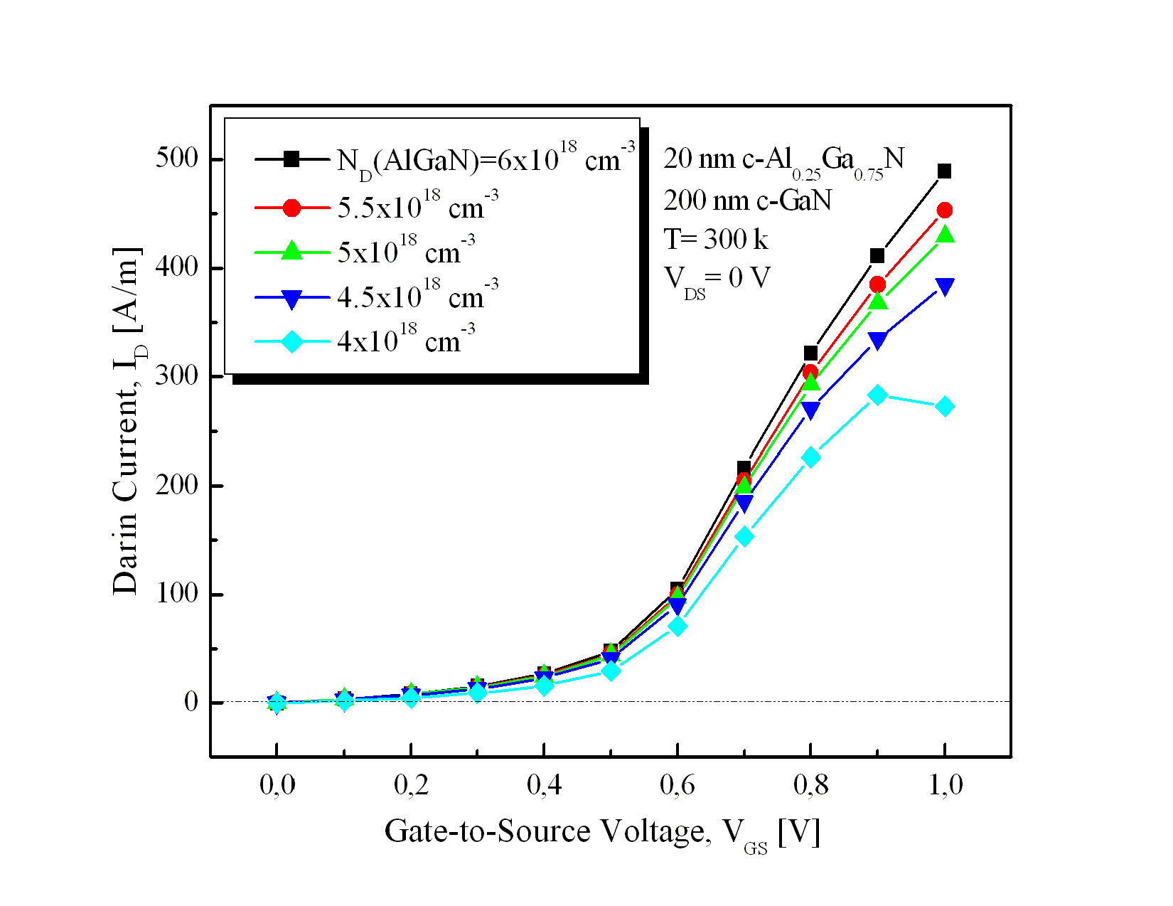 | Figure 9. Room temperature transfer characteristics of cubic AlxGa1-xN/GaN MODFETs (sample B),  -doping level varied within the Al0.25Ga0.75N barrier layer at VDS = 0 V -doping level varied within the Al0.25Ga0.75N barrier layer at VDS = 0 V |
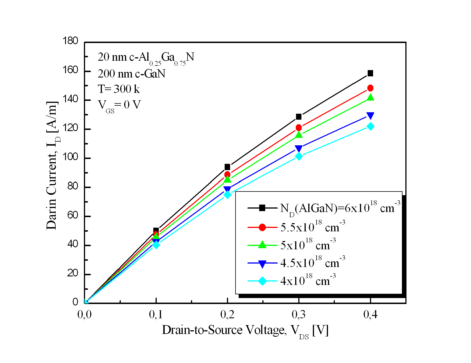 | Figure 10. Room temperature output characteristics of cubic AlxGa1-xN/GaN MODFETs (sample B), for different δ-doping AlxGa1-xN barrier layer at VGS = 0 V |
3.3. Simulation at Different Voltages
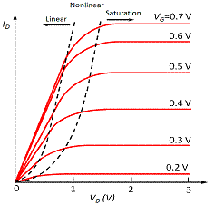
- Figure 11 shows the room temperature dc drain current voltage (I-V) curves of a cubic MODFETs device. A clear field-effect was calculated with this device when the gate-to-source voltage varied from -100 mV to +100 mV. The increase in the calculated drain current with increasing VG proves a good agreement with the normally-off MODFET devices. However, it is possible to include the effect of gate leakage in the simulations.Furthermore, the transfer characteristics of cubic MODFETs (sample B) were calculated with the two-dimensional device simulator nextnano3, for different drain-to-source voltages from -100 mV to +100 mV and are displayed in Figure 12. The threshold voltage of this device is +0.4 V at VDS = 0 V. This indicates normally-off device characteristics.
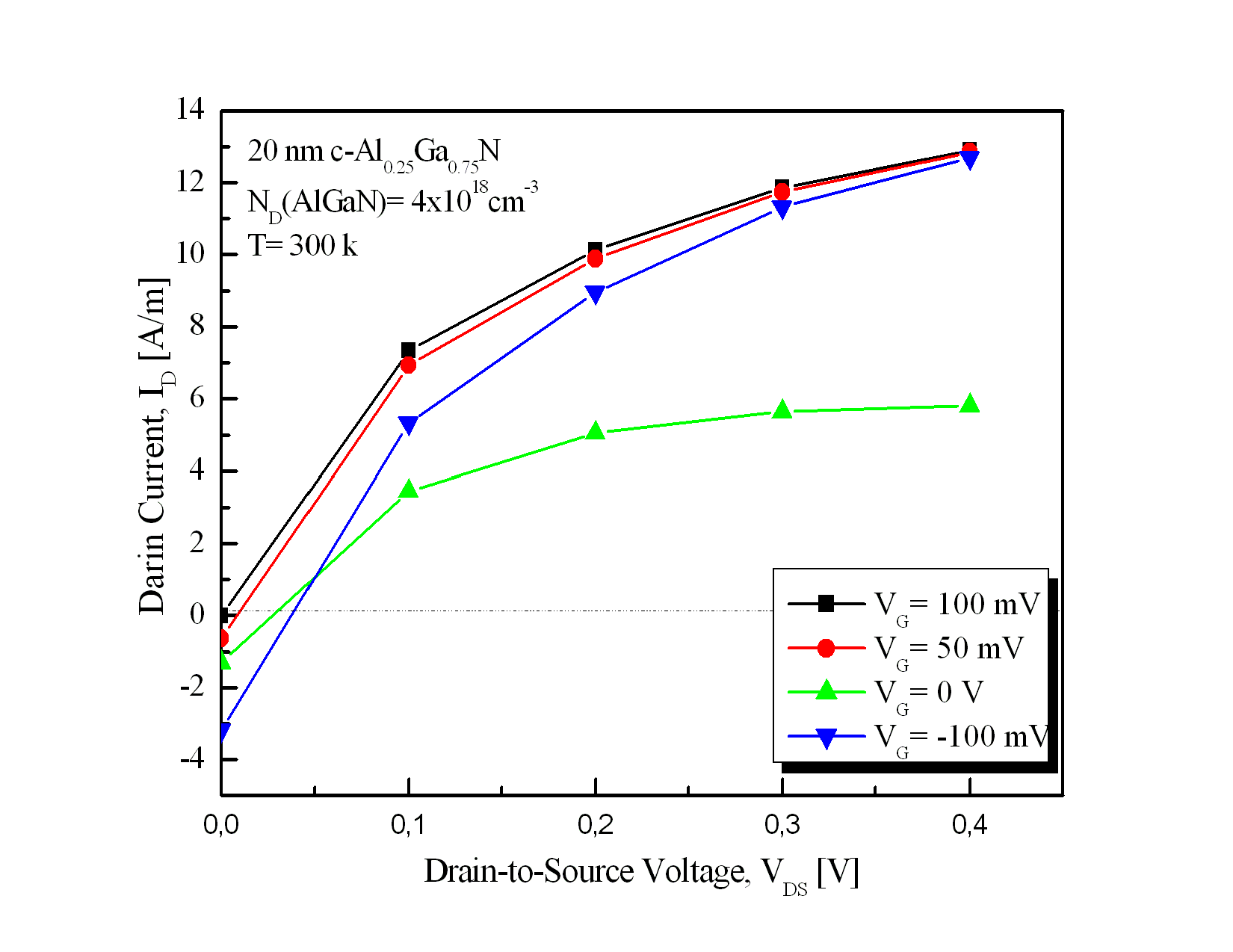 | Figure 11. Room temperature output characteristics of cubic AlxGa1-xN/GaN MODFET sample B, calculated using nextnano3 devices simulation software at VG = -0.1 V, 0 V, +50 mV, and +0.1 V |
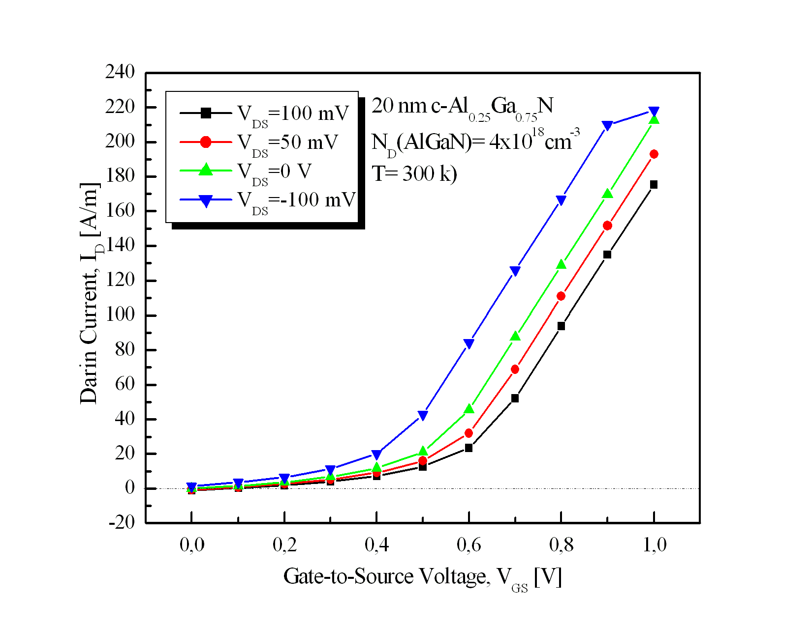 | Figure 12. Room temperature transfer characteristics of cubic AlxGa1-xN/GaN MODFETs (sample B), calculated using nextnano3 devices simulation software at VDS = -0.1 V, 0 V, +50 mV, and +0.1 V |
3.4. Variation in Al Content within the AlxGa1-xN barrier Layer
- Figure 13 shows calculations of the electrical output characteristics of a MODFET transistor, for different Al content x in the AlxGa1-xN barrier layer. Our results show that, for x = 25% the MODFET reaches the maximum drain source saturation current of IDSsat = 130 A/m compared with those obtained with x = 30%, 32% and 33%. The electrical transfer characteristics are shown in Figure 14, where the MODFET presents a low threshold voltage around 0.4 V for Al content x = 25%. The electrical output and transfer characteristics were calculated at VGS = 0 V and VDS = 0 V respectively. Results show that an improvement of the device transconductance and of the performance of normally-off MODFET devices can be reached by varying Al content in the AlxGa1-xN barrier layer.
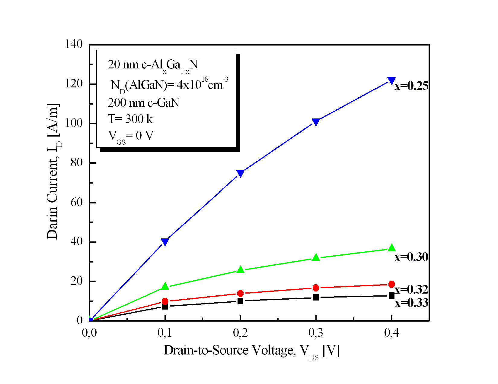 | Figure 13. Room temperature electrical output characteristics of cubic AlxGa1-xN/GaN MODFETs (sample B), calculated using nextnano3 devices simulation software, for different Al contents |
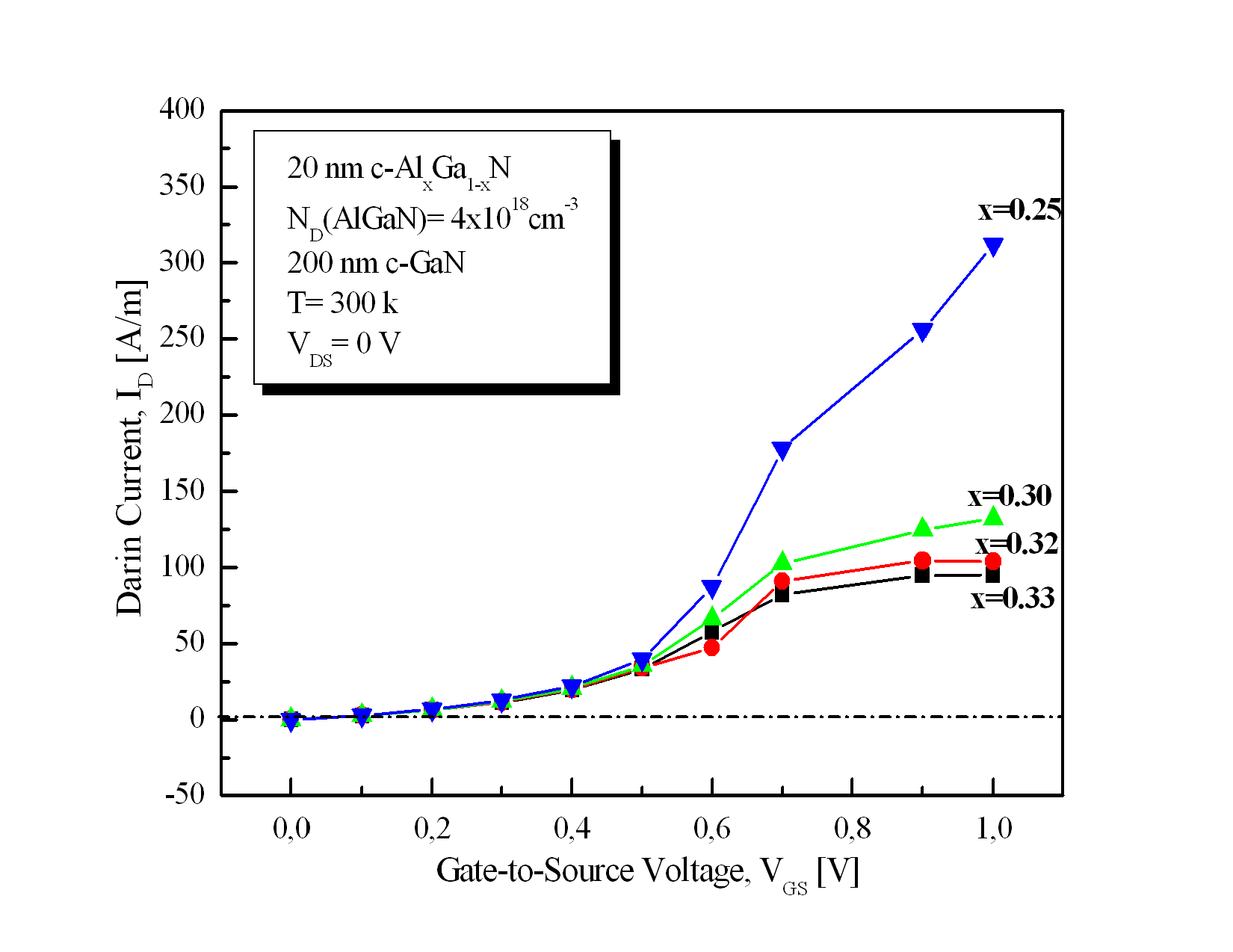 | Figure 14. Room temperature electrical transfer characteristics of cubic AlxGa1-xN/GaN MODFETs (sample B), calculated using nextnano3 devices simulation software, for different Al contents |
4. Conclusions
- The main focus of this work is the simulations results of the output and transfer characteristics of cubic AlxGa1-xN/GaN based MODFETs structures, by using samples with a different thickness of cubic GaN buffer layer and with different δ - doping and different Al contents. Our results show a clear field-effect at positive bias voltages with Vth = 0.4 V. However, due to the gate leakage the device has not yet exhibited the characteristics of an ideal normally-off FET. On one hand, our results of simulations demonstrate clearly that cubic Al0.25Ga0.75N/GaN can be used for the MODFETs with normally-off mode operation behavior. On the other hand, simulation of the output characteristics is in good agreement with the finding that the shunt current is mainly due to the gate leakage. In addition, we find the highest values of drain source saturation current for a device with 100 nm of buffer layer, ND(δ) = 5.5 x 1018 cm-3 or around ND( δ ) = 6 x 1018 cm-3, and Al content of the barrier layer x =25%, at VGS = 100 mV. For this structure, the transfer characteristics show a low threshold voltage value and the highest maximum transconductance gm, among the simulated MODFET structures.
ACKNOWLEDGMENTS
- The work is a joint collaboration between the group of Physics and Technology of Optoelectronic Semiconductors at University of Paderborn, Germany and Laboratory of Electrical Engineering at University of Sciences and Technology of Oran, Algeria.