-
Paper Information
- Next Paper
- Previous Paper
- Paper Submission
-
Journal Information
- About This Journal
- Editorial Board
- Current Issue
- Archive
- Author Guidelines
- Contact Us
Electrical and Electronic Engineering
p-ISSN: 2162-9455 e-ISSN: 2162-8459
2012; 2(5): 303-308
doi: 10.5923/j.eee.20120205.10
For the Journal “Electrical and Electronic Engineering”, SAPUB Design of PCB for Power LEDs – Thermal Investigations
 Abstract
 Reference
 Full-Text PDF
 Full-Text HTML
Petko Mashkov , Berkant Gyoch , Stanislav Penchev , Hristo Beloev
Studentska str., University of Ruse, Ruse, 7017, Bulgaria
Correspondence to: Petko Mashkov , Studentska str., University of Ruse, Ruse, 7017, Bulgaria.
| Email: |  |
Copyright © 2012 Scientific & Academic Publishing. All Rights Reserved.
Investigations deal with development of cost effective thermal management for power LEDs. The technique involves usage of FR4 based PCBs which cost less, but have greater thermal resistance than metal core printed circuit boards (MCPCB). The use of copper pins underneath LED thermal pad is a method to dissipate heat through an FR4 PCB into an appropriate heat sink. Temperature regimes of operation of power XLamps LEDs mounted on MCPCBs and on the PCBs with copper pin are experimentally tested at various ambient conditions (air temperatures from 20℃ to 45℃) and different current values through LEDs – up to 600 mA. Infrared thermography for evaluation of temperature distribution on LEDs and heat sink is used. Thermal management investigations show that the developed design of FR4 PCB is successful and possess a lot of advantages.
Keywords: Power Leds, Leds’ Thermal Management
Cite this paper: Petko Mashkov , Berkant Gyoch , Stanislav Penchev , Hristo Beloev , "For the Journal “Electrical and Electronic Engineering”, SAPUB Design of PCB for Power LEDs – Thermal Investigations", Electrical and Electronic Engineering, Vol. 2 No. 5, 2012, pp. 303-308. doi: 10.5923/j.eee.20120205.10.
1. Introduction
- Power LEDs possess a lot of advantages in comparison to other light sources. Luminaire efficacy of LEDs is better than efficacy of CFL (Compact Fluorescent Lamps) more than two times; LEDs’ lifetime is five to fifty times longer than CFL’s lifetime before requiring maintenance, there’s no mercury, less power – plant pollution, less handful waste. But realizing advantages of LED luminaire demands precise thermal management calculations and investigations. It is well known that during operation of LEDs about 85% of electric power is turned into a heat in the LED chip and one of the most critical design parameters in LED illumination systems is the system’s ability to draw heat away from the LED junction[1 – 3]. High operating temperatures at the LED junction adversely affect the performance of LEDs, resulting in decreased light output and lifetime. The parameters which influence strongly on the junction temperature are: ambient temperature of the LED’s immediate surroundings; power dissipated by the LED and thermal path between the LED junction and surroundings. The designer can not influence on the ambient temperature; the LED’s power depends on the desirable luminous flux of one LED and in practice the most important task for realization all benefits of LED luminaire is proper thermal management of lighting equipment. Proper thermal management has to be considered in all its aspects. On one hand thermal resistance between solder point and immediate surroundings must be as low as it is possible; on the other hand assembling of LEDs onto the heat sink has to be easy, with few manual operations and cost effective.The purpose of the investigations is designing a low-cost printed circuit board (PCB) layout which optimizes the transfer of heat from the LED.
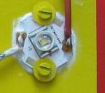 | Figure 1. XLamp LED (XR-E) mounted on MCPCB |
2. Problem Statement
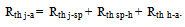
- Light equipment is designed on the base of LEDs XLamp XR – E White, CREE Inc., with light output 100 lm at 350 mA. At unconditioned spaces maximum ambient temperatures can reach 45℃ and proper heat sink must be chosen. During operation heat flows from junction of the LED via solder point, PCB to the heat sink by way of conduction. The heat sink diffuses heat to the ambient surroundings mostly by convection[1]. Thermal resistance between junction of LED and ambient is a sum of thermal resistances:- from the junction to the solder point (Rth j-sp);- from the solder point to the heat sink (Rth sp-h);- from the heat sink to ambient (Rth h-a)[1]:
 | (1) |
 | Figure 2. Thermal resistance model for 12 XLamps LEDs. Rth j-sp- thermal resistance from junction to solder point; Rth sp-h- thermal resistance from solder point to heat sink; Rth h-a- thermal resistance from heat sink to ambient |
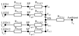
 | Figure 3. FR4 cross-sectional geometry. HASL - Hot Air Solder Level |
 | Figure 4. MCPCB cross-sectional geometry |
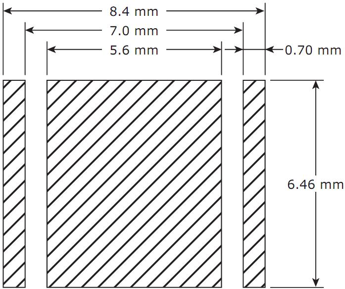 | Figure 5. Recommended solder pad for XLamp XR family LEDs |
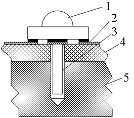 | Figure 6. LED soldered on FR4 PCB with copper pin; 1 – LED; 2 – copper layer; 3 – copper pin; 4 – FR4 PCB; 5 – heat sink |
3. Results
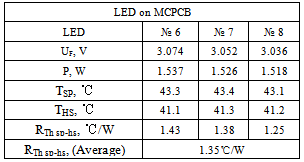
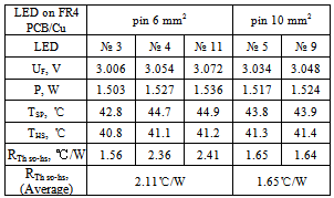
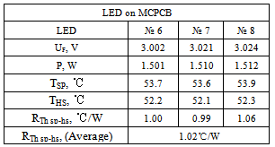
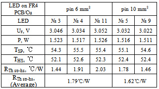
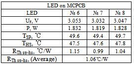
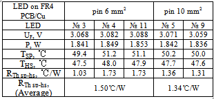
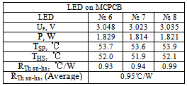
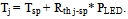
- For evaluation of thermal effectiveness of PCB with copper pin (Fig. 6) a proved measuring method which is well described in[4, 5] is applied. LED panel is placed in experimental thermo chamber– Fig. 7. Infrared thermography is used for obtaining real temperatures of solder points of LEDs and temperature distribution on the heat sink’s surface at different regimes of operation and different ambient conditions. Temperature distribution measurements are carried out using IR camera ThermaCam E300 – FLIR-Systems as it is described in[4, 5]. Results are verified by conventional measurements (by thermocouples mounted on two LEDs) in a manner recommended in[1].Temperature in the thermal chamber is changed from 20℃ to 45℃ at intervals of 5℃. The value of current through LEDs is changed from 350 mA to 600 mA at intervals of 50mA. At each temperature and value of forward current when temperature equilibrium in the chamber is achieved, photos by IR camera are made. At each temperature the forward voltage drop on every LED is measured and real power consumption of every LED is calculated. Voltage measurements are carried out using multi meter MS-8050 with accuracy of 0.03%.
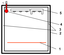 | Figure 7. Cross-section view of experimental thermo chamber: 1- heater; 2- corpus of the chamber; 3- thermal insulation; 4- thermometer; 5 – LEDs panels |
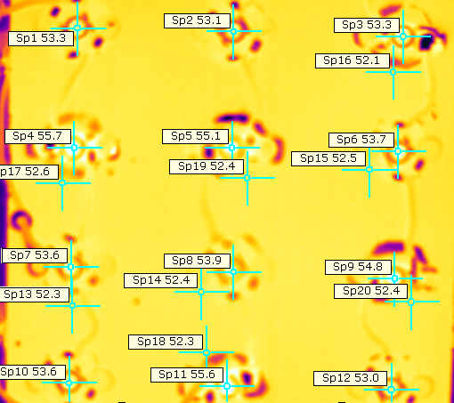 | Figure 8. Photo of the LEDs’ panel made by IR camera; Ta = 40℃ ; IF = 350 mA – forward current through LEDs |
 | (2) |
 | (3) |
|
|
|
|
|
|
|
|
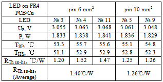
 | (4) |
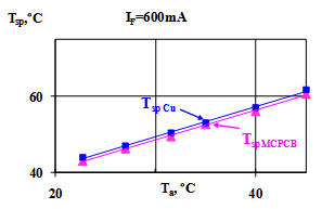 | Figure 9. Solder point’s temperature Tsp dependences on temperature of the ambient air Ta; IF = 600 mA – forward current through LEDs. Tsp-Cu – for LEDs on FR4 PCBs with 6 mm2 copper pin (■); Tsp-MCPCB – for LEDs on MCPCBs (▲) |
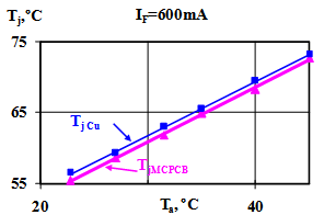 | Figure 10. Junction temperature Tj dependences on temperature of the ambient air Ta; IF = 600 mA – forward current through LEDs; Tj-Cu – for LEDs on FR4 PCBs with 6 mm2 copper pin (■); Tj-MCPCB – for LEDs on MCPCBs (▲) |
4. Conclusions
- Design of low-cost FR4 printed circuit board (PCB) layout which optimizes the transfer of heat from LEDs to heat sink is proposed. Developed thermal performance of FR4 PCB includes usage of copper pins underneath LEDs’ thermal pads. This design ensures low thermal resistance between LED’s solder point and heat sink (like MCPCB) and gives possibility for realization easy, low cost, with few manual operations assembling of LEDs to the heat sink.
ACKNOWLEDGEMENTS
- This work was supported by the Ministry of Education and Science of Bulgaria under Grant Projects VU-EES-301/2007, 12-FEEA-02.