-
Paper Information
- Next Paper
- Previous Paper
- Paper Submission
-
Journal Information
- About This Journal
- Editorial Board
- Current Issue
- Archive
- Author Guidelines
- Contact Us
Electrical and Electronic Engineering
p-ISSN: 2162-9455 e-ISSN: 2162-8459
2012; 2(3): 135-140
doi: 10.5923/j.eee.20120203.05
Out-Band Interference Rejection in UWB LNA Receiver Using Coupled Inductors in Front End LNA
 Abstract
 Reference
 Full-Text PDF
 Full-Text HTML
Hossein Rezaei, Ebrahim Abiri, Mohammad Reza Sal
Department of Electrical and Electronics Engineering, Shiraz University of Technology, Shiraz, Iran
Correspondence to: Hossein Rezaei, Department of Electrical and Electronics Engineering, Shiraz University of Technology, Shiraz, Iran.
| Email: |  |
Copyright © 2012 Scientific & Academic Publishing. All Rights Reserved.
In this paper, an ultra wide band (UWB) low noise amplifier (LNA) circuit with a new input stage is proposed. In this scheme, a combination of coupled inductors in the input stage is utilized. The input stage is able to easily reject out-band interference. This input stage is applied in an LNA with 0.18 μm technology. The LNA has a peak gain of 21.72 dB in 3.1-10.6 GHz frequency band while showing a minimum noise figure of 1.85 dB in the mentioned frequency band. This circuit rejects 15.2 dB out-band interference, while power consumption of the UWB LNA core is 11.8 mW DC which is supplied from a 1.8 V power supply. s11 is less than -10.3 dB over the entire bandwidth since the worst value of IIP3 over the entire bandwidth is -13 dBm, which occurs at the frequency of 10.6 GHz.
Keywords: Out-Band Interference, Ultra Wide Band (UWB), Low Noise Amplifier (LNA), Coupled Inductors
Article Outline
1. Introduction
- UWB standard was proposed by the federal communication committee (FCC)[1] in frequency range of 3.1-10.6 GHz. Due to the wide frequency band, UWB systems are capable of increasing the transmission rate up to 450 Mbps[2, 3]. Therefore, UWB systems are widely used for numerous applications in the form of WPAN[4] and short- range wireless communications[5, 6].One of the major challenges associated with these systems is the presence of interferer signals in the mentioned frequency range which can cause destructive effects on received UWB signal. Interferer signals can be classified into two general categories. The first category mainly causes in-band interference and is a result of WLAN systems which works under IEEE 802.11a standard and takes in the frequency range of 5-6 GHz. The other category is related to WLAN systems working under IEEE 802.11 b/g standard. This kind of interference is called out-band interference, due to occupying the frequency band of 2.4-2.48 GHz. The high power interference signal caused by these systems may saturate the UWB LNA receivers and consequently degrade the sensitivity of the system. Thus, removing this type of interference is considered as a crucial issue in designing RF transceivers. As a result, the performance of UWB transceivers can be guaranteed by more than 15 dB rejection.Lots of attempts have been carried out to improve the system performance which led to proposing various techniques. Gm-boosting[7] and thermal noise cancellation fordecreasing the noise figure[8, 9], current reuse topology to perform UWB input matching and cascade amplifier with resonant load to enhance gain and reverse isolation [10], the bridged-shunt-series peaking technique for increasing the bandwidth and improving the matching in the output[11] are some of the generic methods mentioned in the literature. Although improving system performance, these methods are not capable of interference rejection. Recently, various methods have been proposed for interference rejection mostly designed using notch filters[12-15]. These filters are able to be tuned over the rejected frequency. However, because of using an additional circuit for rejecting the considered frequency, these filters will cause an increase in the power consumption and noise figure.In this paper, we aim to reject out-band interferer signals in the input stage in such a way that there will be no increase in power consumption and no effect on the noise figure. Also, powerful tuning over the considered frequency will be preserved. Here, it is possible to increase the signal power in the next stages in an appropriate manner so that the presence of interferer signals will not be considerable.The proposed circuit as an input stage has a maximum noise figure of 0.42 dB in the frequency range of 3.1-10.6 GHz. For both mentioned frequency bands, s11 and s22 are below -12 dB and -10 dB, respectively. The minimum gain value over the mentioned frequency band for the circuit is -0.76 dB, while the power consumption is zero, and hence CS LNA is added to the input stage to improve the gain. In order to compensate the NF of the circuit, the advantages of thermal noise cancellation techniques have been used in the second stage[8]. Furthermore, in order to improve the gain and input matching of the circuit in higher frequencies, a new innovating technique is employed based on the bridged-shunt-series peaking method[11] in the output buffer using monolithic transformers[16].The rest of this paper is organized as follows. In section 2, the overall circuit design, initially proposed input stage, CS LNA and output buffer with the innovative technique are presented. Simulation results are given in section 3. Finally, we will conclude the paper in section 4.
2. Circuit Design
2.1. Input Stage
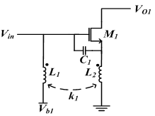
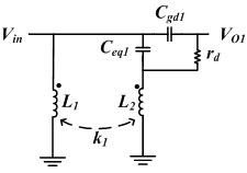
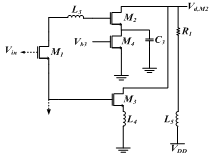
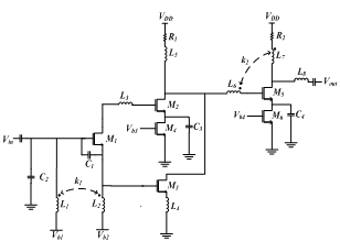
- The proposed input stage is shown in Figure 1. In this circuit, combination of coupled inductors with M1 rejects out-band interference. Small signal equivalent circuit is shown in Figure 2.
 | Figure 1. Schematic of the proposed interference rejection circuit |
 | Figure 2. Small circuit equivalent of the interference rejection circuit |
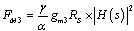
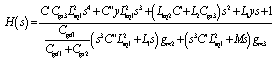
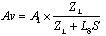
 , hence, power gain can be derived as:
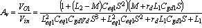 | (1) |
 ,
, and also
 . From (1), it can be deduced that there is one frequency, f, which leads gain of circuit to zero. This frequency is given in (2). Hence, the out-band interference can be rejected by tuning f on 2.4 GHz.
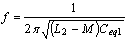 | (2) |
2.2. CS LNA
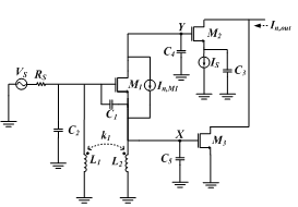
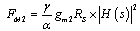
- In this design, the procedure of designing UWB LNA with interference rejection consists of three steps. First, as described previously, in order to reject any arbitrary frequency, the best parameter of (2) should be selected. Second, CS LNA and output buffer are added to the circuit. Third, by selecting the best value of other circuit parameters, NF, s11, and s22 can be optimized.Gain deficiency is the reason for designing the next stage as an amplifier. For this purpose as shown in Figure 5, CS LNA with thermal noise cancelation technique has been applied. The concept of noise cancellation can be extended as[8, 9].
 | Figure 3. a. The gain and NF b. s11 and s22 of the circuit |
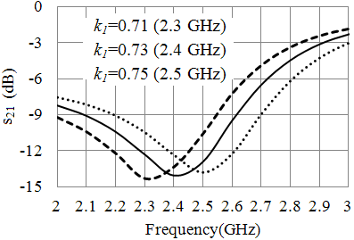 | Figure 4. NF with variation of k1 |
 | Figure 5. Schematic design of noise cancelation technique |
 | (3) |
 | (4) |
 | (5) |
 ,
, ,
, ,
, ,
,
 | Figure 6. Schematic design of the second stage in the proposed LNA |
 is a noise parameter,
  at which gd0 is the channel conductance for VDS=0. As shown, by increasing gm2 to be more than gm3, the noise factor of M2 and M3 can be decreased. Furthermore, increasing gm2 in an excessive manner can ruin power gain and NF, hence Id,M2=4.87 mA and Id,M3=1.69 mA are selected. As shown in Figure 5, C2 increases the amount of Cgd1 which improves input matching at high frequencies. On the other hand, in order to improve input matching of the circuit in high-band frequency,
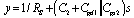
  has been used at which ωU is the upper cut-off frequency and R (50Ω) is characteristic impedance at both ports. As shown in Figure 6, the bandwidth extension of LNA can be obtained using inductance L5 without any high Q requirement[17]. As shown, M4 with gate bias provides the DC current path of M2, since C3 provides ac ground of circuit over working frequency bands. Resonating L3 with input parasitic capacitance of M2, improve input matching and gain at high frequencies.
2.3. Output Buffer
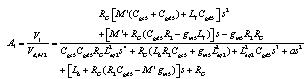
- Combination of inductance L7 and L8 with the series inductance L6 results in the bridged-shunt series peaking network, which further extends the bandwidth and as a consequence gain flatness will be achieved (Figure 7)[11]. It is possible to increase the signal power by using positive feedback in this scheme.The positive gain between drain and gate can also be implemented through the use of on-chip transformer[7]. A monolithic transformer comprises two square spiral inductors. Furthermore, this transformer occupies less die area and provides a higher quality factor than two independent inductors[16]. Voltage gain in Figure 7 can be expressed as (6). A1 can be derived as illustrated in (7).
 | (6) |
 ,
,  and
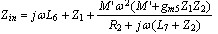
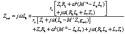
and  . Input and output impedances are derived as in (8) and (9), respectively, where
 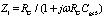 and
and  .Considering (7), (8) and (9), it is obvious that coupling between L6 and L7 can significantly affect gain, input, and output reflection coefficients of LNA. Furthermore, these effects should be considered on the proposed LNA.
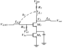 | Figure 7. Schematic design of the output buffer with coupling between L1 and L2 |
 | (7) |
 | (8) |
 | (9) |
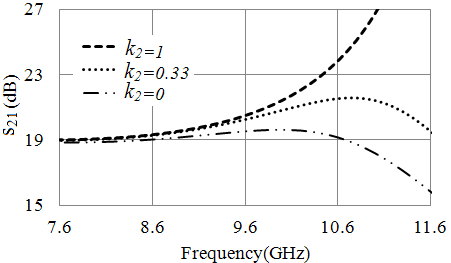 | Figure 8. The power gain versus k2 |
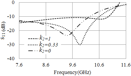 | Figure 9. The input reflection coefficient versus k2 |
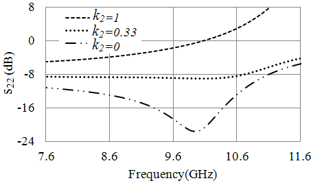 | Figure 10. The output reflection coefficient versus k2 |
3. Simulation Results
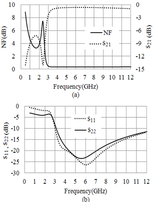
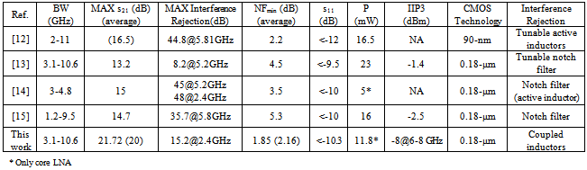
- The proposed three stage UWB LNA is shown in Figure 11. The circuit has been designed with TSMC 0.18 μm CMOS technology. The simulation results are obtained using Agilent ADS 2008A simulator. All inductors are spiral with low quality factor due to high series resistances. The, first, second and third stages as an output buffer draw 0, 6.55, and 4.42 mA, respectively, from a 1.8 V power supply. Consequently, the total power consumption is 19.76 mW. Figure 12 shows the simulated noise figure of the LNA, which varies from 1.85 dB to 3.33 dB, and also has an average amount of 2.16 dB over 3.1-10.6 GHz. As shown, the variation of the circuit gain over the mentioned frequency range will be from 19 dB to 21.72 dB. Also, the average amount of power gain is 20 dB. As can be observed, 15.2 dB rejection at 2.4 GHz compared to the maximum gain is obtained. Input reflection coefficient is shown in Figure 13, which varies from -27.5 dB to the worst case of -10.3 dB. This figure also shows reverse isolation which is less than -26.5 dB over the entire working bandwidth. Output reflection coefficient (s22) varies from -10 dB to the worst value of -7 dB over the mentioned frequency band. Another parameter which should be considered is group delay since a large amount of it may distort the signal phase. In our circuit, variation of group delay ranges from 77.3 ps to 329 ps over the frequency band which is acceptable[18]. The stability factor of the proposed circuit is more than one, so UWB LNA is always stable. By applying two tones with 1 MHz spacing, the simulated IIP3 is -10.5±2.5 dBm over the mentioned frequency bandwidth.Table 1 summarizes the performance of the recently reported UWB LNA with interference rejection using 0.18 μm CMOS technology. It is obvious that this design has the lowest amount of noise figure and the highest gain. In addition, more robust out-band interference rejection is achieved compared to the recently published CMOS LNA.
|
 | Figure 11. Circuit diagram of the proposed UWB LNA |
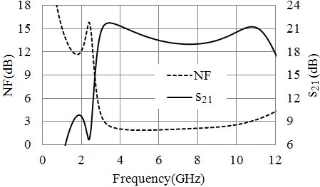 | Figure 12. NF and gain of the circuit |
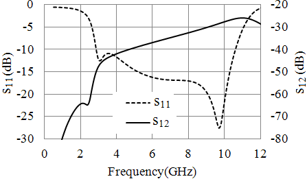 | Figure 13. The input matching parameter and the reverse isolation |
4. Conclusions
- Interference is considered as the main challenge in the UWB LNA receivers. In order to eliminate interferences, a new technique is introduced based on coupled inductors with confident rejection of out-band interference.Robust tuning, low noise figure and also no DC power consumption are obtained using this technique. A UWB LNA with this technique in first stage was designed. Advantages of CS LNA as an amplifier with thermal noise cancelation technique are used in the second stage of UWB LNA. Finally, output buffer is implemented with the bridged-shunt-series peaking technique to extend the bandwidth. This scheme using the innovative technique aims to improve the gain of the circuit at high frequency band. In comparison to other related conventional published methods, the proposed UWB LNA exhibits the lowest noise figure over a 3.1-10.6 GHz bandwidth with the highest average power gain for UWB application in a commercial CMOS process.
ACKNOWLEDGEMENTS
- The authors would like to thank Seyyed Ahmad Safaei for fruitful discussions and for providing technical guidance, also the National Iranian Gas Company (NIGC) for financial and technical supports.