-
Paper Information
- Next Paper
- Previous Paper
- Paper Submission
-
Journal Information
- About This Journal
- Editorial Board
- Current Issue
- Archive
- Author Guidelines
- Contact Us
Electrical and Electronic Engineering
p-ISSN: 2162-9455 e-ISSN: 2162-8459
2012; 2(3): 121-127
doi: 10.5923/j.eee.20120203.03
High Speed 16×16-bit Low-Latency Pipelined Booth Multiplier
Habib Ghasemizadeh, Amir Fathi, Akbar Ghasemizadeh
Department of Electrical Engineering, Salmas Branch, Islamic Azad University, Salmas, Iran
Correspondence to: Habib Ghasemizadeh, Department of Electrical Engineering, Salmas Branch, Islamic Azad University, Salmas, Iran.
| Email: |  |
Copyright © 2012 Scientific & Academic Publishing. All Rights Reserved.
This paper presents a high-speed 16×16-bit CMOS pipelined booth multiplier. Actually in an n-bit modified Booth multiplier, because of the last sign bit, n/2 +1 partial product rows are generated rather than n/2. The extra row not only increases the delay and power consumption of Wallace tree, but also it leads to irregularity and complexity of Wallace tree designing. In this multiplier the last sign bit is removed by using a simple high-speed approach. This causes 4% reduction in power consumption and 5.2% reduction in transistor count. Also by using new partial product generation and booth encoder circuits and a novel adder, speed of pipelined multipliers is improved. By these new architectures, final adder performs 25 bit addition in only two cycles with high speed (1.6 GHz). Due to lower number of cycles (5 clock cycles), delay of the overall circuit is only 3.1ns and besides power consumption is decreased so that at a data rate of 1 GHz and under the supply voltage of 3.3V, power consumption is 169mW. This multiplier is implemented in TSMC 0.35µm CMOS technology.
Keywords: Carry-Select Adder, Carry-Lookahead Adder, Multiplier, Modified Booth Algorithm, Partial Products, Pipeline
Article Outline
1. Introduction
- Increasingly demand for high speed data processing motivated researchers to seek faster processors. Multiplier as one of the building blocks of processor has a great impact on the speed of processor, and hence high speed multipliers are under active research. Resent high speed parallel multipliers contain three sections: first part is partial product generation and a common approach for performing it is using Modified Booth Encoding (MBE) approach, Because this multiplication is signed multiplication and besides the number of rows in a n-bit multiplier are decreased to n/2 +1[1–8] rows. In the Second part partial products reduction schemes, such as Wallace trees or compressor trees are used for adding partial products vertically until, rows that were generated in part one decrease to two rows (sums and carries)[4,5]. Finally, third section is final adder that must adds two rows generated in part two, this part uses some kind of advanced adder approach such as carry-look ahead[2,10] or carry-select adders[4,5].Any improve in each section leads to improvement in the multiplier performance. Furthermore, pipeline technique could be used for raising the speed of multiplier. But due to increasing of stages (and hence number of clock cycles) latency, high power consumption and large area are draw tecture of the proposed pipeline multiplier. backs of pipelined systems. Fig.1 depicts the overall archi.By using new MBE circuit and novel hybrid adder topology, not only delay of stages is decreased, but also number of cycles is reduced (Only 5 cycles), hence speed of the circuit is improved. Besides because the number of cycles is decreased, number of devices and so power consumption and die area are decreased.
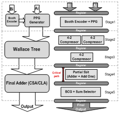 | Figure 1. Block diagram of the proposed pipelined multiplier |
2. New MBE Partial Product Generation
- In a n-bit modified Booth multiplier number of required Booth encoders is n/2 and the number of partial product generation (PPG) circuits is approximately n2, hence power consumption and die area in the Booth section is dominated by PPG and so integration of PPG section is more important than Booth encoder (BE) block. The conventionally used modified Booth selector computes the j-th partial product bit in the i-th row (PPi,j) according to the equation 1:
 | (1) |
 | (2) |
|
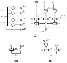 | Figure 2. Proposed MBE: (a) Booth encoder and selector (PPG), (b) Proposed circuits to generate Ki and (c) Hi |
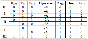
 b2i-1 is equal to one (equivalent to multiply by one), and middle branch of PPG conducts. in area II, Twoi
  =1 where Yi = b2i
  b2i+1 (equivalent to multiplied by two), in this case right branch of PPG conducts and shifts the data to left side, and in area III, both Xi and Yi are zero (equivalent to multiplied by zero), and left branch handles sign’s bit (b2i+1) to the output. In two’s complement operation, sign bit
  of each row must be added with that row. Hence this sign bit of last row cause to have 9 bit column. For having same delay for all branches, size of middle transmission gate is smaller (half) than other transmission gates. Besides by separating NMOS and PMOS devices and merging similar transistors in layout, higher speed is achievable.Function of sign changing in most of PPG circuits is performed by XOR gate, but in the proposed PPG a XNOR gate and an inverter in the output realize this function, and low driving capability of transmission gates is overcame by output inverter. Fig.3 shows well arranged structure of Wang[7] that was used in this work, but by this difference that in our structure, we didn’t use extra row omitting method of[6] and[7], because latency of omission of additional row is large and is useless in our high speed pipeline structure (table.2). In this multiplier the last sign bit (Negi) is removed by using a simple high-speed approach described in detail in the following section. Furthermore, the logic equations of Ki and Hi in Fig.3 can be derived as:
  | (3) |
 | (4) |
3. Extra Partial Product Row Removing
- As mentioned, in Booth algorithm, the sign bit of each array (Negi=B2i+1) is added to each partial product row[6]. Doing so completes 2-complement in Booth algorithm. Addition of sign bit in the last array is same as adding an extra row to partial product rows. Generally, in an n-bit Booth multiplier, n/2 +1 partial product row will be generated. The extra row, not only increases the delay and power consumption of Wallace tree[6, 7], but it also leads to irregularity and complexity of Wallace tree designing. For example, in a 16-bit multiplier which uses compressor for reducing partial products, the extra row necessitates using eight 5-2 compressors. Whereas, in the absence of such redundant row, the whole multiplier could have functioned merely with 4-2 compressor (which is both smaller and faster[12]) as well as having a more convenient design and arrangement. This fact is more prominent in bigger multipliers since in which due to a bigger hardware, the repeating trend of blocks will affect greatly on ease of connections in layout and consequently,
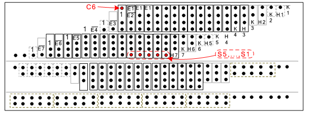 | Figure 3. Architecture of proposed partial products after removing the last sign bit |
4. Compression Module
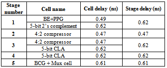
- Among different methods and circuits that are used for adding bits by same value in a column, using parallel compressors, due to its higher speed and low area, is more usual[4,5,12]. As depicted by fig.3, eight complete rows are generated by first stage; hence we have eight rows that must be added and reduced to two rows until final adder adds these two rows and compute the last result. As is obvious from fig.1, this function is performed in second and third cycles. In the second cycle two rows of 4:2 compressors convert 8 rows to 4 rows simultaneously, so after second stage 4 rows remains. In the third cycle one row of 4:2 compressors reduce row’s number from 4 rows to 2 rows. In other Columns, depend on the situation; we used 3:2 compressors or half adder, such that less area and power be consumed. This procedure is applied to the second stage as well (fig.3). On the other hand, because simultaneous arriving of data is important in pipeline structures, we used inverters for latency matching between columns. Besides, as is depicted in fig.3 in the third stage, from column 3 to column 7, two rows exist and hence these two rows could be decreased to one row by a high speed five bits adder. Two clear advantages of this reduction is: first, for data transmission only five flip-flops are needed (rather than ten flip-flops), second and more important, final addition is reduced to 25 bits (rather than 30 bits) and so, we could achieve to response more rapidly.
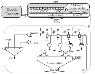 | Figure 4. Finding two’s complement conversion signals for five bits |
5. Novel Final Adder
- Among different adders, carry select adder (CSA) is known as a moderate adder, with respect to speed and die area[14]. But, some attempts were performed to improve these characteristics. For example, in[13], by the aid of an add-one circuit die area reduced by 29.2%. Also,[15, 16] by combining CLA and CSA improved speed. For the final adder, we combined these two schemes and applied changes such that the proposed structure to be compatible with pipeline structure. Fig.5 shows this adder that is realized in two cycles.
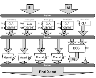 | Figure 5. Block diagram of the proposed pipelined final adder |
 | (5) |
 | (6) |
 B1 settles, half adder generates one bit, so in a determined time, we could add an additional bit.
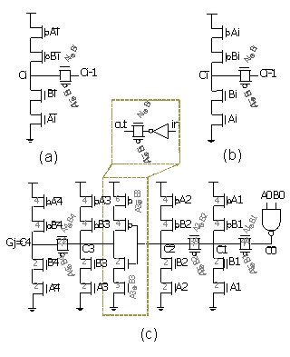 | Figure 6. Proposed CLA circuit: (a) generator cell, (b) generator cell (c) 5 bit CLA. |
 Bi rather than adder outputs (Si,j), because in partial adders, Cin=0 and Sis are one until Ai
 Bi is one. And first Sk=0 occurs when Ak
 Bk=0. After occurrence of first zero, outputs of add-one circuit become one for bit number k and later bits[15].
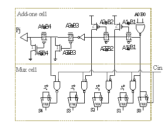 | Figure 7. Used add-one and sum selection cell |
 | (7) |
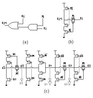 | Figure 8. Proposed BCG: (a) gate level (b)1 bit Block Carry Generator (c)5 bit Block Carry Generator |

 , all multiplicands must be one, in another word, all Ai.Bi products must be zero. Since in partial adder Cin=0, so final carry out, Gj, will be zero. Now we can use circuit of fig.8 (b) instead of fig.8 (a) because it has one TG delay. As Pj.Gj=0, hence we have three situations. First Gj=1 and Pj=0, in this case TG and NMOS branches are off, but PMOS branch conducts and output will be one. Second, Gj=0 and Pj=0, in this situation TG and PMOS branches are off, but NMOS branch conducts and output will be zero,. In the third case Gj=0 and Pj=1, vertical branches are off and TG conducts. Fig.8 shows Block Carry Generator, that uses one inverter and supplement circuit similar to CLA. Because each output of BCG circuit is input carry (Cin) of a five bit block, hence gate capacitances in the output passes of BCG is large and could impact the speed considerably. For overcoming this problem, we used minimum sized inverters for connecting output of BCG to the Mux cell of each block (fig.8(c)); hence output carry of the last blocks will be generated more rapidly. Finally, for Pipelining we used the static level sensitive latches at the output of intermediate stages that proposed in[11, 24]. It uses a transmission gate controlled by a clock signal at the input. The feedback path consists of an inverter and a transmission gate combined together to reduce power dissipation[11].
6. Simulation Results
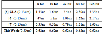
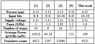
- This section evaluates the performance of our newly proposed pipelined multiplier architecture and compares it with some similar works. Simulation for the multiplier design was done using HSPICE in the TSMC 0.35µm (Level 49) technology. Transistor level simulation results under the supply voltage of 3.3V and 1GHz clock frequency with 0.15ns rise/fall time, are illustrated in Table.2, Table.3 and Table.4.Table.2 shows delays of different methods to remove extra row in Modified Booth algorithm. In higher resolution multipliers our method has a constant and smaller delay (less than 0.62 ns), so it is suitable for high speed pipelined structures, as it causes 4% reduction in power consumption and 5.2% reduction in transistor count.
|
|
|
7. Conclusions
- Due to importance of multipliers in signal processing we designed a high speed low power 16×16-bit pipelined booth multiplier. In this multiplier the last sign bit is removed by using a simple high-speed approach that causes 4% reduction in power consumption and 5.2% reduction in transistor count. Also by using new partial product generation and booth encoder circuits speed of first stages (partial product generation) is increased and with a novel adder multiplication is performed in five cycles. Theoretically number of partial products in a 16×16-bit multiplier is fourth that of an 8×8-bit multiplier. This factor is a good measure for comparison of power consumption and number of transistors between these two multipliers. Table.4 compares some characteristics of this multiplier with other similar works.
 Abstract
 Reference
 Full-Text PDF
 Full-Text HTML