Saeed Roshani 1, Sobhan Roshani 1, Mohammad B. Ghaznavi 2
1Islamic Azad University Kermanshah Branch, Kermanshah, Iran
2School of Engineering, Shahed University, Tehran, Iran
Correspondence to: Saeed Roshani , Islamic Azad University Kermanshah Branch, Kermanshah, Iran.
| Email: |  |
Copyright © 2012 Scientific & Academic Publishing. All Rights Reserved.
Abstract
In this paper, a new low-power profile for mixed-signal design of SARADC is presented. In this profile, frequency dependency of the design power rather than the conventional supply voltage is emphasized. According to this frequency dependency, a new method for low power design in the mixed-signal domain is presented. In this method, whole system is divided into clocked parts and non clocked parts subsystem. Accordingly, a new formula for power consuming in the mixed signal domain is offered. Evaluation results show that when the frequency of a mixed signal system drops down, the ratio of power consumption in analog and digital units have different patterns. In this respect, for our target study of SARADC the power share in analog is about constant while the share of digital sections is rapidly reduced. This means that to reduce the total power, the analog section must be redesigned. The SARADC has a major analog unit as a comparator. In this paper, a new comparator is developed that reduced the analog part share from 89% at 100 KHz to 72% at 100 KHz. The frequency of the target design is selected in range 50 KHz - 200 KHz, which is the conventional range of operations for ADC in Wireless Sensor Network (WSN) nodes. Therefore, proposed new SARADC design is fully suitable for WSN node applications. The proposed SARADC is designed and simulated in 90nm CMOS with the total average power of 4.96µW at 100 KHz.
Keywords:
SARADC, Low Power Design, Mixed Signal Design, Capacitor Array
1. Introduction
Nowadays, more and more applications are built with very stringent requirements on power consumption. The power consumption is becoming one of the most critical factors for electronic systems, such as wireless systems. The need for the development of low power and low voltage circuit techniques and system building blocks has been increased by high importance of the energy consumption[1].In the mixed-signal design, both parts of analog and digital must be modeled and simulated together. The rate of power consumption and proper functionality in analog and digital sections are different. The mutual effects of analog and digital sections are also remarkable. Successive Approximation Analog to Digital Converter (SARADC) is a mixed-signal design. The Wireless Sensor Network (WSN) node is a good sample of mixed signal design. Digital converters are vital and widely used in mixed signal design and implementation. Analog to Digital Converter (ADC) samples the input analog signal and outputs digitalized bit equivalent.Power profile is a global view of the power consumption in sub-units of a target system. This schema is useful with equal validity in both of analog and digital sections. This means that for our target mixed-signal design like WSN node power profile is useful. Power profile enables to have more efficient design. Evaluations show that in the SARADC used in WSN, the comparator is a major unit and consumes most of the total power. Therefore, having low power comparator results in a low power SARADC. In this work, a 6-bit SARADC with 90nm CMOS technology at 1v supply voltage with Hspice is designed and simulated. And reduced the power consumption of ADC with the presented method. The proposed design is best suitable for WSN applications. This paper is organized as follows: Mixed signal domain is briefly described in second section. Comparator as high power consumption part of the SARADC introduced in section three. Power profile and low power comparator design are explained in section four and five. The measured results are described in section six, and finally, the conclusion is expressed in section seven.
2. Mixed-Signal Domain
2.1. Mixed Signal System Division
Due to studies done on the mixed-signal domain it is seen that the main system can be divided into two subsystems which are clock dependent part and clock independent part thus those parts of the system that need clock to act correctly, considered as specific group which shown as clocked system in Figure 1 and other parts of system that work properly without clock, considered as clock independent system. This division can be seen in Figure 1. All digital circuits such as counter, decoder and registers need clock pulses to work correctly thus they belong to the clocked system. Most analog blocks such as comparator acts independently of the clock pulses therefore considered as non clocked system. All digital circuits such as counter, decoder and registers need clock pulses to work correctly thus they belong to the clocked system. Most analog blocks such as comparator acts independently of the clock pulses therefore, considered as non clocked system.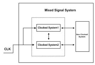 | Figure 1. Mixed signal system division |
2.2. Power issue in mixed signal domain
This division is important to achieve prefect low power design. Obviously the clock rate rises by frequency increasing, Because of dependence of clock pulses on the circuit operating frequency, thus the power consumption of clocked system rises by frequency increasing. We can say that clocked system power consumption has direct relation with frequency rate. On the other hand non clocked system has a frequency independent performance and approximately their power consumption doesn't depend on value of circuit operational frequency. Typical power consumption model can be seen in Figure 2. That in this figure NCS power shows the power consumption of Non-Clocked System and CS power shows the power consumption of Clocked- System and total power consumption is the sum of these two parts.The following equations are expressed for power consumption in mixed-signal circuits. The total power is equal to sum of the power consumption of individual and clock dependence sub systems, that be inferred in Equation (1). | (1) |
Where  is the total power consumption and
  show the power consumption of the clocked and non-clocked system.In Equations (2),(3) frequency dependence and independence terms are considered for each clocked and non-clocked systems.
  | (2) |
 | (3) |
Where 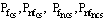 are frequency dependent and independent terms of clocked system and non-clocked system and
  is Kronecker delta which,
  can be 0 or 1. With assuming
 = 1, the first term in Equations (2), (3) shows the value of the power consumption of frequency dependent section at specific frequency point. And second term in these equations represents the value of the power consumption of frequency independent section at the same frequency point.The value of power consumption of clocked and non-clocked system can be shown in Equation (4) at each frequency points and total power consumption is sum of these two terms.
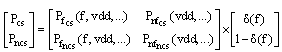 | (4) |
Due to Equation (4) power consumption for various parts of the system can be calculated at each frequency point. This is so important because this is helpful to have prefect design in a special domain with specific conditions. For example, designed SAR-ADC in WSN applications that low power design is the main requirement for these applications and 50 KHz -200 KHZ is conventional frequency range for this domain. To find behavior of the system, we should be more familiar with blocks of ADC. In following sections comparator has been introduced as the major power consumption block of ADC and after that a new formula for power consumption versus frequency will be presented base on these equations.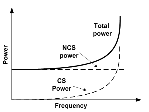 | Figure 2. Typical model for mixed signal power consumpion |
3. SAR ADC Architecture
SAR structure works with single comparator that is suitable for low power design. In this design, the number of bits and resolution is not related to the number of used comparators and in turn gains to have more focus on the low power with emphasis on a single comparator.
3.1. Comparator
In the WSN applications with sampling rates of (50Ks/s-200Ks/s) the rule of comparator is more critical. In a WSN node more than 70% of the total power of SARADC is used in comparator. This means that in the low power targeting for SARADC, comparator is the suitable block for emphasis. The schematic of an ultra low power comparator is illustrated in Figure 3, this structure is used in[4, 5]. The shown structure is very low power. In this comparator, there is a one pair of NMOS at the input. This pair is not working properly in the low voltages (near zero). Therefore, the comparator is not working properly in the subthreshold region of[0-Vth]. The comparator of Figure 3 works very fine for the voltage range of[Vth-Vdd]. In this region the comparator works with a very low power. The PMOS input pair for the comparator in turn is not working properly in the near VDD rang of[Vdd-vth, Vdd].
3.2. Optimized Comparator
The idea of combining NMOS and PMOS pair at inputs is first introduced in[7]. Based on the proposed idea in[7], the combined input pair of PMOS and NMOS is applied for input of Figure 3 and proposed comparator is resulted that shown in Figure 4. Optimize comparator not only overcomes the rail-to-rail swing problem but also results in a very low power design. The approach to change proposed comparator as a low power comparator is discussed in section five.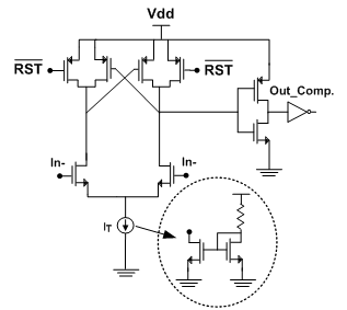 | Figure 3. Ultra low power comparator circuit schematic[3] |
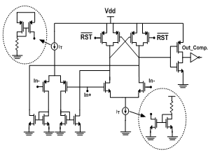 | Figure 4. Optimized comparator circuit schematic |
4. Power and Power Profile
ADC converter contains some building blocks. Each block has its own share in the total power consumption.For example, the power of sub-blocks in SARADC for two frequencies of 10MHz and 100 KHz are presented in table 1 and depicted in Figure 5.| Table 1. Average Power of SARADC Sub-Blocks at Two Different Frequencies |
| | Parts | Average powerAt 100KHz | Average powerAt 10MHz | | Comparator | 10.334 µw | 10.959µw | | Registers | 218.965nw | 10.91 µw | | Counter | 81.735nw | 5.368 µw | | Decoder | 67.002nw | 3.828 µw | | Others (switches, capacitor Array) | 1.03 µw | 2.996 µw | | Entire ADC | 11.732 µw | 34.031 µw |
|
|
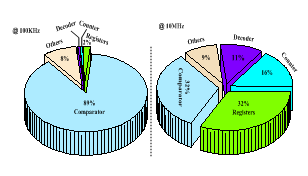 | Figure 5. Power profile of sub-blocks in SARADC for two frequencies of 100 MHz and 100 KHz |
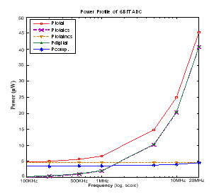
It is seen that at f=10MHz, digital parts including register, counter and decoder have a valuable impact on total power. As frequency drops down, the share of digital sub-sections is reduced. This is due to the main dependency of power to frequency in digital systems. Investigations show that there is a relation between sub-blocks power and operating frequency that is shown in Equations (1) to (4).According to the cases discussed above, the ADC is divided into clocked and non-clocked sections and power consumption for these parts shown in Fig. 6. As is seen in this figure the sum of power consumption of clocked and non-clocked system is equal to total power consumption. Also spliced power of analog and digital sub-sections is illustrated in log. scale in Figure 6.Digital parts consist of three sections registers, counter and decoder and analog parts consist of comparator. As can be seen the power consumption curve of clocked system is similar to digital part power consumption curve and power consumption curve of non-clocked system and analog section are identical. The total power consumption curve consists of two asymptote curves, in high frequencies the power consumption of the digital curve is asymptote and in low frequencies the analog power consumption curve is asymptote for total power consumption curve.As seen the Fig. 6 confirm proposed model for mixed-signal that illustared in the Fig. 2.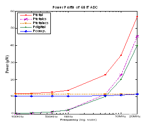 | Figure 6. Power profile for SARADC with spliced share of Analog and Digital sub-sections in log sclae |
Due to Fig. 6, Equation (5) is presented for power consumption of ADC. In this equation, the first column arrays of the matrix show the frequency dependent term of power and second column arrays show the frequency independent term of power.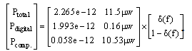 | (5) |
The importance of these equations and curves is that show the main blocks of power consumption at specific frequency range. In WSN applications can be found the power consumption of digital part is negligible but comparator is the major power consuming units that consume 89% of total power in this range. This shows us we should optimize the comparator to achieve low power ADC. Therefore, the power consumption of the comparator is lowered. This process has been explained in following section.
5. Low Power Comparator Design
The presented formula is helpful to optimize the ADC. According to this formula, it is seen that comparator is major power consumption part of ADC. This part consumes power independent from frequency changes. Therefore, to have low power ADC comparator should be improved. In the comparator, the bias and bias currents are implemented by typical CMOS current mirrors. In the current mirror like shown in Fig. 4, the current ratio in the mirror side is proportional to the aspect ratio of MOS transistors or  . To have ID2 much larger than ID1, it is sufficient to select
  much larger than
 . This modification results in reasonable results in the gain of a low power design.As seen in the Fig. 4 the comparator current is based on two current mirror circuits. To have low power design, from one side, the value of R must be selected as large as possible to control and reduced the current derived from the supply. On the other hand, the ration of W/L must be increased to have smaller currents.From the practical view point, the larger resistance occupies more area in the chip layout and is not interested. To solve this problem, the resistors are replaced with MOS transistors. In this case, the gate of the transistors is connected to either Vdd or Gnd. This also removes the need to additional bias voltages. The spliced power share in proposed SARADC working at 100 KHz is summarized in table 2. It is seen that the total power is reduced to below 5µW.
| Table 2. Average power of proposed SARADC sub-blocks at 100 KHz |
| | Parts | Average power At 100KHz | | Comparator | 3.557µW | | Registers | 220.894nw | | Counter | 81.718nw | | Decoder | 67.123nw | | Others (switches, capacitor Array,..) | 1.03µW | | Entire ADC | 4.961µW |
|
|
The power profile of proposed SARADC with reduced share of comparator is depicted in Figure 7.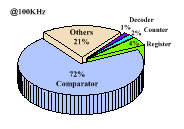 | Figure 7. The power profile of our proposed SARADC |
 | Figure 8. Power profile for optimized SARADC with spliced share of Analog and Digital sub-sections in log. scale |
The new low power ADC confirms the presented general formula where the constant term of power consumption is reduced. Equation (6) shows a new special formula for optimized ADC. The power profile versus frequency of the proposed SARADC for the frequency range of[100 KHz-20MHz] in log. scale is illustrated in Fig. 8 that confirms the results. 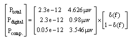 | (6) |
6. Measured Results
6.1. Measured Results
In Fig. 9 a typical 1024 points FFT of the output spectrum in the input frequency of 1.5625 KHz with 1v supply is depicted. The ENOB of the proposed SARADC is ENOB=5.87.
6.2. FOM Calculation
FOM is calculated with Equation (7).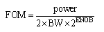 | (7) |
Hence for Average Power=4.97µW and ENOB=5.87 with input frequency of 1.5625 KHz, FOM is 849fj per Conversion step.The overall performance of the proposed SARADC is shown in Table 3. And In Table 4, summary of comparison of proposed SARADC versus five other related designs is presented.| Table 3. Overall Specs of the Proposed Low-Power SARADC |
| | Specs | Measured | | Technology | 90nm CMOS | | Voltage Supply | 1V | | Input Range | Rail- to – Rail | | Sampling Rate | 100KHz | | ENOB(at:1.5625KHz) | 5.876bit | | Power Dissipation | 4.97 µw | | FOM | 0.849 /step |
|
|
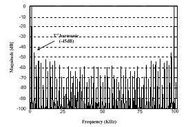 | Figure 9. Typical FFT for input freq. of 1.5625 KHz and 1v supply voltage |
7. Conclusions
A 6 bit SARADC with 100Ks/s at VDD=1V is designed for WSN applications. A power profile for frequency of mixed signal design is studied and the impacts of analog and digital sub sections are studied. Our study shows that the impact of analog section in the lower range of frequencies is more than digital section. We focused on analog section and designed a low power comparator. According to this idea, new model for power consuming is presented in the mixed signal system. Simulation results confirm the presented model. The total power of the proposed SARADC that is optimized with the new method is about 4.97µW at 100 KHz.| Table 4. Comparison of the Proposed SARADC With Another SARADCs |
| | sources | [5]a | [5]b | [6] | [7] | [8] | [1] | This work | | Technology (CMOS) | 0.18µm | 0.18µm | 0.25µm | 0.18µm | 0.25µm | 90nm | 90nm | | Resolution | 8bit | 8 bit | 8 bit | 12 bit | 6 bit | 8 bit | 6 bit | | SupplyVoltage | 1v | 0.9v | 1v | 1v | 2.5v | 1.2v | 1v | | Sampling Rate(S/s) | 400k | 200k | 100k | 100k | 1M | 1.4k | 100k | | ENOB (bit) | 7.31 | 7.58 | 7.9 | 10.55 | 5.53 | 7.8 | 5.9 | | Power Dissipation | 6.15µw | 2.47µw | 3.1µw | 25µw | 1.19mw | 13.4 µw | 4.97µw | | FOM (fj/step) | 97 | 65 | - | 167 | 1288 | - | 849 |
|
|
ACKNOWLEDGEMENTS
The authors would like to thank Dr. M. Jalali for his helps and support.
References
| [1] | G. Beanato, "Design of a Very Low Power SAR Analog to Digital Converter," Master of Science, Department of Electrical Engineering, The EPFL University, 2009. |
| [2] | J. Kahn, et al., "Next century challenges: mobile networking for “Smart Dust”," 1999, pp. 271-278. |
| [3] | M. Last and S. Kristofer, "Smart dust: Communicating with a cubic-millimeter computer," IEEE Computer, vol. 34, pp. 44–51, 2001. |
| [4] | S. Ahmad, "Design of a high-Speed CMOS Comparator," Master of Science, Department of Electrical Engineering, Linkoping University, 2007. |
| [5] | H.C. Hong, G.M. Lee, “A 65-fJ/Conversion-Step 0.9-V 200-kS/s Rail-to-Rail 8-bit Successive Approximation ADC” IEEE J. Solid-State Circuits, vol. 42, no. 10, Oct. 2007. |
| [6] | M. Scott, et al., "An ultra-low power ADC for distributed sensor networks," ESSCIRC proceedings, September, pp. 24-26, 2002. |
| [7] | N. Verma and A. Chandrakasan, "An ultra low energy 12-bit rate-resolution scalable SAR ADC for wireless sensor nodes," IEEE Journal of Solid State Circuits, vol. 42, pp. 1196-1205, 2007. |
| [8] | P. R. Johnson, M. C. Wasio, and J. D. Wigton, "A Low Power Reconfigurable SAR ADC", University Of Michigan, design contest, winter 2006. |
 Abstract
 Reference
 Full-Text PDF
 Full-Text HTML