Rahim Fathi , Mehdi Esmaeil Pour , Sadegh Mohamad Zadeh
Department of Electrical Engineering, Urmia branch, Islamic Azad University, Urmia, Iran
Correspondence to: Rahim Fathi , Department of Electrical Engineering, Urmia branch, Islamic Azad University, Urmia, Iran.
| Email: |  |
Copyright © 2012 Scientific & Academic Publishing. All Rights Reserved.
Abstract
In this paper the circuit to produce the current mode membership function including OTA and MIN, MAX circuits has been presented. The ability to produce very linear triangular, trapezoidal, s-shape and z-shape functions for applications of neuron-fuzzy programming with controlling voltages is applied. The circuit is designed with simple structure, high dynamic range, low power consumption and area is the speed and accuracy is high. At the end the simulation results with the software HSPICE (49 levels) of 0.35μm CMOS standard processes is presented. Layout of circuits on the surface is about 5μm×36 μm.
Keywords:
Fuzzifier, Fuzzy controllers (FLC), Neuro-Fuzzy, OTA Structure, Membership Function Circuit
1. Introduction
The design of fuzzy systems by Professor Lotfi Zadeh, that uncertainty of physical phenomena introduced, it was started. Fuzzy controllers (FLC) in a variety of control systems for easy and does not need accurate mathematical models are used. Fuzzy systems may be either a software or hardware used. The software can be effective when the speed and capacity is not needed, which is generally on the implementation of software systems of Neuro-Fuzzy has focused. The software is not suitable for high speed applications, so for solution of problem the hardware method (designed IC) for design is used. The analog circuits because used of parallel Structures are with high speed that the speed limit in this circuit is only due to the delay signal transmission system and also due to the low number of transistors and low-volume system to digital system used analog system. In the paper produced four types of membership functions using OTA structure has been studied.CMOS circuitry for systems of FLC has been presented in recent papers; each has with advantages and disadvantages. fuzzifier circuits presented in reference[3] and[5] are unable to produce the sigmoid functions and their simultaneous production cause increase power consumption and increase the area.In reference[3] as well as the increase current resources and number of transistors to increase the outputs, Power consumption and Area is more. fuzzifier circuit presented, is an OTA-based circuits with MIN, MAX circuits that is flexible programming capability, high accuracy and dynamic range, low power consumption and simple structureOTA structure is described in Section 2; in section 3, circuit to produce slope and How to change their slope; in Section 4; the MIN, MIN circuits, layout and circuit simulation in Section 5 and conclusions are presented in Section 6.
2. The Ota Structure
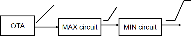
In general, fuzzy systems are composed of three main parts:A. membership function circuit (Fuzzifier)B. apply the fuzzy rules, singletone and consequent circuitsC. defuzzifireDifferent functions in the fuzzy used that in this paper to produce four of them (triangle, trapezoid, s-shape, z-shape) is mentioned. To Production functions for the blocks listed in Figure 1, we perform:And for the production of membership functions, s-shape and z-shape as the block (2) we pass the output of an OTA circuit of MAX and then MIN circuit.
3. Membership Function Circuit
A. slope circuit:Circuit (Fig. 3) to produce a linear slope function is designed: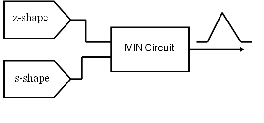 | Figure 1. General block structure of the OTA |
 | Figure 2. Block of s-shape and z-shape |
 | Figure 3. slope circuit |
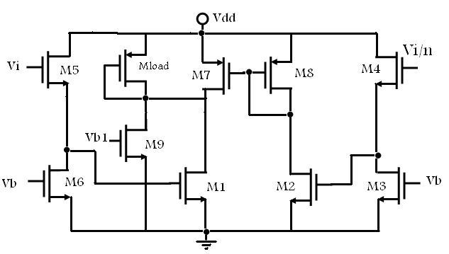
Transistors M3, M4, M5 and M6 as a buffer for Shift Register function on the horizontal axis to be used, so that the M3, M6, with gate–source voltage Vb, creating a current that must from the M4, M5 passes.Thus the difference gate- source voltages of the M4, M5 are Vb and the gate voltages of the M4, M5 to Vb drops.If the process is only include Nwell for linearity more buffers (the body) can be used to Pwell.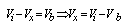 | (1) |
At circuit in Figure 1 size of the transistor, M2 is equal n2 to the transistor M1 (n is ratio the input voltage) and the size of other transistors symmetrical by M1 transistor is placed. AndThe size of transistors Mload, M7, M8 also coincides. (Providing the bulk of the NMOS transistors are segregate, PMOS can be used)In the circuit voltage applied to gate M1 creates a current that are the non-linear relationship (with a good approximation is a quadratic equation) with gate- source voltage and the generated Current by the M2 transistor is so designed that by the non-linear part of the transistor M1 is equal. Thus the current by mirror current M7 and M8 subtracted of the current M1 and current linear part of transistor M1 is entered Mload.In this case, the currents respect will be as follows: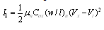 | (2) |
 | (3) |
 | (4) |
That the current I2 drawn from M8 and is mirror the M7. | (5) |
Id is current of M9 transistor. | (6) |
By situation  will be
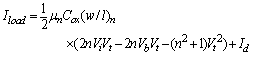 | (7) |
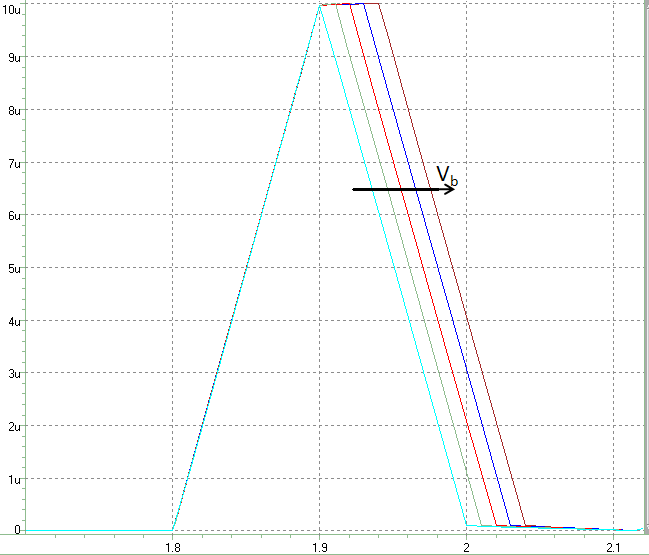
That in the relationship the current Iload varies linearly by Vi. By Vb for the shift on the horizontal axis and by id for the shift on the vertical axis is used.Output OTA circuit is proposed as follows:To determine the slope of membership function is made, two methods are provided:When designing the slope of membership function can be determined by the size of transistors.Changing the slope by control voltages that can be achieved by changing the threshold voltage by applying a voltage to the transistor bulk M1 and M2 is done.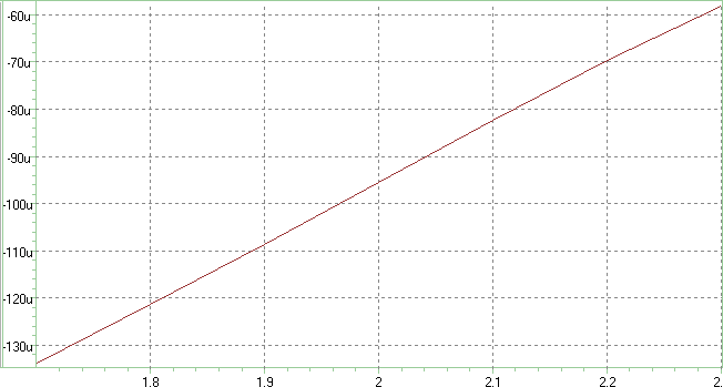 | Figure 4. The sample of slope function produced by the OTA circuit |
As the simulation in Figure 5 shows the variation of current slope with increasing bulk’s voltage, linearly decreased.But Since the high changes of bulk’s voltage, current output be non-linear. Therefore amplitude of these changes should not be excessive. Relation of Bulk-source voltage and threshold voltage is as follows: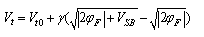 | (8) |
 | Figure 5. change of Slope of the production functions using the bulk voltage |
In relation (8) Vt0 threshold voltage is the voltage per VSB =0 is called zero threshold’s voltage and Parameter gamma (γ) is coefficient of the body (the body).To obtain a negative slope, we decrease the output of circuit (3) from a constant dc current. In figure (5) Change the slope of the membership function per bulks voltage of zero and 0.4 is drawn:For high linearity of circuit can the slope of the functions by the size of transistors in the design phase was determined.
4. MAX and Min Block
4.1. MAX Circuit
This circuit is to that it can be extended to more inputs. mechanism of the above circuit so that when the current Iin1 is larger Iin2 the voltage of node A and Consequently the node B and C will increase and because the current Iin1 assumed is less than Iin2 so Voltage nodes E and D, respectively, are lower than the voltage of node A and B. thus M3 due to less the voltage between drain and source of his enters into the linear region and M7 due to less the voltage between gate and source is cut off and maximum current through M5 to transmit output. (Of course providing the Differential input current is low; Transistor M3 can be at active area and the circuit works just as MAX circuit and the Differential current by reducing the voltage between the drain -source M3 is compensated)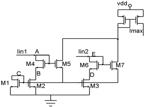 | Figure 6. MAX circuit (All transistors have the same size) |
 | Figure 7. MIN circuit (inputs are Complemented and together compared ) |
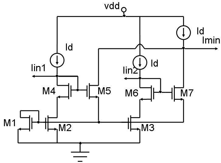
4.2. MIN Circuit
MIN circuit presented providing in Figure (8). The mechanism of the above circuit so that first Iin1 and Iin2 currents through the Id were complemented and their complement with MAX circuit is compared. That their maximum complementary of inputs will equal to the minimum input and Min current to transmit output.
5. Simulation Results and Circuit Layout
Simulation results using the Hspice software provided in the standard 0.35μm CMOS. Total circuit power consumption is 200mw and dimensions of the layout are approximately 15μm ×36μm.Membership functions are generated as follows: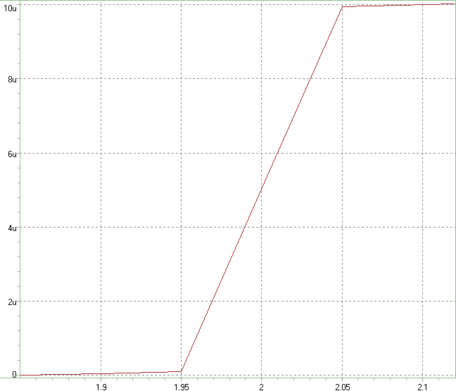 | Figure 8. S-shape membership function |
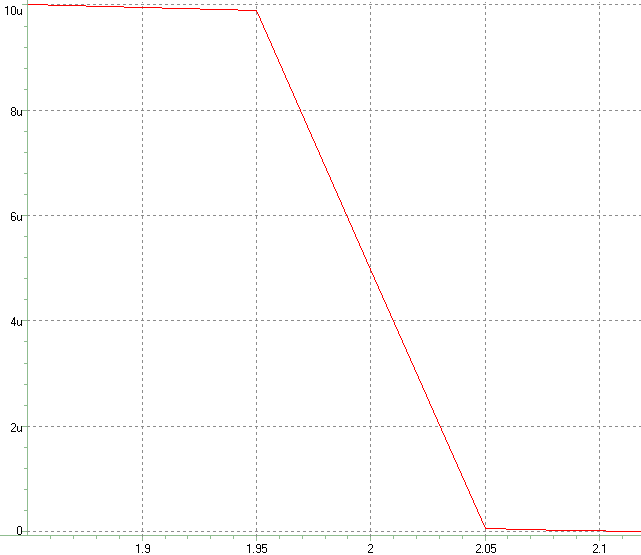 | Figure 9. Z-shape membership function |
 | Figure 10. Change of width of the membership function |
In Figures 11 and 12 the ability to change the width and slope of membership function is shown: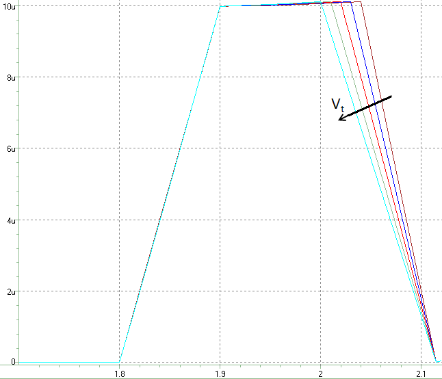 | Figure 11. Change of Slope of the membership function |
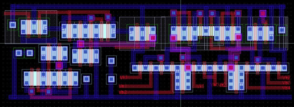 | Figure 12. Circuit Layout |
6. Conclusions
In the paper a circuit to produces a membership function programmable in CMOS technology is presented that can the four membership functions, triangular, trapezoid, z-shape, and s-shape Linearity with very high accuracy is produced.Circuit designed moreover the capabilities is ability to increase the number of inputs and outputs with increase the small number of transistors that This reduces overall power consumption and chip area is.
References
| [1] | L. A. Zadeh, “Fuzzy Logic,” IEEE Computer Magazine, pp. 88-93, April 1988. |
| [2] | Hamed Peyravi , Abdollah Khoei , Khayrollah Hadidi, “Design of an analog CMOS fuzzy logic controller chip,” Elsevier Science J. Fuzzy Sets and System 132(2002), PP.245-260. |
| [3] | Wei-zhi Wang , Dong-ming Jin,“ Neuro-fuzzy system withhigh-speed low-power analog blocks,” Elsevier Science J.Fuzzy Sets and System 157 (2006), PP. 2974-2982. |
| [4] | Yasuhiro Ota and Bogdan M. Wilamowski, "Current-Mode CMOS Implementation of a Fuzzy Min-Max Network" |
| [5] | Wei-zhi Wang , Dong-ming Jin,“ CMOS design of analogNeuro-fuzzy system with Improved circuits,” Proc. IEEE 7thInternational Conference on Solid-State and IntegratedCircuits Technology, Vol. 2, PP. 1591-1594, Oct. 2004. |
| [6] | Y. Ota and B. M. Wilamowski, “VLSI Implementation of a ProgrammableCurrent-Mode Neural Network,” Proceedings: Intelligent Engineering Systems Through Artificial Neural Networks, ANNIE’94 Conf., St. Louis, USA,Nov. 1994, vol. 4, pp. 71-76. |
| [7] | R.G. Carvajal, A. Ramirez Angulo, J. Martinez Heredia,“High-speed high-precision min/max circuits in CMOStechnology,” IEE Eletron. Lett. Vol. 36, NO. 8, PP. 697-699,April 2000. |
| [8] | J. R. Angulo and R. P. Loera, “Low Voltage Current-Mode and Voltage-Mode Min and Max Circuit Building Blocks for Analog CMOS Fuzzy Processors,” Proceedings: 3rd Int. Conf. on Fuzzy Logic, Neural Networks and Soft Computing, Iizuka, Japan, 1994. |
| [9] | J. Ramirez-Angulo, G. Ducoudary-Acevedo, R. G.Carvajal, A.lopez-martin,“ Low-Voltage High-Performance Voltage-Mode and Current-mode WTA Circuits Based on FilippedVoltage Followers,” IEEE Trans. On Circuits and Systems-II, EXP Briefs, Vol. 52, NO.7, PP. 420-423, JULY 2005. |
| [10] | J. Ramirez-Angulo, J. E. Molinar-Solis, S.Gupta, R. G.Carvajal, A. lopez-martin,“ A High-Swing,High-SpeedCMOS WTA Using Differential Flipped Voltage Followers,”IEEE Trans. On Circuits and Systems-II, EXP Briefs,Vol.54, NO.8, PP. 668-672, AUGUST 2007. |
| [11] | S. Kazemi Nia, A. Khoei, Kh. Hadidi,“ High Speed HighPrecision Voltage-Mode MAX and MIN Circuits,” 13thIEEE International Conference on Electronics, Circuits andSystems, 2006. ICECS apos;06. Volume , Issue , 10-13, PP.272 – 275, Dec. 2006. |
 Abstract
 Reference
 Full-Text PDF
 Full-Text HTML