V. M. Deshmukh1, A. J. Patil2, P. V. Thakre1
1Dept. of E&TC, SSBT’S C.O.E.T. Jalgaon, India
2Principal, SGDCOE Jalgaon, India
Correspondence to: V. M. Deshmukh, Dept. of E&TC, SSBT’S C.O.E.T. Jalgaon, India.
| Email: |  |
Copyright © 2015 Scientific & Academic Publishing. All Rights Reserved.
Abstract
This paper presents the development of a 30KVA three phase sinusoidal PWM inverter using DSP. Generation of DSP based PWM signal to control the voltage source inverter substantially help the development of modern inverter which is required to work on different KVA ratings or different loads for various applications. Since experimentation of different KVA ratings inverter models on hardware being relatively expensive, the use of MATLAB/Simulink helps to check the performance of these models and validate through the comparison analysis with the conventional techniques. It is possible because the algorithm required to generate the PWM signals is written in C language so it can be reused easily and this flexibility provides in terms of changing the switching frequency for the desired inverter output voltage. In this paper the algorithm development methodology and the experimental results along with simulation model are presented which show the effectiveness of the proposed algorithm.
Keywords:
PWM inverter, DSP controller, CCS, MATLAB interface, Digital model
Cite this paper: V. M. Deshmukh, A. J. Patil, P. V. Thakre, Development of Matlab/Simulink Model for Three Phase PWM Inverter and Hardware Implementation and Testing Using DSP with Nonlinear Load, International Journal of Control Science and Engineering, Vol. 5 No. 1, 2015, pp. 1-9. doi: 10.5923/j.control.20150501.01.
1. Introduction
A practical inverter consists of battery bank or PV connected battery for energy storage and a static inverter-filter system to convert a dc voltage to a sinusoidal ac output. Now a day’s photovoltaic (PV) power systems offer a sustainable alternative to fossil-fueled power plants, providing lower long-term operating costs. The utilization of natural DC voltage from the PV system at different condition, a smart inverter is required. The recent developments in power semiconductor devices and fast digital signal processing hardware the inverters are becoming a major and common devices which plays a vital role in various application such as data processing systems, home appliances, patient health care centers and critical telecommunication link. The introduction of high power voltage source inverter is relatively eased due to favorable properties of IGBT such that high power handling capability. Despite this advantage of IGBT the switching losses are the major issue and it causes the low current distortion and harmonic losses. One of the interesting solutions that minimize the above problem is use of high performance pulse width modulation [1]. The inverter is operated with a pulse-width modulation (PWM) strategy under the closed loop control to realize the desired output waveform with reduced harmonics. Harmonic contents are the major parameter responsible for the diluting the sinusoidal ac output so the control of the inverter switching is important to minimize the harmonic content of the output voltage. The difficulty in successful switching control operation stems from the output impedance of the inverter filter. Low output filter impedance can be realized via a high inverter switching frequency. Modulation is a process where some character (width in this case) of carrier signal is changed in accordance with the intensity of modulating signal. PWM uses an analog signal to modulate the width of pulses whose durations are proportional to the amplitude of the modulating signal at that instant. Control of the PWM inverter is realized with high-speed feedback loops, where the actual output waveform is compared with a sinusoidal reference [2]. The error is used to modify the inverter switching of bipolar transistors to create a PWM representation of an ac sine wave. The analog controls present a number of potential drawbacks for both manufacturers and users. Analog controls rely on a large number of discrete components and connection which creates relatively high hardware cost. As a result, the up gradation of inverter is impossible without hardware changes and each new model requires a redesigned, remanufactured control system. Solution of this issue finds in the low cost microcontrollers or digital signal processors (DSP). Although the inverters has traditionally been designed as analog circuitry, digital inverters are now preferred. DSP offer sophisticated control algorithms with highly flexible software, the ability to add user interfaces, reduce components, introduce testing procedures, and increase reliability. The DSP controlled inverter system employs software controlled harmonic conditioners with the ability to dynamically adapt to changing load conditions for automatic compensation of the load harmonics without manual intervention. Thus the application of advanced signal processing using a DSP operates to provide sinusoidal load voltages even under varying nonlinear load conditions, while eliminating the need for large passive filters. This paper presents the hardware model of DSP control of three phase 30 KVA inverter systems supplying nonlinear loads to continuously provide sinusoidal load voltages and DSP-based algorithm to generate sine wave PWM signals is introduced. Experimental implementation based on a TMS320F2812 DSP is presented along with algorithm development process and flowchart. It also presents the simulation model of PID controller three phase 5KVA inverter with PV source supplying nonlinear load. Finally system experimental results and simulation results are demonstrated.
2. Digital Signal Processor
A Digital Signal Processor is a specific device that is designed around the typical mathematical operations to manipulate digital data that are measured by signal sensors. The objective is to process the data as quickly as possible to be able to generate an output stream of ‘new’ data in “real time”. One important feature regarding the power converters is the real-time processing that is the output signal is produced at the same time when the input signal is being acquired.DSP is the natural choice as it able to perform high speed calculations required in power electronics. The innovation of DSP control into power electronic designs is an excellent example of the advantages provided by major technological advances. By replacing classic control with DSP control, the primary advantages are achieved by replacing hardware with flexible software. The advantages are even more dramatic because they don’t just extend to reducing cost and increasing performance over classic designs [3-4]. DSPs are used in multiple applications in power electronics including AC motor drives, high-frequency converter control, motion control, robotics and real-time testing and monitoring. Because of the DSP’s special architecture, it is more useful than a general-purpose microprocessor for the high-speed processing applications and real-time systems such as control system. DSPs are built with Harvard architecture, and this configuration employs separate program and data buses. The benefit of this arrangement is the increased speed because instructions and data can move in parallel instead of sequentially. DSPs, like many advanced microprocessors, use pipelining to operate on several instructions simultaneously. Many DSP chips include input/output (I/O) functionality, timing circuitry, direct memory access (DMA) controllers and high-speed memories on-chip.DSP instruction sets efficiently handle mathematical operations common to many algorithms that are repeatedly executed in time-critical loops. For example, digital filters, which are often used in signal processing and control applications, are implemented using recursive difference equations of the form: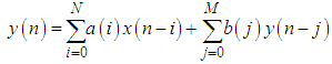 | (1) |
The equation states that any output can be computed as a weighted sum of the input at the present time, past inputs and past outputs. Each step in this computation involves a multiplication and addition. The multiply and accumulate (MAC) instruction in DSPs performs this in a single instruction cycle. In contrast, in a typical fixed-point microprocessor, a “multiply” and “add” typically executes in 15 to 20 machine cycles. MAC is the one instruction that most distinguishes DSPs from other micros. DSPs also significantly increase execution speed by performing multiple operations in parallel. For instance, in the same instruction cycle that a MAC operation is being performed, a parallel data move can be carried out. Thus, the special DSP instructions supplement the computational speed of DSPs and make them ideal for high-performance real-time applications.
3. Architecture of TMS320F2812
Texas instruments has developed the DSP solutions that are driving digital control by providing the industry's high performing and code efficient DSPs [5]. The TMS320C2000 family of DSP controllers set the standard for performance and peripheral integration by offering a unique combination of on-chip peripherals such as flash memory, ultra-fast A/D converters, PWM modules and robust CAN modules. This architecture optimized for C/C++ and it offer good code efficiency, and uniquely enables customers to develop their code in virtual floating point via the IQ math capability. The TMS320C2812 supports multiple bus architecture, whose memory bus architecture contains a program read bus, and data read bus and data write bus. The 32-bit-wide data busses enable single cycle 32-bit operations. The F281x and C281x implement the standard IEEE 1149.1 JTAG interface. Additionally, the TMS320C2812 supports the real-time JTAG mode of operation including the contents of memory, peripheral and register locations; that is to say, the real time analysis is allowed. To perform register to register operation it is required to execute most of the instruction and the F2812-CPU is capable to do this function. It has 32 x 32-bit MAC along with its 64-bit processing capabilities. For the project development in DSP the JTAG-interface device plays a vital role to support real-time data exchange between the DSC and a host during the debug phase. It is possible to watch variables while the code is running in real time, without any delay to the control code. Memory bus consist of 22 address lines and 32 data lines the priority of Memory Bus accesses are Highest: Data Writes, Program Writes Data Reads & Program Reads and Lowest: Fetches.
4. Event Manager
Event Manager (EV) is the most powerful modules and core of this manager is similar to DSPs core timer units called “Timer 0, 1 and 2” [6-7]. DSPs core timer have a 32-bit count-down register, which generates an interrupt when the counter reaches zero and thereafter it is automatically reloaded with a 32-bit period value. Whereas Event Manager Timer units called "Timer 1, 2, 3 and 4", is a 16-bit counter/timer unit. The eZdspF2812 DSP board is used for generation of PWM control signal and PWM algorithm requires a time reference. This time reference is generates by using General Purpose (GP) Timer of EV Modules. This signal is a digital pulse with binary amplitude and using the EV-logic, the frequency and/or the pulse width of these output signals can be modify. When an internal control scheme is applied to modify the shape of the signals during run time, this is calling ‘Pulse Width Modulation’ (PWM). The C28x is equipped with two Event Managers, called EVA and EVB. These are two identical hardware units; two 16-bit timers within each of these EVs generate the time base for all internal operations. In case of EVA the timers are called ‘General Purpose Timer’ T1 and T2, and in case of EVB they are called T3 and T4. The EV modules include: General-purpose (GP) timers and Full compare/ PWM units. There are two GP timers in each EV module. Each GP timer has A 16-bit timer: up-/down-counter, TxCNT, compare register, TxCMPR, period register, TxPR and control register, TxCON all for reads or writes. There are three full-compare units on each event manager. These compare units use GP timer1 as the time base and generate six outputs for compare and PWM-waveform generation using programmable dead-band circuit. The state of each of the six outputs is configured independently. In many power electronics applications like inverter there are two switches on each legs and the turn-on periods of the two switches must not overlap with each other in order to avoid a shoot-through fault. Thus, a pair of non-overlapping PWM outputs is often required to properly turn on and off the two switches. A dead time (dead-band) is often inserted between the turning-off of one transistor and the turning- on of the other transistor. This delay allows complete turning-off of one transistor before the turning - on of the other transistor. The dead-band-generator circuit produces two outputs for each compare unit output signal. The output states of the dead-band generator are configurable and changeable as needed by way of the double-buffered ACTRx register. There are deaband registers: DBTCONA, DBTCONB. The capture unit provides a logging function for different events or transitions. ‘Quadrature Encoder Pulse’ (QEP) is a unit that is used to derive the speed and direction information of a rotating shaft directly from hardware signals from incremental encoders or resolvers.A. PWM Waveform Generation using EV Simultaneously eight PWMs outputs can be generated from each event manager. Out of these, six PWMs outputs or three independent pairs by the three full compare units with programmable dead-band and two independent PWMs by the GP timer compares. The procedure to generate a PWM signal with event manager consist of counting modes, GP Timer compare operation and carrier signal generation. Three compare units are in EVA module another three compare units are in EVB module. For generation of carrier signal two counting modes are used, continuous up modes gives asymmetric carrier waveform and continuous up down modes gives symmetric carrier waveform. These modes are controlled by the content of TxCON register.The Figure 1 Shows the symmetric PWM generation with compare units. By using counting modes in each time period (timer values are incremented by one for each clock pulse) the carrier signal is compared with the value stored in the compare register TxCMPR, the + sign in figure 1 indicate the compare matches. PWMx+1 is logic zero and PWMx is logic one before the first match, and the value of the compare register is greater than the value of the carrier signal. PWMx+1 is logic one, PWMx is logic zero between the first and second compare matches, the value stored in the compare register is smaller than the value of carrier signal, as a result of this, the PWM outputs change their states. 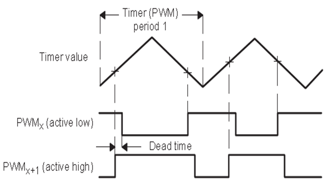 | Figure 1. Symmetric PWM generation with compare units |
B. PWM carrier signalIn this application Event Manager Module (EVB) and General Purpose Timers 3 and 4 (GP timers 3 and 4) of the DSP were used to generate asymmetrical PWM waves. GP timer 3 is configured as follows:* The timer period register T3PR is set to 2500 (desired 10 kHz PWM frequency).* The timer control register T3CON is set to 0x1042 (counting mode, clock source).A continuous up-counting mode is generally used to generate asynchronous PWM. The timer period value is calculated as follows: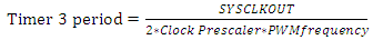 | (2) |
Where: SYSCLKOUT is the CPU clock frequency (150 MHz for the TMS320F2812 DSP) For a new PWM frequency, the period value for GP timer 3 is recalculated and the new value is written to the period register during the program run. It is also possible to modify the switching frequency by means of a digital input. GP timer 4 is used to modify periodically the compare register in order to obtain the desired frequency of the inverter output. In this application the compare registers were updated each timer interrupt to obtain the 50 Hz inverter output voltage. The interrupt is generated upon period match. The period value for this timer is calculated as follows:
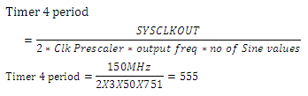 Timer 4 period register value represents the step required to load the next value from the sine table. Modifying this period register value results in changing the inverter output frequency without the need to change the frequency of the modulating signal as in the conventional sine PWM generation.The flowchart in figure 2 shows the DSP signals generation. For the generation of PWM signals considering the three phase inverter following equation are being used.
 | (3) |
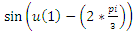 | (4) |
 | (5) |
Based on these equations the source code has been generated for the code composer studio (explained in the next section) to generated the pulse signals for each phase.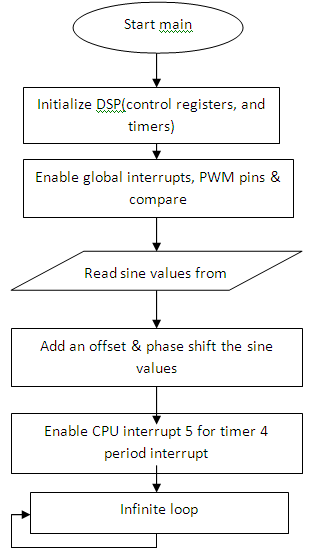 | Figure 2. DSP signal generation flowchart |
5. Working and Analysis of Three Phase Inverter
Basic concept for generation of PWM with close loop control: The dynamics of the system is simplified to a LC low-pass filter connected to the load. Figure 3 is the equivalent circuit of the photovoltaic inverter, where u is the system input (control variable), and Z denotes the output impedance of an unknown load [8-11]. The Equivalent Series Resistance (ESR) of the filter inductor is denoted as rL, and the ESR of the filter capacitor is denoted as rc.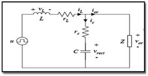 | Figure 3. Equivalent circuit of the photovoltaic inverter system |
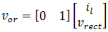
By ignoring the polarity-reversing bridge, the rectified sinusoidal output voltage, vor is obtained. Choosing the filter inductor current iL and filter capacitor voltage vrect as the state variables, the state-space representation and output equation of the system is given by 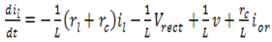 | (6) |
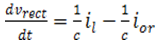 | (7) |
Also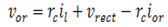 | (8) |
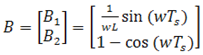
Equation (6) & (7) are represented in matrix form as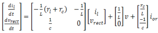 | (9) |
Also equation (8) is expressed as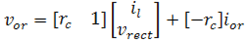 | (10) |
The values of rl & rc are assumed to be very small & are neglected. Thus equation (9) & (10) becomes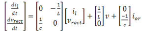 | (11) |
 | (12) |
Based on the equations a dynamic model of the system is represented by block diagram as shown in figure 4.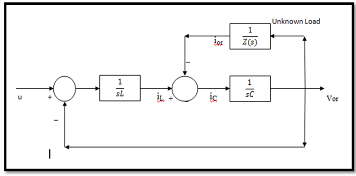 | Figure 4. Dynamic model of the inverter |
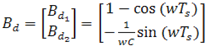
Since the controller is to be implemented using a digital processor, the continuous time space equations are converted into discrete form. The discrete time state space equations with sampling period of Ts are represented as | (13) |
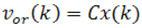 | (14) |
Where 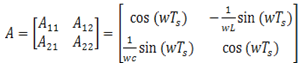

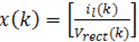 is the state vector &
  is the cut off frequency of the low pass filter in radians/second.For design and development of digital closed loop controller, output voltage and current are sensed and fed to ADC which improves the switching sequence of power switches. The control strategy is classified in two types:-1) Current loop control2) Voltage loop controlIn current loop control, based on the control signal u(k) applied to the PWM modulator, the condition of current loop control is given by:-
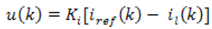 | (15) |
Where iref(k) is reference current based on panel input il(k) is load current. Considering the block diagram for current loop control as shown in fig. 5, the discrete time transfer function G(z) is given by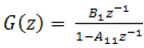 | (16) |
Based on the discrete time model developed for the inverter system.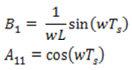 Thus
Thus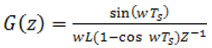 | (17) |
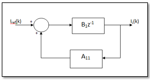 | Figure 5. Block diagram of current loop control for inverter |
Now considering the closed loop control as shown in fig.6, the closed loop transfer function C(z) is given by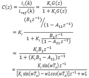 | (18) |
 | Figure 6. Closed loop current control for inverter |
The discrete time model of voltage loop control is shown in fig.7. 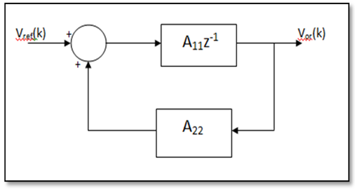 | Figure 7. Open loop voltage control for inverter |
The transfer function G(z) is given as:-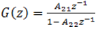 | (19) |
Considering the open loop transfer function the model of closed loop voltage control is shown in fig.8.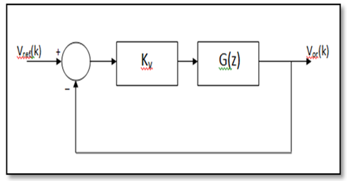 | Figure 8. Closed loop voltage control for inverter |
The transfer function of closed loop voltage control C (z) is given as | (20) |
Based on the equation derived for the closed loop current control and voltage control, an algorithm is developed for generation of PWM signal for each phase.
6. Simulation Model of PWM Inverter
Figure 9 shows the simulation model of PID controlled 5KVA three phase PWM inverter with PV source [12]. This model is build using six IGBT along with six anti-parallel diodes in simulink. IGBT has internal resistance Ron=0.01Ω, snubber resistance Rs =1KΩ, KP=0.4 and Ki=500. In the model, sinusoidal wave at 50-Hz and carrier frequency of 1080Hz are compared to generated PWM signals. The nonlinear load has following parameters: the inductance and capacitance of the filter is 10mH and 110µF respectively. Nominal frequency 50Hz, active power 3KW, inductive reactance power 100W and capacitive reactance power 100W. 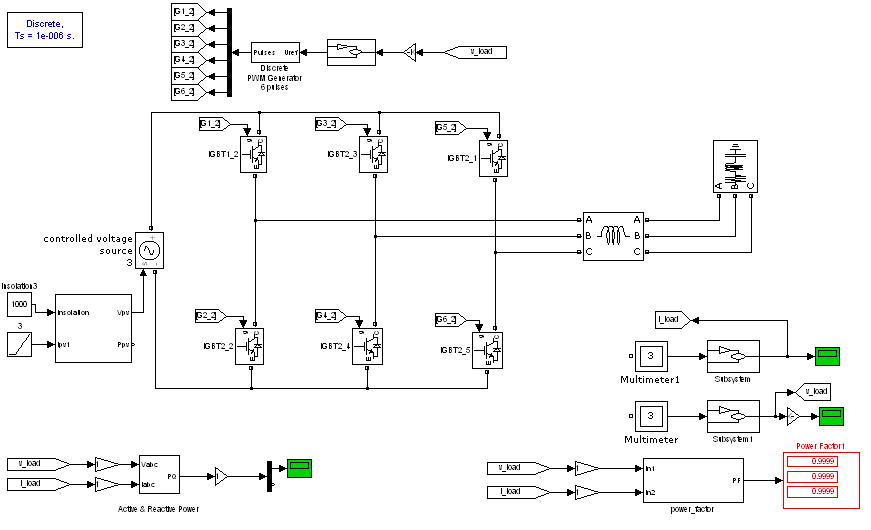 | Figure 9. Simulation model of PWM inverter |
7. Code Composer Studio (IDE)
Code Composer Studio (CCS) is the environment for project development and for all tools needed to build an application for the DSP. The objective of this module is to understand the basic functions of the Code Composer Studio Integrated Design Environment for the C2000 - Family of Texas Instruments Digital Signal Processors. This involves understanding the basic structure of a project in C and Assembler -coded source files, along with the basic operation of the C-Compiler, Assembler and Linker. The core is the TMS320F2812 32-bit DSP on board of Spectrum Digital’seZdspF2812. All the internal peripherals are available through connectors. The on board JTAG – emulator connected to the PC using a parallel printer cable.
8. Running the Software
The Matlab model for generation of PWM signal has been developed for 30 KVA three phase PWM inverter system as shown in figure 10. It consists of three sine wave block, C28Xpwm and F2812eZdsp board. After running this model in CCS, DSP generate the PWM signal as shown in figure 13. 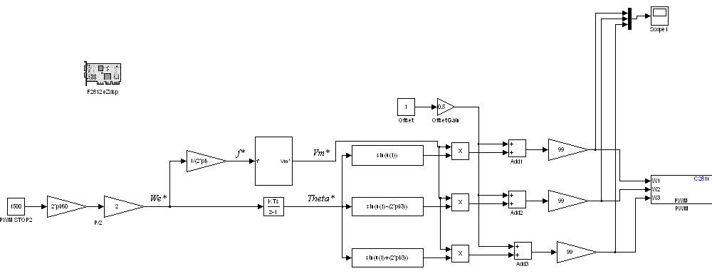 | Figure 10. Matlab/Simulink model of PWM generation |
The equation (3), (4) and (5) based on the amplitude Vm and the phases that is 0, 120 and 240 degree were considered. Comparing the combined effect of each block, the generated signal was applied to PWM generator for generating PWM signal for each phase. The PWM1, PWM3 and PWM5 control logic are active low. The PWM2, PWM4 and PWM6 control logic are active high. After successfully running the Matlab/Simulink model of PWM signal, the model was converted into a project using incremental build option of code composer studio. This project was complied and builds to run for PWM signal using DSP2812. The generated PWM signal shown in figure 13 through DSP2812 was then applied to the inverter module shown in figure 11. The respective waveform and readings was observed as shown in figure 14, 15 and 16.
9. Hardware Description
Figure 11 shows DSP controlled 30 KVA three phase PWM inverter. The experimental setup is composed of PC, DSP kit, IGBT driver circuit, three phase PWM inverter circuit, inductive load and DSO. In control circuit section, 1MBH50D-060 coded IGBTs are used in PWM inverter circuit. IGBTs are voltage controlled devices and it requires a minimum gate threshold voltage of about 15-V for establishing the rated collector-to-emitter conduction. This requirement makes it difficult to directly interface an IGBT to DSP. For proper operation of IGBTs, correct power levels are required (Vge(th)=15 V and Ic= 50 mA). Voltage and current levels of DSP output signals fail to operate the IGBTs. IGBT driver circuit amplifies DSP output signal to the required level for triggering the IGBTs and isolates the DSP from the power circuit. By varying the speed of motor the load voltage and current as shown in figure 14. The power factor, KVA and KVAR are observed at different load and shown in figure 15. THD is shown in figure 16.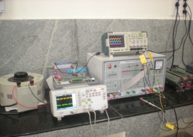 | Figure 11. Experimental setup |
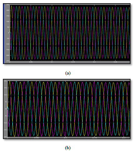 | Figure 12. (a) Load voltage (b) Load current |
10. Results
For MATLAB/SIMULINK model of PID controlled 5KVA three phase PWM inverter, the load voltage and current are observed as shown in figure 12. For the development of hardware model, PWM generation has been done using code composer studio and DSP 2812. Figure 13 shows the generated PWM signal.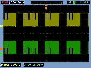 | Figure 13. PWM signal from simulink model using DSP |
After generating the PWM signal by using DSP, it was applied to the developed hardware of 30 KVA three phase inverter. The generated waveforms of load voltage and current are as shown in figure 14.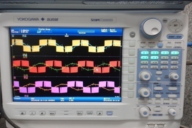 | Figure 14. Load voltage and current of PWM inverter |
The developed model was also tested for its rated power.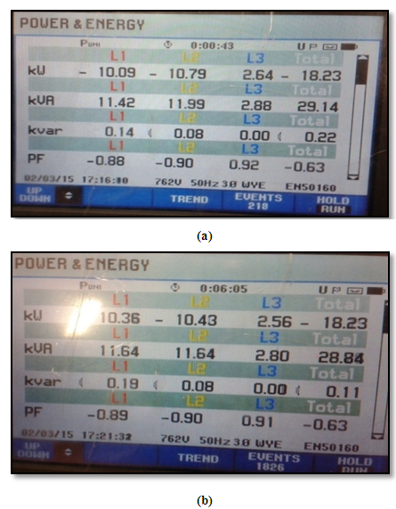 | Figure 15. (a) and (b) Readings of PF,KVA and KVAR |
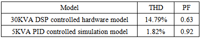
After successfully running the developed hardware, the total harmonics distortion for the simulated model as well as hardware model was measured and compared.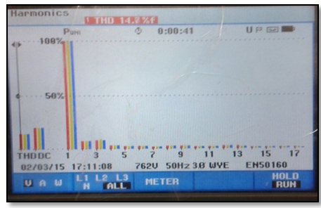 | Figure 16. THD of developed model |
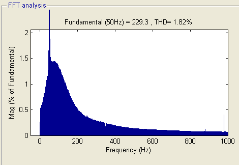 | Figure 17. THD of simulation model |
Table 1. Comparison of THD and PF for the models
 |
| |
|
11. Conclusions
In this paper a MATLAB/ SIMULINK model for three phase 5KVA PID controlled inverter is developed and simulated. The values for generated load voltage and current are 240 volts and 21amp respectively. Based on the simulated result the hardware model for 30 KVA three phase inverter is developed. The PWM signal is generated using DSP 2812. The load voltage and current is found to be 500 volts and 25 amps respectively. The THD and PF is also measured and compared. The THD for the simulated model and hardware model is found to be well below 5% as per IEEE standard. The PF for the simulated model and hardware model is found near one.Thus this paper presents the analysis and design of a digitally controlled three phase PWM inverter to develop more theoretical and practical knowledge on DSP based control application. The algorithm to generate sine modulated PWM signals for three phase inverter using TMS320F2812 DSP is presented. After running the hardware it has been observed that the power factor of each phase is sufficiently maintained and the variation of KVA and KVAR are noted. It is found that KVAR is minimized. The THD and PF for the developed system as well as the Matlab/simulink model have been compared.
ACKNOWLEDGEMENTS
The authors gratefully acknowledge the electrical department of National Institute of Technology, Raipur, India for the cooperation for using the Advanced Power Electronics, Drives and Digital Controller laboratory facility.
References
| [1] | Julien Hobraiche, Jean-Paul Vilain, Patrice Macret, “ A new PWM strategy to reduce the inverter input current ripples”, IEEE transaction on Power Electronics, Vol 24, No. 1, pp 172-180, Jan 2009. |
| [2] | M. F. N. Tajuddin, N. H. Ghazali, I. Daut and B. Ismail, “using DSP technology for true sine PWM inverters”, 27th International Spring Seminar on Electronics Echnology, IEEE, pg 141-146, 2004. |
| [3] | Tamás Kerekes, Dezső Séra, Remus Teodorescu “PV inverter control using a TMS320F2812 DSP”, Proceedings of EDERS 2006, Munich, Germany, April 2006. |
| [4] | Texas Instruments Incorporated, “Implementation of PID and Deadbeat Controllers with the TMS320 Family”, APPLICATION PORT: SPRA083. |
| [5] | Texas Instruments Incorporated,” TMS320F2810– TMS3202812 Digital Signal Processors Data Manual”. |
| [6] | “TMS320C28X DSP CPU and Instruction Set Reference Guide “Texas Instruments Corporation. |
| [7] | “TMS320F28X DSP Peripherals Reference Guide “Texas Instruments Corporation. |
| [8] | Prashant V. Thakre, Saroj Rangnekar, “Implementation of Digital Signal Controller TMS320C28027 Based PWM for A Single Phase Bidirectional High Frequency Link Photovoltaic Inverter “International Journal of Energy Engineering 2012, 2(2): 15-22. |
| [9] | Zainal Salam, Tohleong Soon, Mohd. Zulkifli Ramli, “Hardware Implementation of high frequency link inverter using dSPACE DS1104 digital signal processing board’ , First IEEE International Conference on Power and Energy Conference PECon, Malaysia, 348- 352, Nov 2006. |
| [10] | Zhao Qinglin, Xu Yunhua, Jin Xiaoyi, Wu Weiyang, “DSP based closed loop control of bidirectional high frequency link inverter with active clamp”, IAS2005, IEEE proceedings, pp 928-933, 2005. |
| [11] | Koutroulis, E., Chatzakis, J. Kalaitzakis, K. and Voulgaris, N. C. A “Bidirectional, Sinusoidal, High-Frequency Inverter Design”, IEEE Proceedings on Electric Power Applications, 2001, 148(4): pp 315-321. |
| [12] | Deshmukh V.M., Patil A.J. “Comparison and performance analysis of closed loop controlled nonlinear system connected PWM inverter based on hybrid technique”JESIT, ELSEVIER, volume 2(2015) PP 86-98. |
 Abstract
 Reference
 Full-Text PDF
 Full-text HTML