S. Tasouji Hassanpour 1, A. Arjhangmehr 2, S. A. H. Feghhi 2, E. Mostafapour 3
1Department of Industrial Eng. , K.N Toosi University of Technology, Tehran, Iran
2Department of Nuclear Eng. , Shahid Beheshti University G.C., Tehran, Iran
3Department of Communication Eng. , Faculty of technical and engineering of Urmia University, Urmia, Iran
Correspondence to: S. Tasouji Hassanpour , Department of Industrial Eng. , K.N Toosi University of Technology, Tehran, Iran.
| Email: |  |
Copyright © 2014 Scientific & Academic Publishing. All Rights Reserved.
Abstract
Nowadays, multilevel converters are a good solution for power applications regarding the fact that they can obtain high power using mature medium-power semiconductor technology. Among three types of inverter topologies, cascaded multilevel inverter reaches the higher output voltage and power levels (13.8 kV, 30 MVA), and the higher reliability due to its modular topology. Although multi-level inverters generate low harmonic distortion, the output voltage waveform is not accurately a sinusoidal wave. Minimization of total harmonic distortion (THD) is one of the objectives of inverter field researches. On the other hand, reduction of construction costs is the other purposes of power electronics engineering issues. This could be achieved by reduction of some elements of the circuit. Therefore, this paper tries to combine two techniques in order to accomplish better cascade multi-level inverter. First technique produces more voltage steps with less number of DC sources and less number of switches. Second one tries to set the optimum values for DC sources and subsequently voltage steps through Fourier analysis. Finally, techniques would be compared.
Keywords:
Cascade Multi-Level Inverter, H-Bridge, Optimum Voltage Levels, DC Sources, Total Harmonic Distortion
Cite this paper: S. Tasouji Hassanpour , A. Arjhangmehr , S. A. H. Feghhi , E. Mostafapour , THD Minimization in Cascade Multi-level Inverters with a Few DC Sources and Optimum Voltage Levels, International Journal of Control Science and Engineering, Vol. 3 No. 2, 2013, pp. 58-67. doi: 10.5923/j.control.20130302.04.
1. Introduction
Application of power electronics in power systems are growing rapidly. In distributed generation, power electronics is needed to interface non-conventional energy sources such as wind, photovoltaic, and fuel cells to the utility grid. In photovoltaic systems, solar cells produce dc, with I-V characteristic shown in Figure 1a that requires a power electronics interface to transfer power into utility system, as shown in Figure 1b.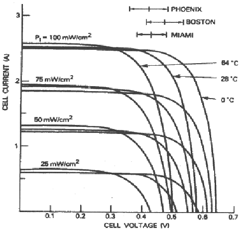 | Figure 1a. I-V characteristic of solar cell |
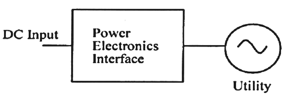 | Figure 1b. Transferring power to utility by the means of power electronics |
Use of power electronics allows control over the flow of power on transmission lines, an attribute that is especially significant in a deregulated utility environment. Also, the security and the efficiency aspects of power systems operation necessitate increased use of power electronics in utility applications [1]. The term multilevel began with the three level converters [2]. Later, several multilevel converter topologies have been developed [3–6]. In 1998 Manjrekar has proposed a cascade topology that uses multiple dc levels, which instead of being identical in value are multiples of each other [7, 8]. He also uses a combination of fundamental frequency switching for some of the levels and PWM switching for part of the levels to achieve the output voltage waveform. This approach enables a wider diversity of output voltage magnitudes; however, it also results in unequal voltage and current ratings for each of the levels and loses the advantage of being able to use identical modular units for each level.The main advantages and disadvantages of multilevel cascaded H-bridge converters are as follows [9, 10].Advantages:The number of possible output voltage levels is more than twice the number of dc sources (m = 2s + 1).• The series of H-bridges makes for modularized layoutand packaging. This will enable the manufacturing process to be done more quickly and cheaply.Disadvantages:• Separate dc sources are required for each of the H-bridges. This will limit its application to products that already have multiple SDCSs readily available.
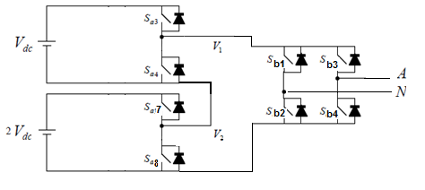
2. First Technique: More Voltage Steps Using Less DC Sources and Switches
Each H-bridge connected to  volts DC source, could generate three voltage levels:
  , 0, and -
 . Beside, each decimal number could be converted into binary number. For instance, to count from zero to seven, 3 binary digits would be required. Below illustration shows that how a decimal number (6) is produced by three digits in binary system. Another word, below illustration shows that how a decimal voltage step (6) is produced by three DC sources.
 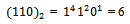 | (1) |
Above phrase shows that, there is no need to use six separate volatge sources to produce 6-level inverter. To produce step sixth, according to above phrase, three different voltage sources would be needed. Voltage sources should have values equal to powers of 2: | (2) |
 | (3) |
 | (4) |
To generate step sixth, the H-bridge connected to  should produce 0 volts. The H-bridge connected to
  should produce
  volts and The H-bridge connected to
  should produce
  volts. Then the output voltage would be equal to
  . Using this technique,
  steps is produced by
  DC sources, as shown in Figure 2.Another advantage of this technique is to use less switches. If the condition of a switch in a whole period doesn’t change, it could be replaced with a open circuit or a short circuit (according to switch’s condition). Additionally, it is possible to reduce the duty cycle of circuit by one H-bridge module. It means that, if one can produce the positive (negative) part of sinusoidal wave and apply it to the input of H-bridge module, then it is possible to generate the negative (positive) part of sinusoidal wave in the final output terminals. New form of multi-level cascade invereter for producing 3-levels is shown in Figure 3. As it is obviuse in Figure 3, for two H-bridge configuration the number of switches doesn’t change. But as the number of H-bridge blockes increases the number of switches could be decreases in comparision with standard multi-level configuration.
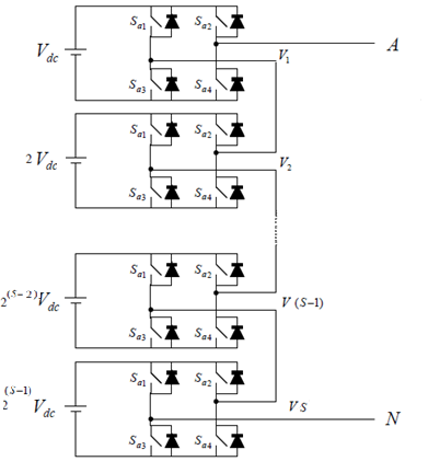 | Figure 2. Cascade mult-level invereter with few DC sources and more voltage steps |
 | Figure 3. New configuration of switchecs in multi-level inverter |
If  stands for number of H-bridge blocks and
  stands for number of used switches, then:
 | (5) |
 | (6) |
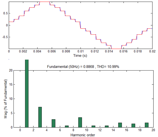
Using this technique the total harmonic distortion for three and seven steps are simulated and calculated.Figure 4 shows that using this technique leads to produce 16.53% total harmonic distortion for 3-level inverter. Figure 7 illustrates that using only three DC source could produce 7-level inverter and it generates THD about 10.98%.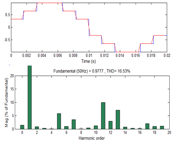 | Figure 4. Signal and FFT analysis for 3-level inverter using only two DC sources |
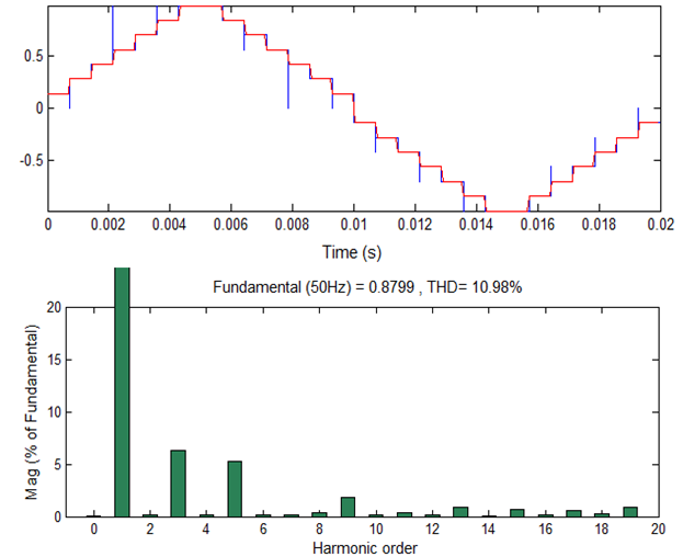 | Figure 5. Signal and FFT analysis for 7-level inverter using only three DC sources |
3. Second Technique: Optimum Voltage Levels
By writing Fourier series for the output signal of a cascade inverter one can find the harmonic orders equation. Coefficients of odd components of Fourier series are the harmonic orders. Fourier series equation is: | (1) |
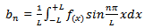 | (2) |
Fourier series for the output voltage of 2-level inverter which is shown in Figure 6 has been written, the coefficient of sinusoidal components is: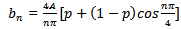 | (3) |
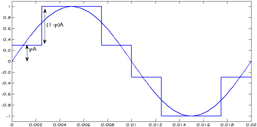
Where  is the amplitude of fundamental sin wave or summation of DC voltage sources.
  is a percentage of amplitude which is occurs in first step.
  shows the value of first step. On the other word
  determines the value of first DC voltage source in a 2-level inverter.
  is the number of harmonic order.For 3-level inverter
  is equal to:
 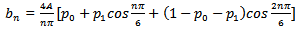 | (4) |
Where  and
and  show the values of first and second steps, respectively. By the help of principle of mathematical induction one can write the equation for amplitude of harmonics for k-level inverter:
 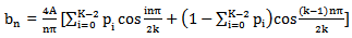 | (5) |
Where,  are the values for each voltage level. The total harmonic distortion equation could be written as follows:
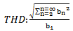 | (6) |
Equation (5) will helps to calculate the  values rapidly. So there is no need to write the Fourier series for finding
  values. Equations (5) and (6) help to determine the optimum value of voltage levels. To find the optimum value of levels we should answer this question:Which values of
  will minimize equation (6)?It is clear that:
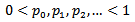 | (7) |
 | (8) |
Objective function which should be optimum is a multi-variable function. When multi level inverter has  steps the objective function has
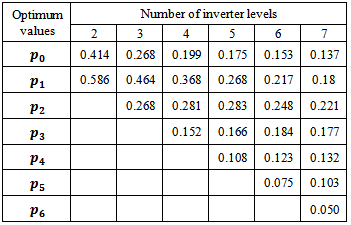
  variables. For optimization process MATLAB software has been used. To obtain steps values, constrained nonlinear minimization method has been used. If only
  , and
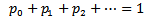
, and  have been considered, values shown in Table.1 are the optimum ones.
 Table 1. Optimum values for voltage levels (DC sources)
 |
| |
|
 | Figure 6. Output voltage of 2-level inverter and its fundamental sin wave |
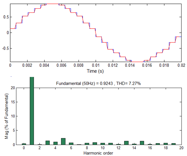
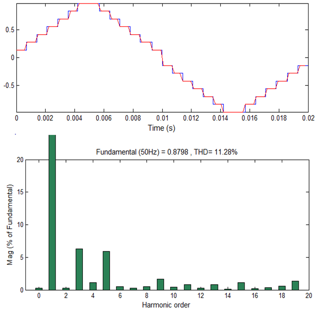
For second technique, simulation process for 3 and 7 levels have been performed. Results are shwon in figures 7 and 8. With optimum DC sources, THD decreases to 15.59% for 3-level and 7.27% for 7-level. 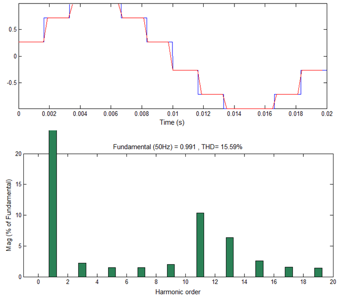 | Figure 7. Signal and FFT analysis for 3-level inverter using optimum DC sources |
 | Figure 8. Signal and FFT analysis for 7-level inverter using optimum DC sources |
4. Third Technique: Combination of First and Second Techniques
In order to achieve better sinusoidal wave form in the output of cascade multi-level inverter, two previous techniques are combined.Additionally, this combination technique provides low costs due to few usage of sources and swithches. Number of DC sources determines the variables of objective function in minimization procedure. As an example, to minimize the THD in 7-level multi level, there exists three variables: V(1), V(2), and V(3). Objective function for 7-level inverter could be written as follows:Function THD= func7(v)b1=v(1)+(v(2)-v(1))*cos(pi/14)+v(1)*cos(2*pi/14)+(v(3)-v(2)-v(1))*cos(3*pi/14)+v(1)*cos(4*pi/14)+(v(2)-v(1))*cos(5*pi/14)+(1-v(2)-v(3))*cos(6*pi/14);b3=(v(1)+(v(2)-v(1))*cos(3*pi/14)+v(1)*cos(6*pi/14)+(v(3)-v(2)-v(1))*cos(9*pi/14)+v(1)*cos(12*pi/14)+(v(2)-v(1))*cos(15*pi/14)+(1-v(2)-v(3))*cos(18*pi/14))/3;b5=(v(1)+(v(2)-v(1))*cos(5*pi/14)+v(1)*cos(10*pi/14)+(v(3)-v(2)-v(1))*cos(15*pi/14)+v(1)*cos(20*pi/14)+(v(2)-v(1))*cos(25*pi/14)+(1-v(2)-v(3))*cos(30*pi/14))/5;b7=(v(1)+(v(2)-v(1))*cos(7*pi/14)+v(1)*cos(14*pi/14)+(v(3)-v(2)-v(1))*cos(21*pi/14)+v(1)*cos(28*pi/14)+(v(2)-v(1))*cos(35*pi/14)+(1-v(2)-v(3))*cos(42*pi/14))/7;THD=sqrt(b3^2+b5^2+b7^2)/b1;Results of minimization for 3 and 7-level inverters shows that the optimum values of DC sources are:For 3-level inverter:  For 7-level inverter:
  Simulation process have done by the use of this optimum values in MATLAB software. Switching frequency of combined technique is equal to: number of levels × 100 Hz. Figure 9 and Figure 10 show signal and FFT analysis for combined technique.
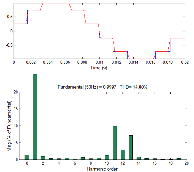 | Figure 9. Signal and FFT analysis for 3-level inverter using combined technique |
 | Figure 10. Signal and FFT analysis for 7-level inverter using combined technique |
For 3-level the THD reduces about 1.73% and 0.79% in comparison to first and second techniques, respectively. THD in this case is equal to 14.80%. For 7-level THD is equal to 10.99%. this value is bigger than THD of second technique but it is approximately equal to THD of first technique.
5. Forth Technique: Standard Cascade Multi-Level Inveretr
This section reviews the standard multi-level inverter so as to compare with introduced techniques. In standard conventional multi-level inverter, DC sources are equal and output voltage level is the same to number of DC sources. Figure 11 shows the standard cascade multi-level inverter.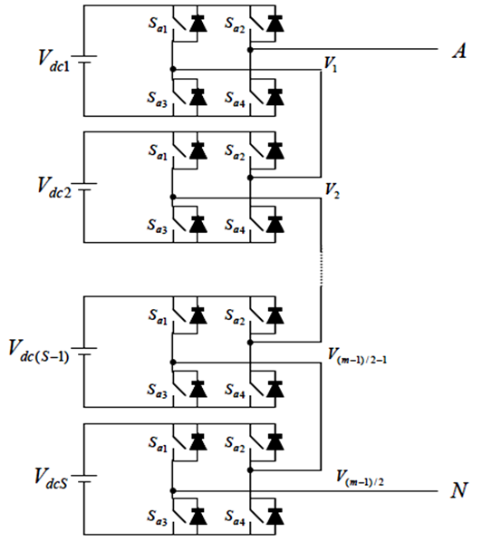 | Figure 11. Standard cascade multi-level inverter |
Signal and FFT analysis of 3 and 7-level standard multi-level has been performed and the rresults are shown in Figure 12 and 13, respectively. 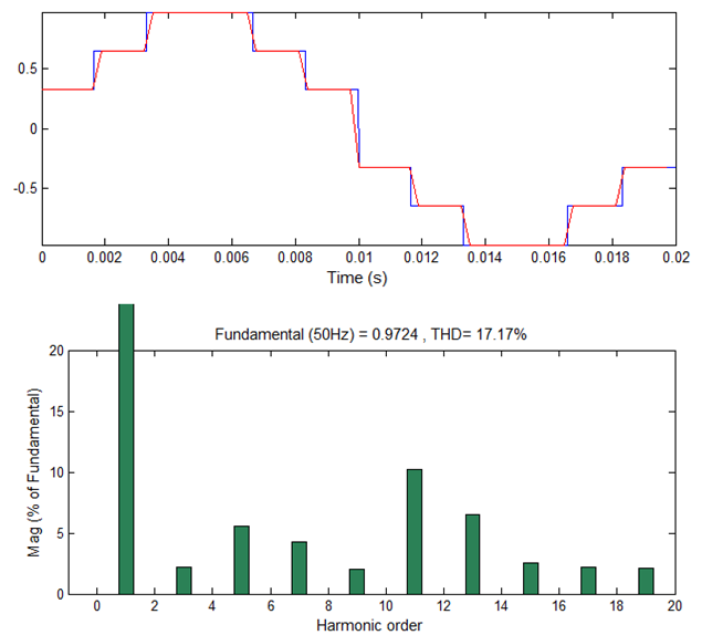 | Figure 12. Signal and FFT analysis for 3-level inverter using standard technique |
 | Figure 13. Signal and FFT analysis for 7-level inverter using standard technique |
It could be seen that the THD in standard case is higher than other techniques.
6. Comparison
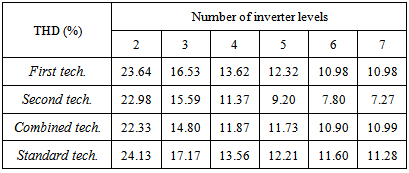
This section summerizes the features of four techniques in table.2 and table.3.Table 2. THD values for differenr techniques
 |
| |
|
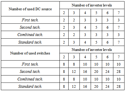
Table 3. Used DC sources and switches in different techniques
 |
| |
|
According to table.2 second technique provides less THD than the others. Consequently, in cases that the main object is to acheive less THD, this technique should be used.
7. Conclusions
This paper has successfully demonstrated some techniques in cascade multi-level inverters in order to achieve low costs and less total harmonic distortion. Although combined technique provides less number of switches and DC sources but watt usage in all techniques would be equal. Another word, costs would reduce in first and combined techniques because as the power in a DC source increases, per power cost would decrease. Therefore, it is better to use a 1 watt, a 2 watts, and a 4 watts DC sources instead of using seven 1 watt DC sources. Features of combined technique could be named as follows:1) Low construction costs2) Less THD due to optimum DC sourcesOptimum values are gained in minimization process, were not round values. Available DC sources such as photovoltaic panels have round voltage values. Thus, for practically design and built a low harmonic and low cost cascade multi-level inverter, optimum DC source values in combined technique should cut or round. This could be a part of our future works.
References
| [1] | N. Mohan, “First course on power electronics and drives”, edition, MNPERE, Minneapolis, 2003 |
| [2] | A. Nabae, I. Takahashi, and H. Akagi, “A New Neutral-point Clamped PWM Inverter,” IEEE Transactions on Industry Applications, vol. IA-17, Sept./Oct. 1981, pp. 518–523. |
| [3] | F. Z. Peng and J. S. Lai, “Multilevel Cascade Voltage-source Inverter with Separate DC Source,” U.S. Patent 5 642 275, June 24, 1997. |
| [4] | P. W. Hammond, “Four-quadrant AC-AC Drive and Method,” U.S. Patent 6 166 513, Dec. 2000. |
| [5] | M. F. Aiello, P. W. Hammond, and M. Rastogi, “Modular Multi-level Adjustable Supply with Series Connected Active Inputs,” U.S. Patent 6 236 580, May 2001. |
| [6] | M. F. Aiello, P. W. Hammond, and M. Rastogi, “Modular Multi-Level Adjustable Supply with Parallel Connected Active Inputs,” U.S. Patent 6 301 130, Oct. 2001. |
| [7] | M. D. Manjrekar and T. A. Lipo, “A Hybrid Multilevel Inverter Topology for Drive Applications,” IEEE Applied Power Electronics Conference, 1998, pp. 523–529. |
| [8] | M. D. Manjrekar and T. A. Lipo, “A Generalized Structure of Multilevel Power Converter,” IEEE Conference on Power Electronics, Drives, and Energy Systems, 1998, Australia, pp. 62 67. |
| [9] | C. Hochgraf, R. Lasseter, D. Divan, and T. A. Lipo, “Comparison of Multilevel Inverters for Static Var Compensation,” Conference Record – IEEE Industry Applications Society 29th Annual Meeting, 1994, pp. 921–928. |
| [10] | J. S. Lai and F. Z. Peng, “Multilevel Converters – A New Breed of Power Converters,” IEEE Transactions on Industry Applications, vol. 32, no. 3, May 1996, pp. 509–517. |
 Abstract
 Reference
 Full-Text PDF
 Full-text HTML