-
Paper Information
- Paper Submission
-
Journal Information
- About This Journal
- Editorial Board
- Current Issue
- Archive
- Author Guidelines
- Contact Us
International Journal of Composite Materials
p-ISSN: 2166-479X e-ISSN: 2166-4919
2024; 14(1): 1-4
doi:10.5923/j.cmaterials.20241401.01
Received: Mar. 2, 2024; Accepted: Mar. 16, 2024; Published: Mar. 22, 2024

Ultrasonic Impact on nCdS / pCdTe Heterostructures
 Abstract
 Reference
 Full-Text PDF
 Full-text HTML
Sh. B. Utamuradova 1, S. A. Muzafarova 1, A. S. Achilov 2, M. A. Makhmudov 2, Z. S. Kenzhaeva 1
1Research Institute of Semiconductors Physics and Microelectronics, Yangi Olmazor, 20, Tashkent, Uzbekistan
2Physical-Technical Institute of the Uzbekistan Academy of Sciences, Chingiz Aytmatov Str. 2B, Tashkent, 100084, Uzbekistan
Correspondence to: S. A. Muzafarova , Research Institute of Semiconductors Physics and Microelectronics, Yangi Olmazor, 20, Tashkent, Uzbekistan.
| Email: |  |
Copyright © 2024 The Author(s). Published by Scientific & Academic Publishing.
This work is licensed under the Creative Commons Attribution International License (CC BY).
http://creativecommons.org/licenses/by/4.0/

The intermediate layer of the ternary compound (CdTe1-x Sx) interface, formed at the heterointerface of the nCdS/pCdTe structure, using the photoelectric method was studied. Band gap of CdTe1-x Sx solid solution was determined from the fundamental intrinsic absorption edge data. It has been shown that at substrate temperatures Tn ≈ 220-240°C, along with stable ones, metastable compounds CdTe1-x Sx are formed, which are annealed after ultrasonic irradiation with a power of 1 W/ cm2 for 10 minutes. For the CdTe1-x Sx layer, the composition (x) and crystal lattice constants a0(x) were calculated on the nCdS / pCdTe photoconductivity spectrum.
Keywords: Heterojunction, Solid solution, Photoelectric, Composition, Spectrum, Photosensitivity
Cite this paper: Sh. B. Utamuradova , S. A. Muzafarova , A. S. Achilov , M. A. Makhmudov , Z. S. Kenzhaeva , Ultrasonic Impact on nCdS / pCdTe Heterostructures, International Journal of Composite Materials, Vol. 14 No. 1, 2024, pp. 1-4. doi: 10.5923/j.cmaterials.20241401.01.
1. Introduction
- In recent years, many authors have conducted research [1,2] on the development of solar cells (SCs) based on polycrystalline pCdTe films with an nCdS / pCdTe heterostructure (HS) and have shown that such SCs have great promise for solar energy.Therefore, much attention is paid to technological methods for creating nCdS / pCdTe HSs and the study of electronic processes in such structures. It has been established that during the growth of the nCdS / pCdTe structure, a thin layer is formed at the heterointerface between the CdS and CdTe films. Recent specially conducted experimental studies of nCdS / pCdTe HS using the NSOM method (near - field scanning optical microscopy) showed [3-5] that a transition intermediate layer is formed due to the diffusion of sulfur from CdS into CdTe under certain technological conditions, resulting in the formation of a solid solution (SS) CdSx Te1- x.The authors of [6,7] showed that semiconductor binary compounds CdS and CdTe, interacting with each other, form a solid solution type CdSx Te1-x with a continuous composition x (0< x <1). The efficiency of nCdS / pCdTe solar cells is largely determined by the perfection of the composition of the solid solution structure and its geometric dimensions and phases [7]. Ensuring continuity of the CdSxTe1-x solid solution [6] at the heterointerface creates a favorable effect. The band gap of the HS increases towards the irradiated surface; the built-in electric field, caused by the gradient of the band gap Eg, leads to the retraction of minority carriers into the bulk of the films to a depth significantly exceeding the diffusion length. As a result, surface recombination is reduced, and the value of the minority charge carrier collection coefficient is relatively high, close to unity over a wide photosensitivity region. The decline in photosensitivity in the short-wavelength region of the spectrum is determined by the thickness of the TP layer and the photon energy, starting from which absorption in the wide-bandgap becomes significant n – layer on the surface of the structure.This requires a solid solution CdSx Te1- x with a continuous composition x thickness of the order of 1 μ m, where the value of x should vary from cadmium sulfide to cadmium telluride. The use of high-temperature technology for the formation of nCdS / pCdTe HS leads to an increase in the content of uncontrolled impurities throughout the structure, including in the CdTe film. Therefore, it is of great interest to study nCdS / pCdTe HSs within the range of formation temperatures at which the properties of thin CdTe films remain almost unchanged.As is known, ultrasound waves (US) affect the defect structure and electrical characteristics of semiconductors and semiconductor structures. Effects with ultrasonic influence appear in areas of semiconductor structures where an internal stress field is observed. Such fields are a factor contributing to the formation and recombination of defects under the influence of ultrasound. It is of great interest to study the influence of ultrasonic influence on the interface GS nCdS / pCdTe and study of the presence of a transition layer of the interface between nCdS and pCdTe [5].
2. Methodology and Experiment
- The formation of a solid solution at a heterointerface has been studied nCdS / pCdTe solar cells depending on the technological mode and the subsequent stimulating factor - ultrasonic influence (US). nCdS / pCdTe SCs with an area of 1 cm2 were manufactured by the authors using technology [8] on a molybdenum substrate. CdTe/CdS heterojunctions with an area of 1 cm2 were manufactured using the technology described in [2]. The front contact, from which the illumination is carried out, is made of indium deposited in a vacuum of ~10 -5 Torr in the form of a comb. In this case, the width of the contact strip was 0.8 mm, and the distance between the strips was ~2 mm. The rear contact is made of molybdenum. The composition of the CdTe/ CdS interface was studied by X-ray microprobe analysis using the Kameka unit. For this purpose, an oblique grind of CdS / CdTe structures was carried out at an angle of 1.5°. The analysis was carried out at points every 25 μm, which corresponds to a movement in depth by a step of 0.65 μm.The front contact, from which the illumination is carried out, is made of pure indium (In), deposited in a vacuum of 10 -5 torr in the form of a comb, where the width of the contact strip is 0.8 mm, the distance between the strips is 2 mm. Molybdenum foil served as the rear contact.The spectral dependence of photosensitivity was measured on a ZMR-2 monochromator at room temperature. The source of radiation was a xenon lamp of the DKSSh-1000 type, operating in the mode of the minimum permissible power for the luminous flux of 53,000 lm, with a brightness of up to 120 Mcd •m -2 with a central light spot. The radiation is calibrated in absolute units using a thermoelement with a quartz window RTE-9. The samples under study were also subjected to ultrasonic irradiation. Irradiation was carried out at a frequency ν = 2.5 MHz with a power W = (0.5÷ 1) W / cm2 for 10÷15 minutes.The conducted studies show that the phase composition and thickness of the layer of intermediate solid solution strongly depend on the technological regime of HS formation, mainly on the selection of the substrate temperature and the duration of the growth process.
3. Discussion
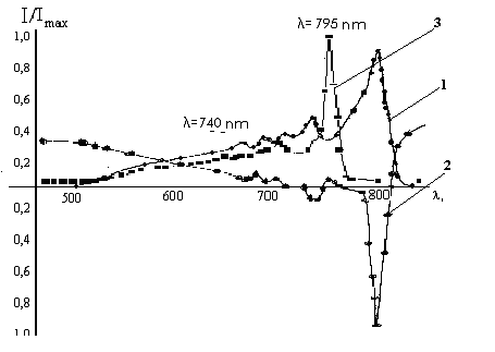
- The intermediate layer CdSx Te1- x begins to form in our technique, at the substrate temperature Tp ≈150°C. It has been experimentally established that with increasing substrate temperature The solid solution CdSx Te1- x begins to be enriched with S atoms and the value of x begins to increase [1,9]. As is known [7,9,10], each composition x SS is characterized by the corresponding value of the lattice constant a0, which are between the lattice constants of CdS (a0 =5.832 Ǻ) and CdTe (a0 =6.423 Ǻ).Figure 1 (curve 1) and Figure 2a (curve 1) show the spectral distribution of photosensitivity of GS and CdS / pCdTe obtained at substrate temperatures Tp = 180°C and Tp = 220°C. In the spectral distribution of photosensitivity between the edges of the intrinsic absorption of CdS and CdTe GS nCdS / pCdTe, obtained at a temperature Tp = 180°C, obvious peaks are observed at λ1 max = 670 nm, λ 2 max = 690 nm, λ 3 max = 740 nm, λ 4 max = 795 nm (Fig. 1, curve 1). After ultrasonic exposure for 10 minutes, the maxima at λ max =670 nm and λ 2 max =690 nm disappear. At the same time, the peak at λ 3 max =740 nm significantly increases in amplitude, and the main peak λ 4 max =795÷797 nm remains practically unchanged (Fig. 1. cr.2). Ultrasound exposure increases the photosensitivity of the structure over the entire spectral range, especially in the spectral region λ =600÷750 nm.
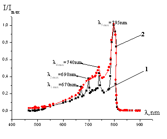 | Figure 1. Spectral distribution of photosensitivity of GS nCdS / pCdTe (Tp =180°C): 1-before, 2-after ultrasound exposure |
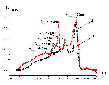 | Figure 2a. Spectral distribution of photosensitivity of GS nCdS / pCdTe (Tp =220°C): 1-before and 2-after ultrasound exposure |
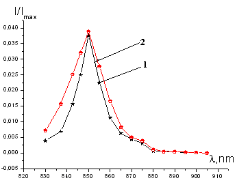 | Figure 2b. Spectral distribution of the long-wave region of the photosensitivity spectrum for nCdS / pCdTe HS (Tp =220°C): 1-before and 2-after ultrasound exposure |
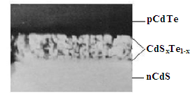 | Figure 3. A microphoto of cross-section section heterojunction nCdS/pCdTe (Тп≥240С) (Increase×1750 .М 1sm 2μm) |
 | Figure 4. Spectral distribution of photosensivity I/Imax(λ) heterojunction nCdS/pCdTe ((Тп=220°C) |
4. Conclusions
- The formation of a solid solution at nCdS / pCdTe heterointerface has been studied, which is formed due to the diffusion of sulfur from CdS into CdTe under certain technological conditions, resulting in the formation of a CdTe1-x Sx solid solution. It has been shown that with increasing substrate temperature, the probability of the formation of a CdTe1- Sx solid solution with different composition increases, as evidenced by the number of peaks in the photosensitivity spectrum. This indicates that the formed layers of the CdTе1-x Sx solid solution the intermediate layer between CdS and CdTe actually differ from each other in composition and electrical properties, as well as geometric dimensions. In summary, we can conclude that at the heterointerface n CdS / p CdTe is formed by SS CdTe1-x Sx of different composition depending on the temperature of the pCdTe substrate during deposition of CdS onto its surface by thermal evaporation in vacuum. In this case, along with stable states, metastable solid states CdTe 1-x Sx are formed, which decay when exposed to ultrasound with a frequency ν = 2.5 MHz with a power W = (0.5÷1) W/cm 2 for 10÷15 minutes. Ultrasonic exposure increases photosensitivity over the entire range of the photosensitivity spectrum in heterostructure samples n CdS / p CdTe obtained at Tp ≥220°C, and in samples obtained at Tn <180°C, photosensitivity increases mainly in the spectral region λ= 610-750 nm.