-
Paper Information
- Previous Paper
- Paper Submission
-
Journal Information
- About This Journal
- Editorial Board
- Current Issue
- Archive
- Author Guidelines
- Contact Us
American Journal of Systems Science
2013; 2(1): 8-12
doi:10.5923/j.ajss.20130201.02
An Effective Data Placement Methodology for Data Dominant Applications Employing ASIP
 Abstract
 Reference
 Full-Text PDF
 Full-text HTML
Srilatha C1, Guru Rao C V2, Prabhu G Benakop3
1Department of ECE, ASTRA, Hyderabad, India, 500008, India
2Department of CSE, SR Engineering College, Warangal, India, 506015, India
3Department of ECE & Principal, ATRI, Hyderabad, India, 500039, India
Correspondence to: Srilatha C, Department of ECE, ASTRA, Hyderabad, India, 500008, India.
| Email: |  |
Copyright © 2012 Scientific & Academic Publishing. All Rights Reserved.
Any embedded system contains both on-chip and off-chip memory modules with different access times. During system integration, the decision to map critical data on to faster memories is crucial. In order to obtain good performance targeting less amounts of memory, the data buffers of the application need to be placed carefully in different types of memory. This data placement problem is addressed with the help of a data dominated embedded application.
Keywords: Memory, Cache, DSP
Cite this paper: Srilatha C, Guru Rao C V, Prabhu G Benakop, An Effective Data Placement Methodology for Data Dominant Applications Employing ASIP, American Journal of Systems Science, Vol. 2 No. 1, 2013, pp. 8-12. doi: 10.5923/j.ajss.20130201.02.
Article Outline
1. Introduction
- Embedded applications are highly performance critical. One of the most critical step in embedded application development flow is system integration, where all the software modules are integrated and mapped to a given target memory architecture. This step has a large performance implication depending on how the memory architecture is used. The memory architecture of embedded DSPs is heterogeneous and contains memories of different types. For example, an embedded system may contain on-chip and off-chip memory modules with different access times, single and dual ported memory, and multiple memory banks to support many simultaneous accesses. During system integration, the decision to map critical data on to faster memories and map non critical data in to slower memories is made. In order to obtain good performance and a reduction in memory stalls, the data buffers of the application need to be placed carefully in different types of memory. This is known as the data placement problem. The hardware designers take the logical memory architecture specification as input and design physical memory architecture. This process is referred as memory allocation in the literature[1]. Each of the logical memories is constructed with one or more memory modules taken from a Semiconductor vendor memory library. For example, a logical memory bank of 16KBX16 can be constructed with four 4KBX16 or eight 2KB X16 or eight 4KBX8 or sixteen 1KBX16 memory units. Each of these options, for different process technology and different memory unit organization results in different performance, area and energy consumption trade-offs. Hence the memory allocation process is performed with the objective to reduce the memory area in terms of silicon gates, and energy consumption. The memory allocation problem in general is NP-Complete. Earlier approaches for the data layout step typically use logical memory architecture as input and as a consequence power consumption data for the memory banks is not available. By considering the physical memory architecture, the data layout method proposed in this chapter can optimize for power as well. Also, a common design assumption in earlier design approaches is that, for data layout, the power and performance are non-conflicting objectives and therefore optimizing performance will also result in lower power. However we show that this assumption in general is not valid for all classes of memory architectures. Specifically, we here show that for DSPs memory architectures, power and performance are conflicting objectives and there is a significant trade-off (up to 70%) possible. Hence this factor needs to be carefully factored in the data layout method to choose an optimal power-performance point in the design space.
2. Previous Work
- Many authors have addressed this data placement problem and mapping of logical memory into physical memory.[2] Presented an interference graph based approach for partitioning variables that are simultaneously accessed in different on chip memory banks.[3] Presented an efficient data partitioning approach for data arrays on limited-memory embedded systems. They perform compile time partitioning of data segments based on the data access frequency. In[4] a data partitioning technique is presented that places data into on-chip SRAM and data cache with the objective of maximizing performance. Based on the life times and access frequencies of array variables, the most conflicting arrays are identified and placed in scratch pad RAM to reduce the conflict misses in the data cache. In dynamic data layout[5], on-chip SPRAM is reused by overlaying many data variables to the same address. Thus, two addresses are assigned to a variable at compile time, namely, load address and run address. In[6], the authors present a heuristic algorithm to efficiently partition the data to avoid parallel conflicts in DSP applications. Their objective is to partition the data into multiple chunks of same size so that they can fit in memory architecture with uniform bank sizes. This approach works well if we consider only performance as an objective. Our work addresses the problem of reducing the memory stalls by efficient data partitioning within the on chip scratch pad RAM itself. Also our work addresses the data layout for DSP applications, where resolving self and parallel conflicts by efficient partitioning of data variables is very critical for achieving real-time performance.
3. Proposed Approach
- Initially, the application's data is grouped in to logical sections. This is done to reduce the number of individual items and there by reduce the complexity. This step is important as once the data is grouped into a section, the section can only be assigned a single location and all the data variables inside a section will be placed contiguously starting from the given memory address. Also the order of data placement within a section can be random and may not affect the performance. Note that, a section cannot have both code and data. There is a trade-off in combining different variables into a section. If too many data variables are combined into one section, then the flexibility of placement in memory gets negatively impacted. On the other hand, if each of the data variable is mapped into one section then there are too many sections to handle and thus increasing the data layout complexity. In practice, however an embedded development engineer makes a judicious choice of mapping a set of data variables into a section. Typically, each of the large data arrays are mapped into an individual section, and all data scalar variables belonging to a module are mapped into a section. Note that this process is performed manually. Once the grouping of data into sections are done, the code is compiled and executed in a cycle accurate software simulator. From the software simulator profile data (access frequency) of data sections are obtained. In addition, the simulator generates a conflict matrix that represents the parallel and self conflicts. Parallel conflicts refers to simultaneous accesses of two different data sections while self conflicts refers to simultaneous accesses of same data sections. Consider the following code:
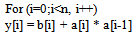 In this code segment data sections a and b need to be accessed together and therefore represent a parallel conflict. Accesses to a[i] and a[i-1] refer to a self conflict. If these arrays (a,b) is placed in different memory banks or memory bank with multiple ports then these accesses can be made concurrently without incurring additional stall cycles. However, note that the data array (a) which has a self conflict must be placed in a memory bank with multiple ports to avoid additional stall cycles. The conflict relations among data sections is represented by an nXn matrix, where n is the number of data sections. The (i; j)th element represents the conflict or concurrent accesses between data section i and j. The diagonal elements represent self conflicts. The conflict matrix is symmetric. As an example, consider an application with 4 data sections: a, b, c and d. A conflict matrix is shown below, where the indices i and j are ordered as a, b, c and d. Section a conflicts with itself and sections b and d. In this matrix, more specifically, a conflicts with itself 100 times, while it conflicts with b and d 40 and 2000 times respectively. The sums of all the conflicts for data sections a, b, c, and d are 2140, 540, 650 and 2050 respectively. Hence the sorted order of the data sections in terms of total conflicts is a, d, c, b.
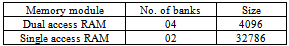
  Data section sizes, access frequency of data sections, conflict matrix and the memory architecture are given as inputs to data layout. The objective of data layout is to efficiently use the memory architecture by placing the most critical data section in on-chip RAM and reduce bank-conflicts by placing conflicting data in different memory banks. Data layout assigns memory addresses for all the data sections. Consider a memory architecture M with m on-chip SARAM memory banks, n on-chip DARAM memory banks, and an off-chip memory. The size of each of the on-chip memory bank and the off-chip memory is fixed. The access time for the on-chip memory banks is one cycle, while that for the off-chip memory is l cycles. Given an application with d sections, the simultaneous access requirement of multiple arrays is captured by means of a two dimensional matrix C where Cij represents the number of times data sections i and j are accessed together in the same cycle in the execution of the entire program. We do not consider more than two simultaneous accesses, as the embedded core typically supports up to two accesses in a single cycle. If data sections i and j are placed in two different memory banks, then these conflicting accesses can be satisfied simultaneously without incurring stall cycles. Cii represents the number of times two accesses to data section I are made in the same cycle. Self-conflicting data sections need to be placed in DARAM memory banks, if available, to avoid stalls. The objective of the data placement problem is to place the data sections in memory modules such that the following are minimized: 1. Number of memory stalls incurred due to conflicting accesses of data sections placed in the same memory bank 2. Self-conflicting accesses placed in SARAM banks 3. Number of off-chip memory accesses. Genetic Algorithm For Data PlacementWe formulate the data layout problem as a multi objective GA[30] to obtain a set of optimal design points. The multiple objectives are minimizing memory stall cycles and memory power. The logical memory architecture contains the number of memory banks, memory bank sizes, memory bank types (single- port, dual-port), and memory bank latencies. The logical memory to physical memory map is obtained using a greedy heuristic method which is explained in the following section. The data placement problem is herewith addressed as a Genetic Algorithm (GA). The data layout block takes the application data and the logical memory architecture as input and outputs a data placement. The cost of data placement in terms of memory stalls is computed. To compute the memory power, we use the physical memory architecture and use the power per read/write obtained from the ASIC memory library. Based on the fitness function, the GA evolves by selecting the fittest individuals (the data placements with the lowest cost) to the next generation. To handle multiple objectives, the fitness function is computed by ranking the chromosomes based on the non-dominated criteria). This process is repeated for a maximum number of generations specified as a input parameter. Mapping Logical Memory to Physical Memory To get the memory power and area numbers, the logical memories have to be mapped to physical memory modules available in a ASIC memory library for a speci¯c technology/process node. As mentioned earlier each of the logical memory bank can be implemented physically in many ways. For example, for a logical memory bank of 4K*16 bits can be formed with two physical memories of size 2K*16 bits or four physical memories of size 2K*8 bits. Di®erent approaches have been proposed for mapping logical memory to physical memories. The memory mapping problem in general is NP-Complete. However since the logical memory architecture is already organized as multiple memory banks; most of the mapping turns out to be a direct one to one mapping. In this chapter a simple greedy heuristic is used to perform the mapping of logical to physical memory with the objective of reducing silicon area. This is achieved by firrst sorting the memory modules based on area/byte and then by choosing the smallest area/byte physical memory to form the required logical memory bank size. Though this heuristic is very simple, it results in efficient physical memory architecture. Genetic Algorithm FormulationTo map the data layout problem to the GA framework, we use the chromosomal representation, fitness computation, selection function and genetic operators. For easy reference and completeness, we briefly describe them in the following sub-sections. Chromosome Representation For the data memory layout problem, each individual chromosome represents a memory placement. A chromosome is a vector of d elements, where d is the number of data sections. Each element of a chromosome can take a value in (0.. m), where 1..m represent on- chip logical memory banks (including both SARAM and DARAM memory banks) and 0 represents off-chip memory. For the purpose of data layout it is sufficient to consider the logical memory architecture from which the number of memory stalls can be computed. However, for computing the power consumption for a given placement done by data layout, the corresponding physical memory architecture obtained from our heuristic mapping algorithm, need to be considered. Thus if element i of a chromosome has a value k, then the data section is placed in memory bank k. Thus a chromosome represents a memory placement for all data sections. Note that a chromosome may not always represent a valid memory placement, as the size of data sections placed in a memory bank k may exceed the size of k. Such a chromosome is marked as invalid and assigned a low fitness value. Chromosome Selection and Generation The strongest individuals in a population are used to produce new off-springs. The selection of an individual depends on its fitness, an individual with a higher fitness has a higher probability of contributing one or more offspring to the next generation. In every generation, from the P individuals of the current generation, M new off springs are generated, resulting in a total population of (P + M). From this P fittest individuals survive to the next generation. The remaining M individuals are annihilated. Fitness Function and Ranking For each of the individuals corresponding to a data layout the fitness function computes the power consumed by the memory architecture (Mpow) and the performance in terms of memory stall cycles (Mcyc). The number of memory stalls incurred in a memory bank j can be computed by summing the number of conflicts between pairs of data sections that are kept in j. For each pair of the conflicting data sections, the number of conflicts is given by the conflict matrix. Thus the number of stalls in memory bank j is given by ∑Cx;y, for all (x; y) such that data sections x and y are placed in memory bank j. As DARAM banks support concurrent accesses, DARAM bank conflicts Cx;y between data section x and y placed in a DARAM bank, as well self conflicts Cx;x do not incur any memory stalls. Note that our model assumes only up to two concurrent accesses in any cycle. The total memory stalls incurred in bank j can be computed by multiplying the number of conflicts and the bank latency. The total memory stalls for the complete memory architecture is computed by summing all the memory stalls incurred by all the individual memory banks. Memory Power corresponding to a chromosome is computed as follows. Assume each logical memory bank j is mapped to a set of physical memory banks mj;1;mj;2; :::mj;nj . If Pj;k is the power per read/write accesses of memory module mj;k and AFi;j;k is the number of accesses to data section i that map to physical memory bank mj;k, then the total power consumed is given by
 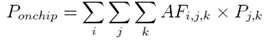 Note that AFi;j;k is 0 if data section i is either not mapped to logical memory bank j, or if i not mapped to physical memory bank k. Also, AFi;j;k and AFi;j;k` would both account for an access to data section i that is mapped to logical memory bank j, when j is implemented using multiple banks k and k`. For example, logical memory bank of 2KX 16 implemented using two physical memory modules of size 2K X8. Thus the total power Mpow for all the memory banks including off-chip memory is given by
  where AFi;off represents the number of access to off-chip memory from data section i, and Poff is power per access for off-chip memory. Once the memory cost and memory cycles are computed for all the individuals in the population, individuals are ranked according to the optimality conditions on power consumption (Mpow) and performance in terms of memory stall cycles (Mcyc). More speci¯cally, if (Ma pow;Ma cyc) and (Mb pow;Mb cyc) are the memory power and memory cycles of chromosome A and chromosome B, A is ranked higher (i.e.,has a lower rank value) than B if
  The ranking process in a multi-objective GA proceeds in the non-dominated sorting manner. All non-dominated individuals in the current population have a rank value 1 and are flagged. Subsequently rank-2 individuals are identified as the non-dominated solutions in the remaining population. In this way all chromosomes in the population get a rank value. Higher fitness values are assigned for rank-1 individuals as compared to rank-2 and so on. This fitness is used for the selection probability. The individuals with higher fitness gets a better chance of getting selected for reproduction. To ensure solution diversity which is very critical for getting a good distribution of solutions in the optimal front, the fitness value is reduced for a chromosome that has many neighboring solutions.
4. Implementation
- For our experiments, the main inputs are the access characteristics of the data sections. We need the sizes of the data sections, access frequency of each of the data sections and the conflict matrix. The access frequency and the conflict matrix are obtained from a software profiler. Since the DSP applications typically have simple control flow, the profile information on the access characteristics does not change very much from run to run.
|
|
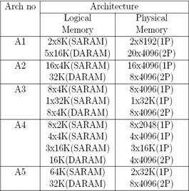
5. Results
- The Voice Encoder application for the 5 different architectures A1-A5.
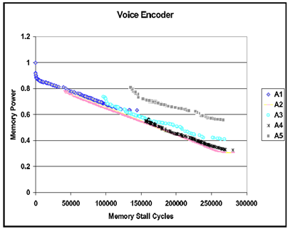 The solution points of A1 are clearly superior here, mainly in terms of performance. Observe that the solution points of the architectures A1, A2 and A4 dominate some of the power-performance regions in the data layout space. Solutions of A1 dominate the high performance space, solutions of A2 and A4 dominate the middle space both in performance and power, and again solutions of A2 dominates the low power-performance region. From the results, it can be deduced that for voice encoder, DARAM and multiple memory banks both are equally critical. With only a small increase in area compared to A5, A3 achieves much better performance than A5. This is due to the higher number of banks in A3 that resolves more parallel conflicts. Typically, hand optimized assembly code will try to exploit the DSP architectures by using multiple simultaneous accesses and self accesses.
 6. Conclusions
- In this chapter we presented a Data placement approach for physical memory architecture. We demonstrated that there is significant trade-off up to 60% between power and performance. For a given memory architecture, the placement of data sections is crucial to the performance of the system. Badly placed data can result in a large number of memory stalls. We consider a memory architecture that consists of on- chip single-access RAM with multiple memory banks, on chip Dual-access RAM, and external RAM. We analyze the application for data conflicts and create a matrix representation of the conflict information. The Genetic algorithm is utilized for the performance and power minimization.