A. Bakhtiari, T. Berberashvili, P. Kervalishvili
Engineering Physics faculty, Georgian Technical University, Tbilisi, Georgia
Correspondence to: A. Bakhtiari, Engineering Physics faculty, Georgian Technical University, Tbilisi, Georgia.
| Email: |  |
Copyright © 2022 The Author(s). Published by Scientific & Academic Publishing.
This work is licensed under the Creative Commons Attribution International License (CC BY).
http://creativecommons.org/licenses/by/4.0/

Abstract
Today Graphene with its unusual properties is one of the most interesting materials useful in different applications. Graphene’s sensitive properties are highly correlated with its macro and nanostructure, hence the preparation process of Graphene structures is very significant. During the last decades, several methods of producing Graphene-like structures and their thin films onto a substrate were developed and each of them has some advantages. At the same, it is still problematic to receive thin nanostructures with suitable lattice quality and uniformity. In this regard, the flexibility and accuracy of a method play the main role. In this work, the Graphene thin film preparation process based on a precise, accurate, and feasible method as Continuous Wavelength Laser Deposition (CWLD) was introduced. However, this article focused on Graphene thin film, but CWLD can be used for different materials.
Keywords:
Continuous wavelength laser, Thin film, Graphene, Graphite exfoliation, Deposition
Cite this paper: A. Bakhtiari, T. Berberashvili, P. Kervalishvili, Preparation of Graphene Structures by Continous Wavelength Laser Deposition Method, American Journal of Condensed Matter Physics, Vol. 12 No. 1, 2022, pp. 1-5. doi: 10.5923/j.ajcmp.20221201.01.
1. Introduction
Generally, Carbon has 3 known allotropic crystalline structures diamond, graphite, and coal. In the recent years, new structural modification of graphite, and graphene is discovered [1,2]. The main difference between the Carbon structures is bonding strength in different directions. Diamond has the strongest bonding in 3 directions. Graphite has 2 strong bonding and a weaker one in the z-direction [3].Graphene is an allotrope of carbon consisting of a single layer of atoms arranged in a two-dimensional honeycomb lattice. Each atom in a graphene sheet is connected to its three nearest neighbors by a σ-bond and contributes one electron to a conduction band that extends over the whole sheet. These conduction bands make graphene a semimetal with unusual electronic properties that are the best described by theories for massless relativistic particles [3]. 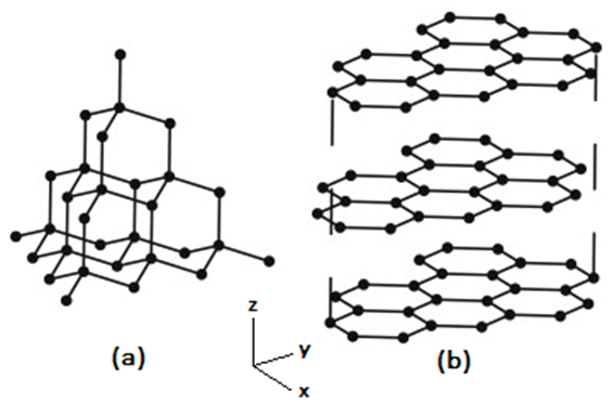 | Figure 1. (a) Diamond structure, (b) Graphite structure |
Charge carriers in graphene shows linear, and charge transport is ballistic over long distances. Graphene conducts heat and electricity very efficiently along its plane. The material strongly absorbs light of all visible wavelengths and a single graphene sheet is nearly transparent because of its extreme thinness. The material is also about 100 times stronger than would be the strongest steel of the same thickness.The stacked parallel layers in bulk graphite are separated by 0.34 nm. Although the van der Waals attraction between the layers is weak enough to let them slide past each other in the direction perpendicular to the z-axis, the attraction is strong enough to make complete exfoliation into individual layers (Graphene) difficult. The first attempt by Brodie to produce single-layer graphene sheets by exfoliation dates as far back as 1859. Graphite oxides synthesized by one and two-step Brodie oxidation (BGO) and Hummers (HGO) methods were analyzed by a variety of characterization methods to evaluate the reasons behind the difference in their properties. It is found that the Brodie method results in a higher relative amount of hydroxyl groups and a more homogeneous overall distribution of functional groups over the planar surface of the graphene oxide flakes [4]. Since then, many attempts have been made at the large-scale production of graphene with little success. It has likely been unknowingly produced in small quantities for centuries, through the use of pencils and other similar applications of graphite. It was originally observed in electron microscopes in 1962 but only studied while supported on metal surfaces. The material was later rediscovered isolated and characterized in 2004 [5]. Later prompted new efforts to produce two-dimensional materials by exfoliation were introduced. It was underlined that for successful exfoliation, overcoming the van der Waals attractions between the adjacent layers is necessary [6].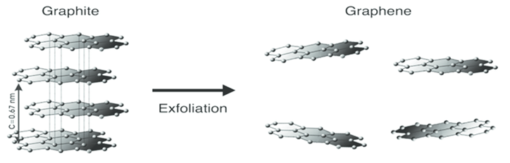 | Figure 2. Graphite exfoliation provides Graphene |
Three of the four outer-shell electrons of each atom in a graphene sheet occupy three sp2 hybrid orbitals that are shared with the three nearest atoms, forming σ-bonds. The length of these bonds is about 0.142 nanometres same as graphite [1]. The remaining outer-shell electron occupies a pz orbital that is oriented perpendicularly to the plane. These orbitals hybridize together to form two half-filled bands of free-moving electrons, π and π, which are responsible for most of graphene's notable electronic properties [7].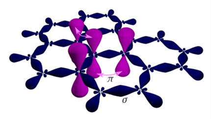 | Figure 3. Graphene structure |
Graphene’s high electrical and thermal conductivity and Graphene transparency depend on its lattice quality and layers thickness [8].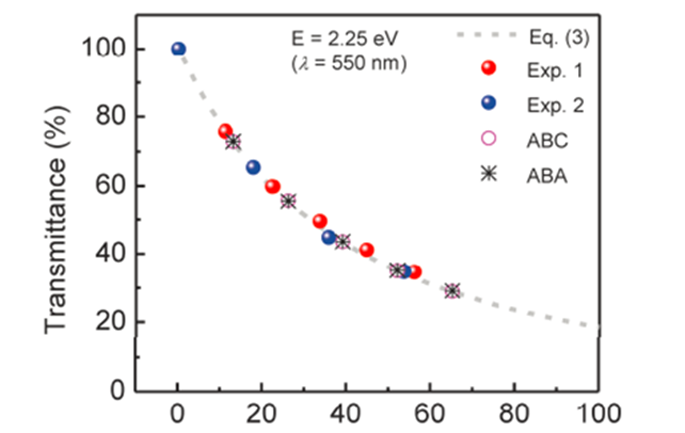 | Figure 4. Number of Graphene layer correlated to its Transparency [8] |
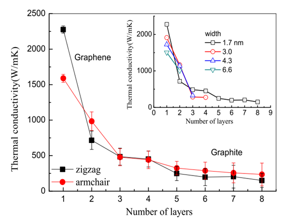 | Figure 5. Thermal conductivity and thickness correlation [8] |
2. Exfoliation Methods
Generally, there are 3 different types of exfoliation methods.1. Mechanical 2. Physical Vapor Deposition (PVD)3. Chemical Vapor Deposition (CVD)Mechanical is based on the Geim - Novoselov method. Graphene layer from Graphite should be stucked out with an adhesive tape such as scotch and pasted onto the substrate. Physical and chemical vapor deposition are based on substrate immersion in the vapor. Then, the substrate is become a larger mass due to material transference from vapor onto the solid. If the vapor is created only by a physical, the process is called physical vapor deposition (PVD) and if the vapor is created by a chemical reaction, the process is classified as chemical vapor deposition (CVD). Anyway, the deposition is carried out in a vacuum chamber to enable control of the vapor composition in a clean volume. Meanwhile, in the PVD, the material transmission from the target onto the substrate could be evaporating, or sputtering. In the evaporating process, thermal energy is supplied to the target from which atoms are evaporated for deposition onto the substrate. The vapor source configuration is intended to concentrate heat on the target material. Heating can be accomplished by any of several methods (laser, resistance heating wire, high-frequency induction, electron beam, etc.) [8].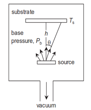 | Figure 6. General PVD or CVD thin film technology |
In sputter deposition, ions of a sputtering gas, are accelerated toward the target at high speed by an imposed electric field. The initial concentration of charge carriers in the system is significantly increased with an increase in the dc voltage, as the ions collide with the cathode, thereby releasing secondary electrons, and with the neutral gas atoms [9].The methods investigating show mechanical exfoliation consumes low energy, but it could not be used for thin and brittle substrates such as photovoltaic solar cells. Also, thin-film lattice uniformity on the substrate could be considered a mechanical exfoliation deficiency. In this regard, CVD and PVD can be the suitable method, but from an energy consumption point of view, they are not good as mechanical exfoliation. Graphene thin-film properties depend on its crystal structure quality and uniformity. There are two types of thin-film structures microstructural and atomical and high-quality structure comes out of atomical structure considerations. However, sputtering and evaporating can provide atomical structure, but surface diffusivity via sputtering (because of high energic atoms bombardment) and non-epitaxial growth of the thin film on the substrate surface represent that in this case sputtering cannot be a high-quality method. Therefore, evaporation is the best process. Also, the evaporation method essence is heating. In other words, the key operator to control the thin film is thermal energy. In the late eighties of the last century, the laser plasma method of preparation of Carbon-based materials was introduced. Dimond-like, Boron and different metal Carbide films were prepared and investigated [10]. Hence, in this work, based on the laser plasma concept a novel exfoliation method as Continuous Wavelength Laser Deposition (CWLD) is introduced. It is very important that for our method not only its low energy consumption is significant, but also the best quality of thin-film structure which is achievable by the usage of different accurate and precise operators.The investigating methods show that mechanical exfoliation consumes low energy, but it could not be used for thin and brittle substrates such as photovoltaic solar cells. Also, thin-film lattice uniformity on the substrate could be considered a mechanical exfoliation deficiency. In this regard, CVD and PVD can be in general the suitable method, but from an energy consumption point of view, they are not good as mechanical exfoliation.
3. CWLD Exfoliation Method
In this method, the target is evaporated by a laser beam and deposited onto the substrate surface. In this process, the target and substrate are 90° angular distance, and a CW laser is the source of energy. Ions of plasma plume deposit on the substrate gravitationally [11].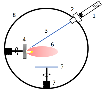 | Figure 7. Schematic illustration of CWLD. (1) Laser source, (2) Laser window, (3) Laser beam, (4) Target, (5) Substrate, (6) Plume’s ions, (7) Rotor, (8) Vacuum chamber [11] |
Ions' gravitational falling gradient provides uniform deposition onto the substrate. Hence, ions conjunction horizontally and vertically is expected. In other words, not only Graphene lattice will be high quality, but also the thin-film thickness will be uniform everywhere on the substrate. CWLD was modeled mathematically by the Dynamic Fractal doctrine to find the best thin-film quality [12]. There are different operators such as target-substrate distance, laser beam diameter, laser wavelength, laser-target radiation angle, target material grain size, vacuum level, and laser power that make the process an accurate and flexible system. Therefore, the thin film could be adjusted by the application exactly. Also, its low energy consumption makes it a cheap method for industrial production. The most similar laser evaporating to CWLD is Pulsed Laser Deposition (PLD). The target is evaporated by a laser beam and deposited onto the substrate surface. In this process, the target and substrate are parallel, and a pulsed laser is the heat source. However, PLD is categorized as an evaporating method, but ions through plasma are sputtered onto the silicon. Then, PLD is semi-same as sputtering. This method has been used extensively to manufacture thin films of various materials such as oxides, nitrides, carbides, organic materials, and metals [13].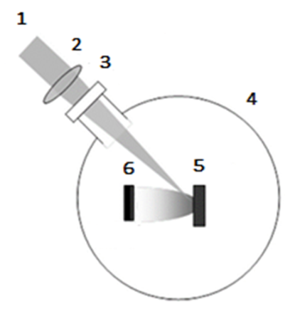 | Figure 8. Schematic illustration of PLD. (1) Pulsed laser beam, (2) Focus lens, (3) Laser window, (4) Vacuum chamber, (5) Target, (6) Substrate. [14] |
4. Test Results
A case study shows the CWLD method’s advantages. Using n-type silicon as substrate, a laser beam with 3 mm diameter, 450 nm wavelength, and 10 watts nominal power was used the graphene layers were deposited. The laser source was located at 40 cm from the target at 23° angle. Also, a piece of heat graphite was utilized as a target and was radiated for 1 hour by the laser source. In performing experiments, the level of vacuum level was about 10-3 Torr, which determined the existence of pure Graphene plus Graphene oxide. This was shown in Figure 9. 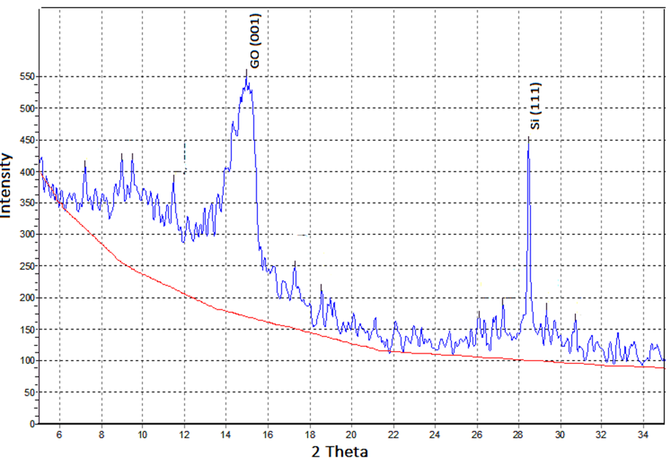 | Figure 9. XRD test result of CWLD method |
The performance of the CWLD would be more clear in comparison to mechanical exfoliation by scotch tape (Figure 10). 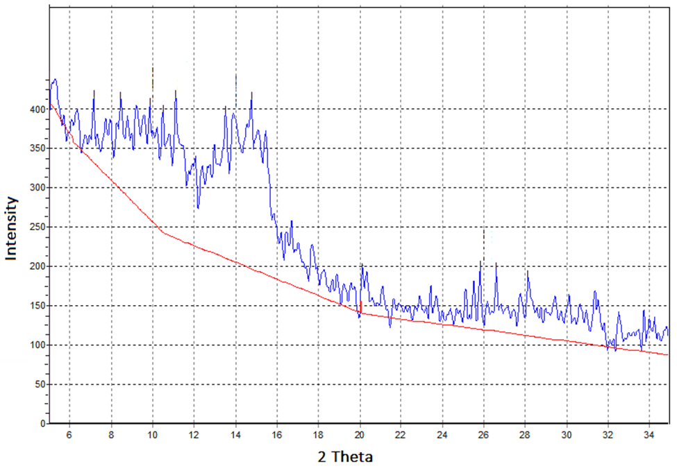 | Figure 10. XRD of mechanical exfoliation with scotch tape |
In the graph (figure 9), 2θ is 15°, FWHM is 0.0139626 radian, and d is 5.90 Å. Results comparison to an ideal Graphene structure (Figure 11) clears the CWLD capability. 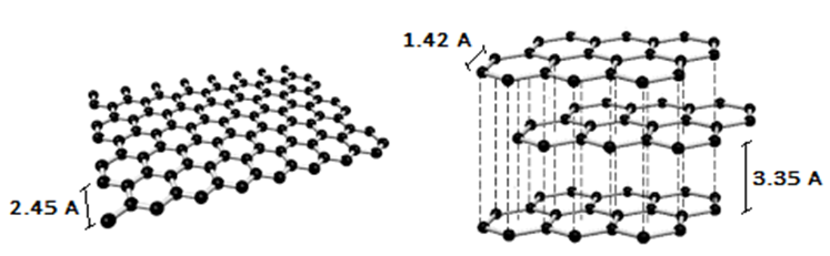 | Figure 11. Ideal Graphene layer structure |
5. Conclusions
According to the flexibility of CWLD, any operator (such as laser power, target-substrate distance, target-laser beam angle and so on) changes provide a new structure that shows the capability of the method. At the same time this work related to preparation of different Graphene structures as layers, and nanostructured films, has shown the flexibility and accuracy of the method that gives a possibility of preparation of any structure of any material with the necessary thickness. Today 2D materials are utilized in many industries and one of the significant parameters to find a feasible final product is energy consumption. Low energy consumption of the CWLD is another important achievement that makes it an effective method for thin film industrial production.
ACKNOWLEDGEMENTS
We are thankful to all of Micro & Nanoelectronics institute (IMNE) members who provided expertise that greatly assisted us for samples preparation and testing.
References
| [1] | Hoffmann, R.; Kabanov, A.; Golov, A.; Proserpio, D. (2016). "Homo citans and carbon allotropes: For an ethics of citation". Angewandte Chemie. 55 (37): 10962–10976. doi:10.1002/anie.201600655. |
| [2] | Meyer, J.; Geim, A. K.; Katsnelson, M. I.; Novoselov, K. S.; Booth, T. J.; Roth, S. (2007). "The structure of suspended graphene sheets". Nature. 446 (7131): 60–63. arXiv: cond-mat/0701379. Bibcode: 2007 Natur. 446...60M. doi:10.1038/nature05545. |
| [3] | G. Abdushelishvili, A. Bakhtadze, P. Kervalishvili, G. Tkeshelashvili. Laser deposition of a substance from the gas phase and mass transfer in the beam field. J. Physics and Chemistry of Materials Processing, No.-3, 1987. USSR. |
| [4] | Alexandr V Talyzin, Guillaume Mercier, Alexey G. Klechikov Alexey G. Klechikov, et all. Brodie vs graphite oxides for preparation of multi-layered materials, January 2017, Carbon 115 DOI: 10.1016/j.carbon.2016.12.097. |
| [5] | Geim, A. K.; Novoselov, K. S. "The rise of graphene". Nature Materials, 6 (3): 183–191, 2007. |
| [6] | Ahmed A. MOOSA, and Mayyadah S. ABED. Graphene preparation and graphite exfoliation. Turk J Chem. 2021; 45(3): 493–519, Published online 2021 Jun 30. doi: 10.3906/kim-2101-19. |
| [7] | Heyrovska, Raji, "Atomic Structures of Graphene, Benzene and Methane with Bond Lengths as Sums of the Single, Double and Resonance Bond Radii of Carbon", 2008. |
| [8] | L. B. Freund, S. Suresh. Brown university - MIT, Thin film materials, USA, 2003. |
| [9] | Sproul, W. D.; Christie, D. J.; Carter, D. C. (2005-11-22). "Control of reactive sputtering processes". Thin Solid Films. 491 (1): 1–17. doi:10.1016/j.tsf.2005.05.022. ISSN 0040-6090. |
| [10] | P. Kervalishvili Shalamberidze S. Esadze G. Porta P. Semiconductor material film production by laser plasma deposition. Le Vide, le Couches minces, N-167, 1993, pp. 189-198. |
| [11] | Tamar Berberashvili, Lali Chakhvashvili, Habibollah Bakhtiari, Gela Goderdzishvili, Paata Kervalishvili. Silicon–graphene based solar elements. Book of abstract 6th International Conference “Nanotechnology”, Georgian Technical University, 4 – 7 October 2021, Tbilisi, Georgia, p.14. |
| [12] | A. Bakhtiari, P. Kervalishvili, Dynamic Fractal Doctrine as Nonlinear Systems Model, American Journal of Condensed Matter Physics 2021, 11(1): 1-6, DOI: 10.5923/j.ajcmp.20211101.01. |
| [13] | Paata J. Kervalishvili, Laser technologies of nanosystems preparation. Conference “Nanotechnology”, Georgian Technical University, 4 – 7 October 2021, Tbilisi, Georgia, p. 62. |
| [14] | Hiroshi Fujioka, Handbook of crystal growth, Institute of industrial science, University of Tokyo, Elsevier, 2015. |

 Abstract
 Reference
 Full-Text PDF
 Full-text HTML