-
Paper Information
- Paper Submission
-
Journal Information
- About This Journal
- Editorial Board
- Current Issue
- Archive
- Author Guidelines
- Contact Us
American Journal of Condensed Matter Physics
p-ISSN: 2163-1115 e-ISSN: 2163-1123
2017; 7(2): 41-49
doi:10.5923/j.ajcmp.20170702.02

Electrical Conduction and Dielectric Relaxation in Selenium Films Doped with Dysprosium Rare Earth
 Abstract
 Reference
 Full-Text PDF
 Full-text HTML
Fathy A. Abdel-Wahab, Heba Abdel Maksoud
Physics Department, Faculty of Science, Ain Shams University, Abbassia, Cairo, Egypt
Correspondence to: Fathy A. Abdel-Wahab, Physics Department, Faculty of Science, Ain Shams University, Abbassia, Cairo, Egypt.
| Email: |  |
Copyright © 2017 Scientific & Academic Publishing. All Rights Reserved.
This work is licensed under the Creative Commons Attribution International License (CC BY).
http://creativecommons.org/licenses/by/4.0/

Selenium (Se) films implanted with Dysprosium (Dy) atoms are prepared using thermal evaporation technique. The temperature dependence of ac conductivity measured in frequency range 50 Hz-80 KHz is found to be proportional to ωs  This proportionality is reasonably well interpreted, in the low temperature region, by correlated barrier hopping (CBH), of bi-polaron between both random and paired defect states. In the same time the high temperature part the ac conductivity is well fitted using Mayer-Neldel rule. Furthermore, the dielectric relaxation times of the doped a-Se films are determined from the dependence of the loss factor
  on the applied frequency relations. The Cole-Cole diagrams have been presented and are used to determine the values of the static
  and optical
  dielectric constants of a-Se doped with Dy atoms.
Keywords: Amorphous Selenium, Doped chalcogenides, Rare earths, ac conductivity, Dielectric relaxation and loss, Cole-Cole diagram
Cite this paper: Fathy A. Abdel-Wahab, Heba Abdel Maksoud, Electrical Conduction and Dielectric Relaxation in Selenium Films Doped with Dysprosium Rare Earth, American Journal of Condensed Matter Physics, Vol. 7 No. 2, 2017, pp. 41-49. doi: 10.5923/j.ajcmp.20170702.02.
Article Outline
1. Introduction
- Rare-earth (RE)-doped glass fiber amplifiers operating at a 1.3 μm wavelength band have received extensive attention due to the zero dispersion of the silica fiber glass in the 1.3 μm-wavelength region, and most installed fibers worldwide are optimized at this wavelength. [1-4]. In contrast, Dysprosium rare earth atoms, Dy which have an active unfilled f shells in its electronic configuration ([Xe] 4f104s2), can provide 1.3 μm emission due to the 6F11/2, 6H9/2→6H15/2 transition [5]. In addition, Dy has a good absorption band at approximately 800 nm, at which level a cheap commercial laser diode could be used for excitation. On the other hand, amorphous Selenium (a-Se) is characterized by existence of localized states in its mobility gap. These states are created due to presence of defects and absence of long range order [6-8]. The structural disorder made a-Se and its alloys to have a high optical transparency in the infra-red (IR) spectral regions up to 10 μm. Besides, it has large refractive index, thermal stability and high degree of covalent bonding. Furthermore, due to high rare earth solubility, high emission quantum efficiency [9] and the low phonon energy (~ 250 cm-1) of amorphous selenides compared with fluorides (~ 550 cm-1), or oxide glasses (~ 1100 cm-1) [10] it could be used as a host medium for Dy to enhance its mid-IR laser emission. It should be noted that the low phonon energy of a-se decreases the multi phonon relaxation which enables an active transitions between rare earth atom levels in the middle IR spectral region. The optical excitation and emission of Dy is very sensitive to the surrounding media considerations such as dielectric parameters which plays an important role to control the relaxation processes and consequently the performance of the laser emission of Dy [11].In the present work, the dependence of ac conductivity on the applied frequency and temperature are analyzed with reference to the current conduction models. The analysis showed that the correlated barrier hopping over barriers (CBH) is the most probable model to describe the a.c. conduction mechanism in the low temperature range. Furthermore, the modified CBH with Mayer-Neldel rule is well fitted with the ac conduction in the high temperature range. The dependence of the loss factor (ε") on the applied frequency and Cole-Cole diagrams showed that the dielectric relaxation times for Se-Se and Se-Dy dipoles are 2.46x10⁻⁵ and 1.27x10⁻⁴ s in sequence.
2. Experimental
- Bulk Selenium sample of weight 3g and doped with 0.008 (at. %) of dysprosium (Dy) is prepared by mixing appropriate quantities of Se and Dy, of purity 5N, in evacuated pre-cleaned silica tube sealed at 10-5 Torr. The synthesis of the mixture was carried out by heating the ampoule in an electric furnace to 400°C and keeping it at this temperature for 3 hrs. Then, the temperature (T) was gradually raised by a rate of ~ 200°C/h to 900°C and kept again at that temperature for another 9 hrs. Finally, the ampoule is left to cool down to room temperature (RT=25°C). The obtained bulk ingots were used as source materials to prepare thin film samples by the thermal evaporation technique using vacuum coating unit type Edwards E306 A. The base pressure of the vacuum system was 1.5x10⁻⁶ Torr. After evaporation, the thickness of the fresh films was accurately determined by an optical interference method and is found to be 750 nm. The structure of the obtained films are studied using x-ray diffraction computerized system (model: Philips EXPERT-MPDUG PW-3040 diffractometer with Cu Kα radiation source) in the 2θ range 0–90°. For electrical characterization, sandwich structure devices consisting of Au/Se:Dy/Au were prepared in situ by thermal sublimation under high vacuum (~10-5 Torr). A programmable voltage–current source (type Keithley 228 A) was used as a source of applied voltage and a Keithley-616 digital electrometer was used to measure the output current. The electrical conductivity measurements were done under vacuum and steady state conditions, using lock-in amplifier model Oxford-DN 1714 in the temperature range 312-82 K and frequency range 50 Hz–80 kHz in the dark conditions.
3. Results and Discussion
- The recorded XRD patterns for the studied as-prepared a-Se, previous work of SeSm0.008 films [12] and Dy doped Se (present work) samples are shown in figure (1). In this figure, the XRD pattern of the fresh Se films reflects its amorphous nature. Furthermore, the doped Se film with 0.008 at.% Sm [12] reflects an amorphous matrix embedded with some crystalline zones. These zones appear throughout two characteristic selenium lines lying in the region of the main diffraction hump covering roughly the range of 23-32 in 2θ° angular units. Disappearance of such diffraction hump in case of Se doped with 0.008 at. % Dy (present work) mean the growth of crystalline phase on the expense of amorphous state. This crystalline phase consists of mixed phases of elemental Se (100), (101), (012), (110), (111), (022) elemental Dy (102), (110) and SeDy with tetragonal (002), (003), (112) and orthorhombic (603), (116), (117) structures as shown in Fig. (1).
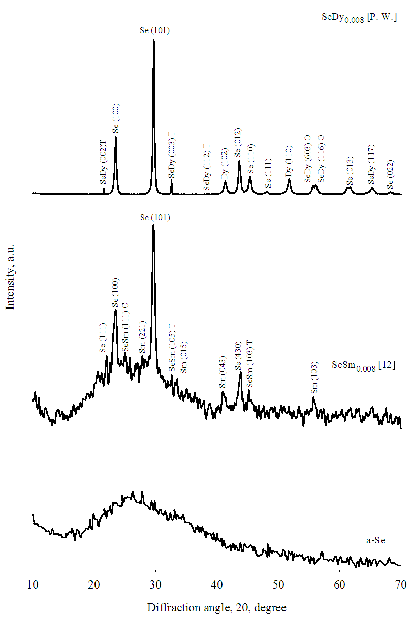 | Figure (1). XRD pattern for a-Se, previous work of SeSm0.008 [12] and the present work [P. W.] of SeDy0.008 thin films. It should be noted that the diffraction pattern of SeSm0.008 [12] is added to the figure for the sake of comparison |
3.1. Electrical Conduction
3.1.1. ac Conduction
- The temperature dependence of ac conductivity (σac) of the investigated samples at different values of frequency is shown in Fig. (2). For clarification purpose, not all the recorded frequency data points are represented in the figure. In this figure, the ac conductivity shows a frequency dependence which becomes more pronounced at higher frequencies. On the other hand, and in low temperature range (82-152 K) the conductivity increase slightly less than linear against temperature and tends to become a temperature dependent at higher temperatures (152-312 K) in the studied frequency range. The graphical relation between the applied frequency and ac conductivity (σac) at different temperatures is shown in Fig. (3). This figure illustrates that σac depends on temperature nearly in the whole studied frequency range. The enhance of ac conductivity at any frequency and temperature may be explained as follows: the Dy atoms enters the structural network of a-Se with coordination number of 7-8 bonds to Se with bond length from 2.92 to 2.97 °A [13]. This means that a redistribution of electronic charges takes place which built up a space charge region around Dy atom and the surrounding Se atoms resulting an increase in σac.
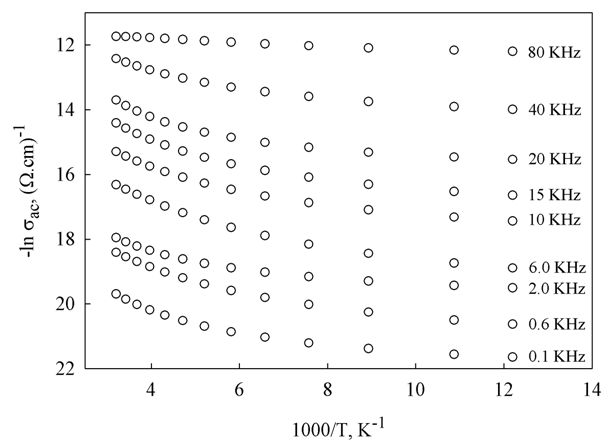 | Figure (2). Temperature dependence of ac conductivity for SeDy0.008 thin films measured at different frequencies |
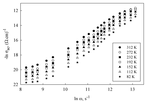 | Figure (3). ac conductivity dependence on frequency for the studied SeDy0.008 thin films measured at different temperatures |
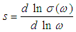 which is used to determine the a.c. conduction mechanism [15]. The temperature dependence of the exponent s calculated using Fig. (3) is shown in Fig. (4). This figure illustrates that the highest value of s is obtained at a lower measured temperature and decreases gradually with increasing temperature to reach a minimum value at T = 312 K.
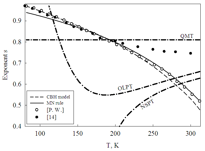 | Figure (4). Temperature dependence of the frequency exponent s (open circles) for the studied thin film samples [P. W.] obtained from slopes of Fig. (3). The dash-dotted curves represent the values calculated using the models: QMT [14], NSPT [14], OLPT [17] while the solid line represents the MN rule (Eq. (6)). The dashed curve represents the CBH model (Eq. (1)). The values of s calculated for Bismuth-Vanadate glassy semiconductor [14] are inserted in the figure for the sake of comparison |
 | (1) |
 | (2) |
 | (3) |
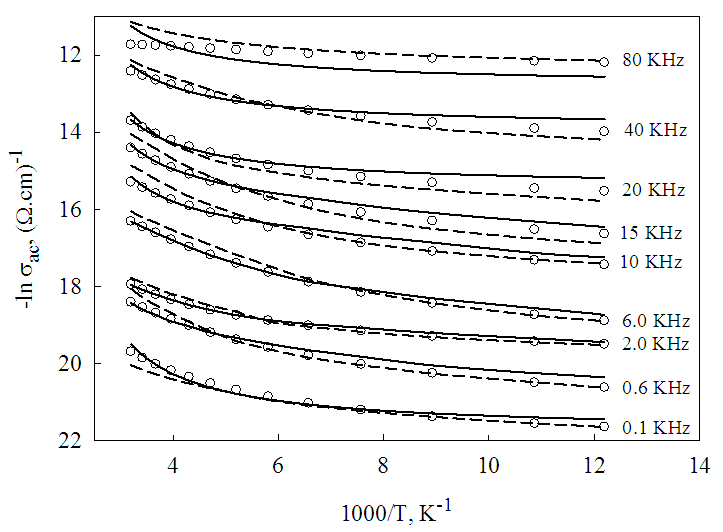 | Figure (5). Temperature dependence of ac conductivities measured at different frequencies for the studied thin films. The open circle symbols correspond to experimental data. The dashed curves represent the fitting of ac conductivity using the CBH model (Eq. (2)) while the solid curves are the fitting using the MN rule (Eq. (5)) |
3.1.2. Modification of CBH Model using MN Rule
- It is known that the CBH model explains the variation of σac(ω) with temperature at relatively low temperature and does not predict the strong temperature dependence at high temperatures [21, 22]. Mayer-Neldel (MN) [23] has improved the CBH model in order to account for the ac conductivity, σac, and for the frequency exponent s in the high temperature range. In the case of thermally activated processes, the MN rule states that the electric conductivity can be expressed by Arrhenius relation
 the dependence of the pre-exponential factor,
  and activation energy,
  in its logarithmic form is given by:
 | (4) |
 and
and  are constants and refer to the normal and inverted MN rule in sequence. To apply MN rule on the studied samples, obtain the slopes and pre-exponential factors of the curves in Fig. (2) in the high temperature region. Plot the graphical representation of the pre-exponential factor,
  and activation energy, , is shown in Fig. (6). The data points shown in Fig. (6) obey Eq. (4). Also, in this figure, it is observed that the experimental data at low frequencies obey the normal MN rule, while the high frequency data are found to obey the inverted MN rule. Obtained values of
  and
and  for the studied samples are 5.7x10⁻⁸ (Ω.cm)-1, 6x10⁻⁶ (Ω.cm)-1, 845 K and 580 K respectively.
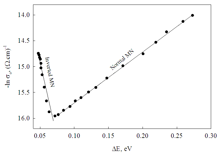 | Figure (6). Normal and inverted Meyer–Neldel plots for the studied samples. The symbols represent the experimental data and the straight lines are the best fit to the experimental data using least squares fits |
 | (5) |
 While the power exponent s obeys the following relation:
 | (6) |
 term
term  which differentiate between the conductivity of CBH model (eq. (2)) and MN rule (eq. (5)) has a big role in the conductivity of the system. As temperature increase,
  decrease which increase the conductivity term in MN rule over the CBH model. On the other hand, at low temperature the value of ζ increase leading to a decrease of the conductivity value of CBH model over the MN rule.
 3.2. Dielectric Properties
- Figure (7) shows the dependence of both real, ε', and imaginary, ε" parts of the complex dielectric constant on the applied angular frequency for the investigated samples in the studied temperature range. In this figure the real part of the dielectric constant, ε', changes only slowly with frequency in the low frequency range (400 Hz - 3.0 kHz) and decreases more rapidly at higher frequencies (3.0 - 80 kHz). Furthermore, in this figure it is observed that loss factor ε" exhibits two relaxation peaks in the low and high frequency regions. Appearance of these two peaks could be explained as follows: According to oscillator model of Lorentz [26] the natural resonant frequency of dipole is determined by
 where μ is the reduced mass of the two oscillators of the dipole and ks is the restoring force of the spring that connects them. It is known that doping of Selenium with Dy ions creates a Se-Dy bonds besides the Se-Se bonds of a-Se. Taking into consideration the atomic masses of Se (78.96) and Dy (162.5) we can conclude that for Se-Dy bonds, ωo will shift towards lower frequencies with respect to the Se-Se bonds and causes the formation of the peak at lower frequency as shown in Fig. (7). According to this model, the transition time τ of the two peaks (τ1 and τ2) could be calculated as the reciprocal of the angular frequency at the top of the loss peak. The calculated average values of τ1 and τ2 for the investigated samples calculated from ε"=f(ω) are 1.72x10⁻⁴ s and 2.31x10⁻⁵ s respectively.
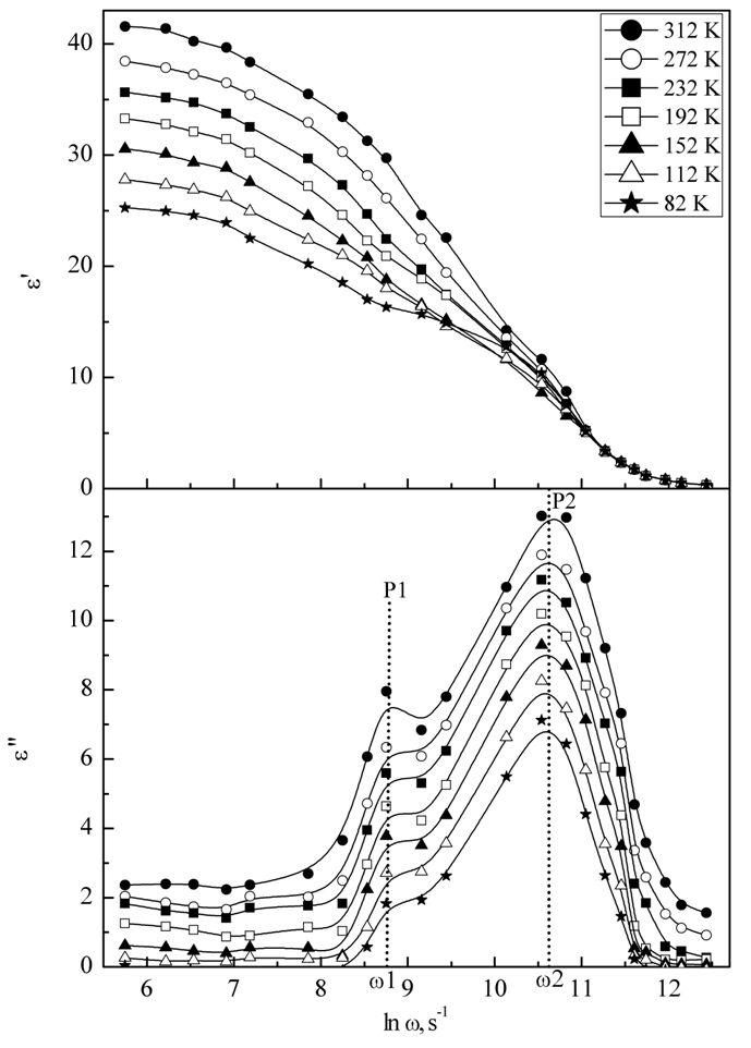 | Figure (7). Dependence of the real, ε', and imaginary, ε" parts of the complex dielectric constant on the applied angular frequency for the investigated samples in the studied temperature range |
 at higher frequencies. The difference between values of εs and
  is attributed to the polarization of the oscillating dipole [27]. In this case, the relation between εs,
  and ε* is given by Cole and Cole [28] as:
 | (7) |
 | (8) |
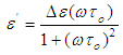
 The dependence of ε" on ε' is obtained by applying the Cole–Cole model for the investigated samples in the studied temperature range and is shown in Fig. (8). In this figure, the symbols represents calculated data with the solid line showing the best fit to the calculated data using Eq. (7). After extrapolating the fitted values to the real axis (ε'-axis), the plot shows that, for lower frequency the experimental points deviate from the dashed semicircles giving different values of the dielectric constant εs in the studied temperature range as shown in the inset of Fig. (8). In this inset of the figure it is clear that, in the low temperature region up to 200 K static dielectric constant, εs, changes by ratio ~ 26% against temperature while at higher temperatures (T > 200 K) the dependence becomes more pronounced and εs increase by 58%. The direct proportion between εs and temperature is due to the dependence of the static dielectric constant on the lattice oscillations of the host material [25]. On the other hand in Fig. (8), at higher frequencies, all the data at different temperatures converge in one point that represents a unique value of optical dielectric constant,
  The calculated values of
  for samples under study are 1.82. It should be noted that presence of two dielectric constants εs and
  suggest the presence of two relaxation processes with time constants whose values are rather close to each other.
  | Figure (8). Cole–Cole diagram for the investigated thin film samples at different temperatures. The solid curves drawn are the fitting of Cole–Cole equations to the calculated values of ε' and ε". The dependence of the calculated εs on the applied temperature are represented in the inset |
4. Conclusions
- A comprehensive electric and dielectric study on the effect of doping of a-Se thin films with 0.008 at. wt.% of Dy in the temperature range 312–82 K and frequency range 50 Hz–80 kHz allows us to draw the following conclusions:(1) A graphical relation between ac conductivity and temperature illustrated a strong temperature dependence and small frequency dependence (f ≤ 40 kHz) for σac in the region of high temperature (312 K ≥ T >152 K). While for f > 40 kHz, σac depends mainly on the applied frequency and this dependence decreases as frequency increases.(2) The calculated values of the power exponent s showed decreases from high to low values with increasing temperature.(3) Among the different calculated ac conduction models, the CBH model is fitted fairly well with the experimental data of the function σac = f(T) in the low temperature range (82-187 K) with a deviation in the high temperature range.(4) The calculated values of normal and inverted MN parameters (
 and
and  ) are used to fit the measured electrical conductivities of investigated film samples. A reasonable fitting appears in the high temperature region (187-312 K) with a deviation in the low temperature range. (5) The arc shape of the Cole–Cole diagram leads to one value for the optical dielectric constant,
  and different values for the static dielectric constant εs, throughout the temperature range, 312–82 K.