-
Paper Information
- Paper Submission
-
Journal Information
- About This Journal
- Editorial Board
- Current Issue
- Archive
- Author Guidelines
- Contact Us
American Journal of Condensed Matter Physics
p-ISSN: 2163-1115 e-ISSN: 2163-1123
2017; 7(1): 6-16
doi:10.5923/j.ajcmp.20170701.02

AC Impedance Response and Electrical Conduction Mechanism of Thin Selenium Films Doped with Samarium Atoms
 Abstract
 Reference
 Full-Text PDF
 Full-text HTML
Fathy A. Abdel-Wahab, Heba Abdel Maksoud
Physics Department, Faculty of Science, Ain Shams University, Cairo, Egypt
Correspondence to: Fathy A. Abdel-Wahab, Physics Department, Faculty of Science, Ain Shams University, Cairo, Egypt.
| Email: |  |
Copyright © 2017 Scientific & Academic Publishing. All Rights Reserved.
This work is licensed under the Creative Commons Attribution International License (CC BY).
http://creativecommons.org/licenses/by/4.0/

The dielectric parameters of Sm doped Se films (namely SeSm0.008) films prepared by thermal evaporation were measured under vacuum in a wide range of frequency and temperature. The measured real part of the admittance (Y') versus frequency (f) were analyzed and shows two distinct regions. In the first one which lie in the low frequency range Y' displayed an independence on the frequency that give a direct evidence for the existence of Debye model. In the high frequency part, which is considered using power low:  (n ≤ 1.0), a deviation from Debye model is observed where Y' increase linearly against frequency. Analysis of the calculated values of n with reference to those numerically calculated for different theoretical a.c. conduction models shows that correlated barrier hopping (CBH) is a fairly good to describe the dominant conduction mechanism. The equivalent circuit approach is applied by comparing the theoretical and experimental data trends of the plots of Z'-Z and Y'-Y as function of frequency for all proposed equivalent circuits and showed that R║C connected in series with R║C║CPE is the most appropriate circuit to represent the structure of the investigated films. Furthermore, the dc conductivity calculated using the obtained values of the resistances, R, versus temperature are plotted and discussed according to the current dc conduction theories.
Keywords: Se doped Sm, Se doped rare earth, Thin films, Equivalent circuit approach, Impedance spectroscopy, Electrical admittance
Cite this paper: Fathy A. Abdel-Wahab, Heba Abdel Maksoud, AC Impedance Response and Electrical Conduction Mechanism of Thin Selenium Films Doped with Samarium Atoms, American Journal of Condensed Matter Physics, Vol. 7 No. 1, 2017, pp. 6-16. doi: 10.5923/j.ajcmp.20170701.02.
Article Outline
1. Introduction
- Elemental Selenium is considered to be the most interesting chalcogen in its amorphous (a-) and crystalline (c-) forms. The structure of a-Se consists of randomly distributed rings (Se8) and polymeric chains (Sen) molecular units. The filled lone pair (LP) p of Selenium states forms the bonding (s) band while the empty anti-bonding p states form anti-bonding (s*) band. The valence band of Se is formed from the lone pair p electrons and the valence s states of Se lie far below the top of the valence band [1]. During crystallization, the chains of Sen and Se8 rings transforms into hexagonal and monoclinic structure in sequence.On the other hand Samarium rare earth element characterizes by the presence of 4f states which are fully occupied and locate in the energy gap between chalcogen 3p and Sm 5d states. In Samarium mono-selenide these 4f states forms together with the conduction band of a-Se the new conduction band of Sm mono-selenide [3, 4]. These structural modifications of Se due to doping with Sm change its basic properties that make it a promising candidate for pressure sensor [5] and thermoelectric power converters [6].Impedance spectroscopy (IS) is a powerful technique used to extract and analyze the electrical properties for a wide variety of materials ranging from insulators to superconductors [7, 8]. These properties could be argued to the structural network such as: i) intra-granular (grain or bulk), ii) inter-granular (grain boundaries), iii) combination of grains and grain boundaries and iv) interfaces and conducting electrodes. According to this technique the different structural regions in the material could be theoretically separated to find the impedance of each region. Furthermore, the impedance could be analyzed into its real (resistive) and imaginary (capacitive) parts. To extract this information, it is essential to model experimental data using an equivalent electrical circuit, i.e. some combination of resistors, capacitors, and in sometimes, constant phase elements (CPEs) that give the same impedance response as the studied material. The values of these components depend on the applies frequency and temperature [9, 10]. In the previous work [11, 12], the electrical conduction and dielectric relaxation in bulk and thin film crystalline Se doped with 0.005 of Sm have been studied. In the present work, The dependence of the real part of admittance, Y' on frequency, for SeSm0.008 films, illustrated presence of dc region in the low frequency followed by ac region in the high frequency part which is analyzed using power law of the form
 (n ≤ 1.0). A comparison between the values of the index n calculated using equivalent circuit approach and different a.c. conduction mechanism are used to explore the most probable conduction mechanism in the investigated films. Furthermore, the obtained values of the resistances for the studied samples using equivalent circuit approach are used in order to account for the dc conductivity and its dependence on temperature.
 2. Experimental Details
- Bulk selenium doped Samarium of the composition SeSm0.008 was prepared by mixing appropriate proportions of Se and Sm, of purity 5 N, in a silica tube sealed at 10-5 Torr. The mixture was heated in an electric furnace at rate of ~200°C h-1 to 950°C and kept at that temperature for 9 h. The obtained bulk ingots of composition SeSm0.008 were used as source material to prepare thin films by the thermal evaporation technique. More details about preparation and electrical measurements of bulk and thin film Se doped Sm is given elsewhere [11, 12]. After evaporation, the thickness of the fresh films was accurately determined by an optical interference method and is found to be 820 nm.
3. Results and Discussion
- The recorded XRD patterns for the studied as-prepared un-doped and Sm doped Se samples are shown in figure (1). In this figure, the XRD pattern of the fresh Se films reflects its amorphous nature. The recorded XRD pattern of the doped a-Se with 0.005 at. % of Sm [12] indicate an amorphous matrix embedded with some crystalline zones. Furthermore, the XRD pattern of the present a-Se doped with 0.008 at. % of Sm illustrates that the deposited films are polycrystalline in nature and consists of mixed phases of elemental Se (111), (100), (101), (430), elemental Sm (221), (015), (043), (103) and SeSm with cubic (111) and tetragonal (105), (103) structures. The former cubic structure of SeSm has been recorded by other authors [13, 14] for Sm mono-selenides.
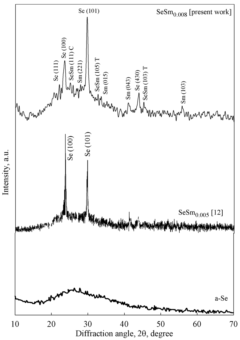 | Figure (1). XRD pattern of a-Se, SeSm0.005 [12] and SeSm0.008 (present work) films prepared by thermal evaporation. The pattern shows the amorphous character for a-Se while for SeSm0.005, the spectrum illustrates also the amorphous nature with presence of some crystallites zones. Furthermore, the polycrystalline nature of SeSm0.008 is shown |
3.1. Dispersion of the Electrical Admittance
- In ac electrical conductivity, semiconductors exhibit a peculiar dependence on frequency as shown in Fig. (2). This figure demonstrate the real part of the admittance, Y' as function of frequency, f, plotted at isotherms 311, 250, 200, 150 and 100 K. It should be noted that, for clarification purpose, not all the recorded temperature data points are depicted in the figure.
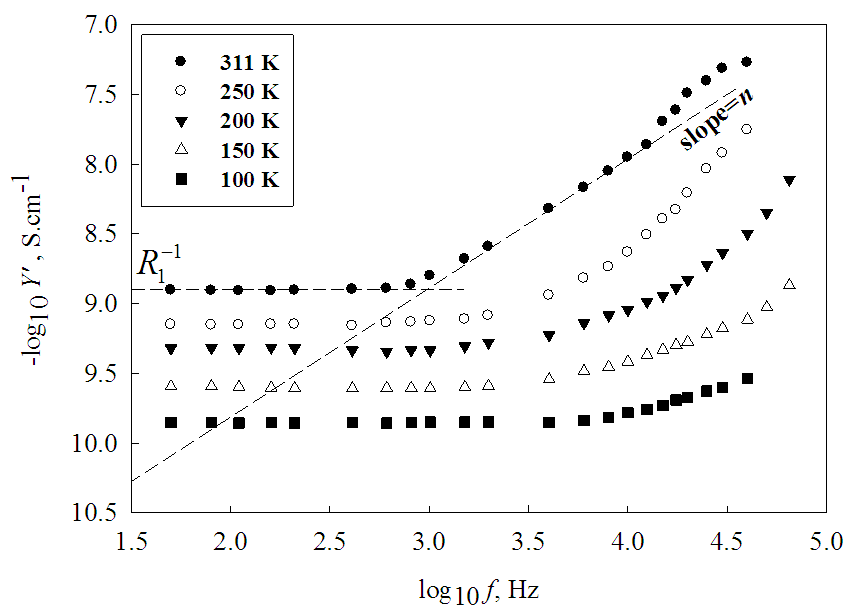 | Figure (2). Spectroscopic plot of log Y ' against log f at different isotherms. The plot illustrates that at each temperature there are two distinct regions at low and a high frequency for the studied films |
 | (1) |
 Furthermore, in the low frequency range and at each temperature the function log Y' against log f are fitted locally point by point to horizontal linear regression line. The extrapolation of the fitted line intersect Y' -axis to give the reciprocal of the initial value of the dc resistance (R1) of the studied sample [15].In the high frequency region of Fig. (2), the admittance increases linearly against the frequency indicating the deviation of the impedance data from ideal 'Debye like' behavior. In order to model non-ideal IS data of this region, a constant phase element (CPE) is used in addition to resistor and capacitance. The impedance of CPE
  is defined as [10]:
 | (2) |
 is the extrapolated intercept with the log Y' axis. The value of n (0 ≤ n ≤ 1) serves as evidence for the type of the dominant ac conduction mechanism in the studied material [16, 7]. The equivalent circuit model enables to analyze and characterize electrically different active regions in the studied material in which the responses of these regions could be deconvoluted and characterized separately. The equivalent circuits are composed of combinations of the impedances of the different structural regions of the studied material besides the CPE in case of deviation from Debye's model.
3.2. Evaluating the Initial Values of Impedances of the Basic Equivalent Circuits
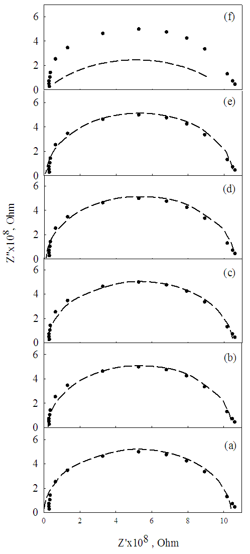
- To apply the equivalent circuit approach, the numerical values of the impedances Z1 (R1-C1) and Z2 (R2-C2-CPE) corresponding to the two structural areas of the films must be evaluated as follows: The impedance spectrum in a complex plane for the studied SeSm0.008 is shown in Fig. (3) at temperatures 311, 250 and 100 K. Presence of one semicircle at each temperature in Fig. (3) means that we have two resistance where the higher one is more pronounced than the other. The experimental data shown in Fig. (3) are fitted using the most simple equivalent circuit R1║C1-R2║C2 (inset of Fig. (3)) which is represented numerically by following equations [15, 17]:
 | (3) |
 | (4) |
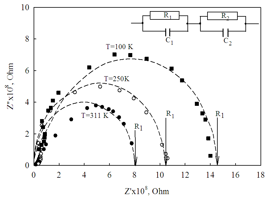 | Figure (3). The impedance spectrum of the investigated films at 100, 250 and 311 K in the complex plane. The symbols correspond to experimental data while dashed lines represent the fitting using the equivalent circuit shown in the inset |
 | (5) |
 | (6) |
 | (7) |
 | (8) |
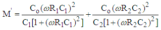
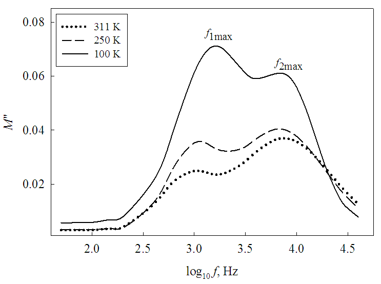 | Figure (4). A plot of imaginary part of the electrical modulus, M", as function of frequency for the studied SeSm0.008 films at different temperatures |
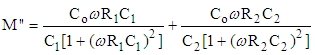
 By applying eq. (8) R2 could be also determined.
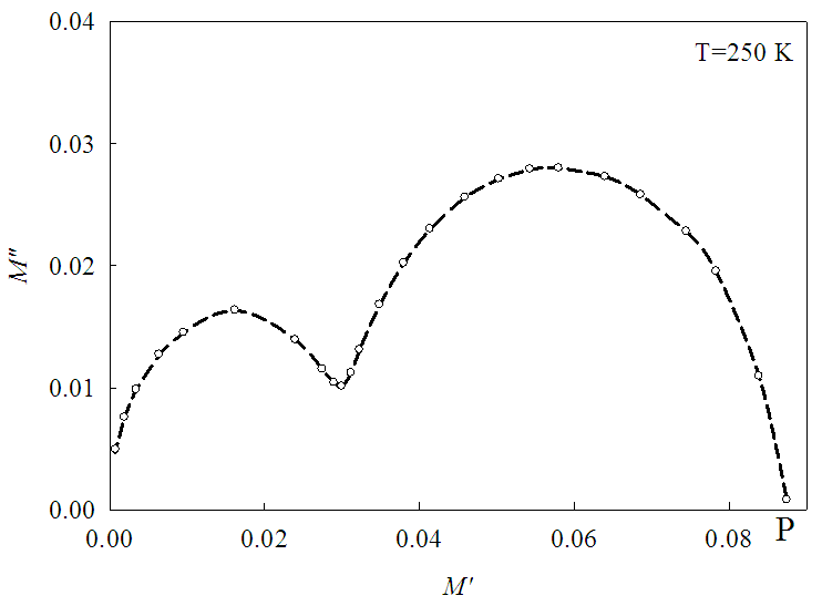 | Figure (5). Spectroscopic plot of M" against M' at T=250 K. The symbols correspond to experimental data while dashed line represents the fitting using the equivalent circuit shown in the inset of Fig. (3) for the studied samples |
3.3. Modeling of the Impedance Data Using Equivalent Circuit approach
- Besides the basic circuit, with two parallel RC elements (inset of Fig. (3)), a more five equivalent circuits with CPE elements have been chosen for the purpose of modeling impedance characteristics for SeSm0.008 thin films. The proposed electrical circuits are shown in Fig. (6) while the expression for total impedance Z* for each circuit is given elsewhere [7, 18].
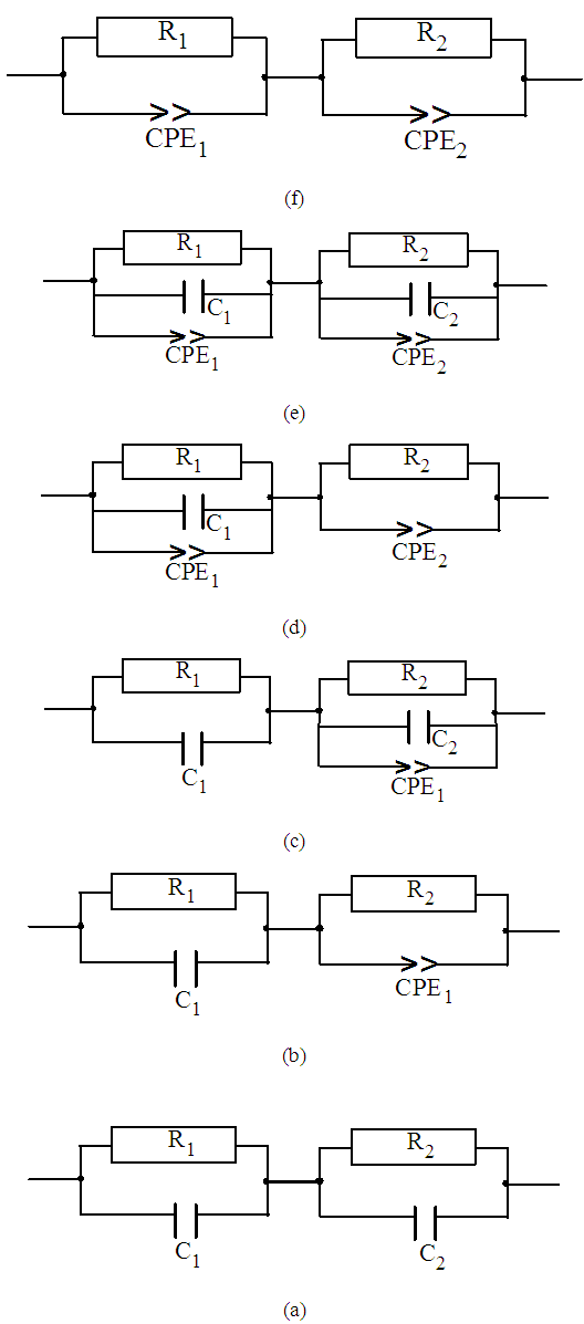 | Figure (6). Various proposed equivalent circuits used to model IS data of the studied films |
 | Figure (7). Measured (closed circles) and best fit (dashed lines) complex-plane impedance plots at 250 K for the present SeSm0.008 films using the proposed equivalent circuits shown in Fig. (6). The sequence of the subfigures in Fig. (7) has the same meaning as in Fig. (6) |
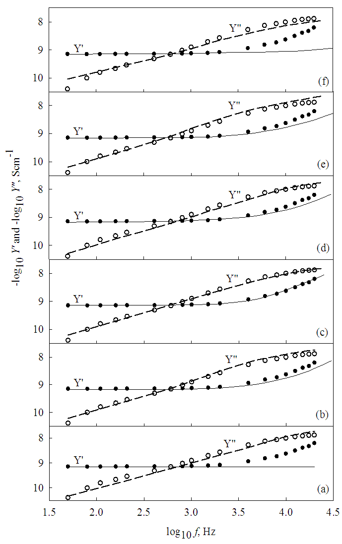 | Figure (8). Measured Y' (solid circles), Y” (open circles) at 250 K and the best fit of Y' (solid lines) and Y" (dashed lines) spectroscopic plot as function of frequency for SeSm0.008 films using the proposed equivalent circuits shown in Fig. (6). The sequence of the subfigures in Fig. (8) has the same meaning as in Fig. (6) |
3.4. Investigation of Electrical Conduction Mechanisms
3.4.1. a.c. conduction
- The fitting process to select the most appropriate circuit (sec. 3.3) yielded an adjustable and final value of the basic elements of circuit c (see figures 7 and 8). The values of the exponent n as calculated in the high frequency region of Fig. (2) and in the considered temperature range, is shown in Fig (9) as an open triangles.
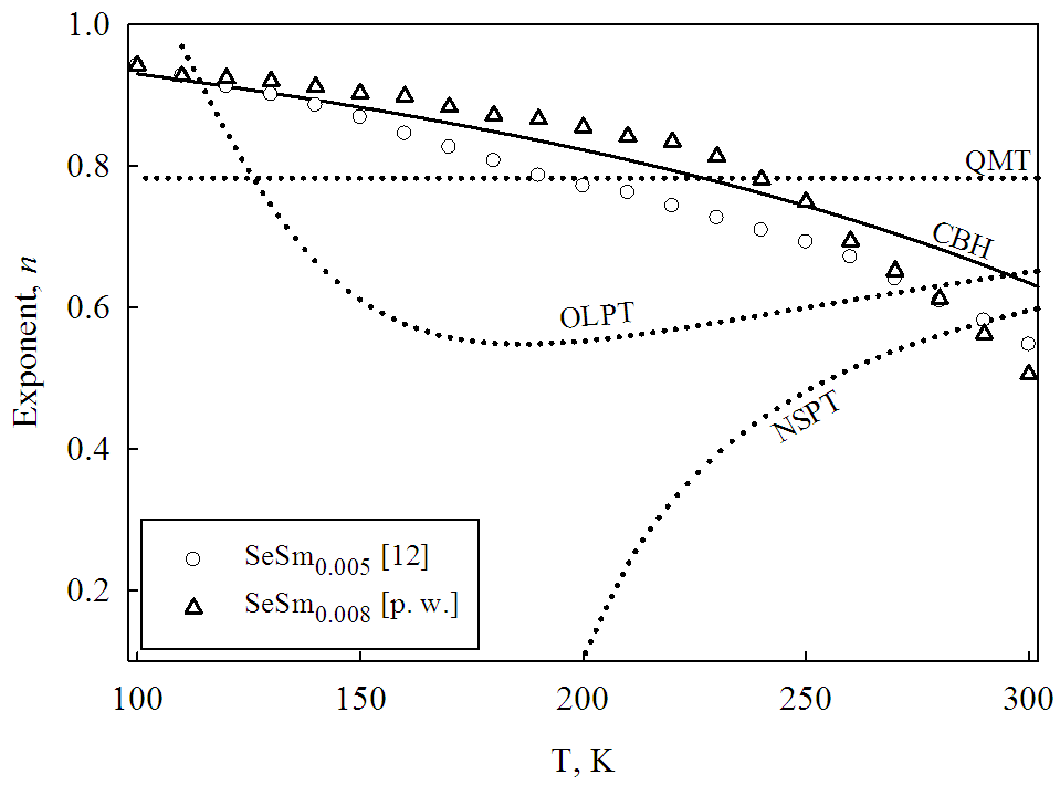 | Figure (9). Temperature dependence of the frequency exponent n for the present work [p. w.], together with the previous published work [12]. The dotted curves represent the values calculated using the models: QMT [21], NSPT [21], OLPT [22] and CBH [23, 24] |
 | (9) |
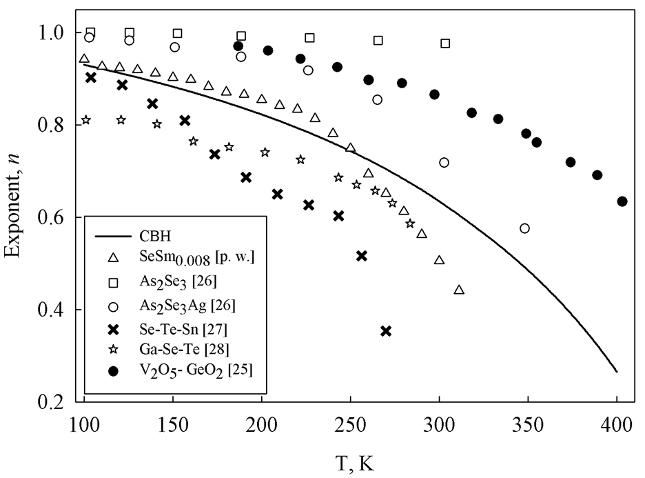 | Figure (10). Temperature dependence of the frequency exponent n for the present work and other chalcogenide systems previously published in the literature for instance As2Se3 [26], As2Se3Ag [26], Se-Te-Sn [27], Ga-Se-Te [28] and also oxide glasses which behaves as semiconductor such as V2O5-GeO2, [25]. The solid curve represents the theoretical values of n calculated using CBH model (Eq. 9)) |
3.4.2. dc conduction
- The adjustable and final values of the resistances R1 and R2 together with the thickness of the sample and contact area of the studied film are used to calculate the dc conductivity in the studied temperature range (311-100 K) as shown in Fig (11).
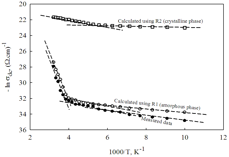 | Figure (11). Temperature dependence of the dc conductivity, calculated using the amorphous, R1, and crystalline, R2, resistances for the present films. The measured conductivity of the same samples is also inserted in the figure for comparison. The symbols correspond to experimental data while dashed lines represent the fitting using linear regression |
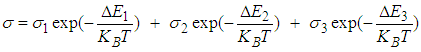 | (10) |
4. Conclusions
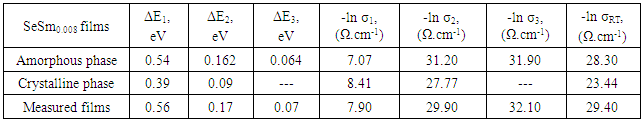
- A detailed application of impedance spectroscopy approach on the effect of Sm doping to a-Se and polycrystalline SeSm0.008 thin films, prepared by thermal evaporation, in the temperature 311–100 K and frequency 50 Hz–80 kHz ranges allows drawing the following conclusions:1. The spectroscopic plot of the real part of the admittance as function of frequency showed an independent plateau (dc component) followed by a "cross over" region to high frequency dispersion (ac component) where log Y' increases linearly with log f. This trend illustrates presence of two micro-structure phases in the structural network of the studied film which is also confirmed by x-ray diffraction pattern. 2. In the low frequency section where Debye model is obeyed the microstructure are represented by R║C elementary circuit. Indeed, in the high frequency region the deviation from Debye trend is observed and the structure could be represented electrically by simple R║C and constant phase element, CPE. 3. The complex plot of Z'-Z", M'-M" and Z",M" as function of the frequency are used to calculate the initial values of the basic elements of the circuits R1, R2, C1, C2 and impedance elements (n and A) for CPE. 4. A comparison between the theoretical values of the index n calculated using the current a.c. conduction models together with that obtained by applying the equivalent circuit approach in the high frequency range proved that correlated barrier hopping (CBH) is the most probable model to represent the a.c. conduction mechanism for the studied films.5. Using the initial values as fitting parameters, the theoretical trend of the complex plot of Z'-Z" for all equivalent circuits together with the experimental results are calculated. Such a comparison revealed that equivalent circuit which is composed of R1║C1 connected in series with R2║C2║CPE is fairly good to represent the micro-structure of the studied films over the whole studied frequency range. 6. The σdc of amorphous phase calculated using R1 shows three distinct conduction while in the case of crystalline phase which is evaluated using R2 shows only two conduction mechanisms.7. The variation of the capacitances C1 and C2 lie in the limits (0.5-2.4) x 10-12 F and (1.54-2.7) x 10-12 F for amorphous and crystalline phases in sequences in the temperature 311-100 K. which is also observed in other chalcogenide compositions.
References
| [1] | M. Kastner, Bonding bands, Lone pair bands and Impurity states in Chalcogenide Semiconductors, Phys. Rev. Lett. 28 (1972) 355-357. |
| [2] | V.N. Antonov, B.N. Harmon and A.N. Yareska, Electronic structure of mixed-valence semiconductors in the LSDA+U approximation. I. Sm monochalcogenides, Phys. Rev. B 66 (2002) 165208-1-165208-10. |
| [3] | H.S. Wio, B. Aloscio, and A. López, Phase diagram of samarium monochalcogenides, Sol. Stat. Commun. 15 (1974) 1933-1936. |
| [4] | A. Svane, G. Santi, Z. Szotek, W.M. Temmerman, P. Strange, M. Horne, G. Vaitheeswaran, V. Kanchana, L. Petit and H. Winter, Electronic structure of Sm and Eu chalcogenides, Physica Status Solidi B 241 (2004) 3185-3192. |
| [5] | B.G. Elmegreen, G. Bruce, K.L. Elbaum, L.X. Hu, J.G. Martyna, M. Muser, M.D. Newns, Piezo-driven non-volatile memory cell with hysteretic resistance, US patent application, Application Number: 12/234100, Filing Date: 09/19/2008. |
| [6] | V. V. Kaminskii, S. M. Solov’ev, A. V. Golubkov, Electromotive Force Generation in Homogeneously Heated Semiconducting Samarium Monosulfide, Technical Physics Letters 28 (2002) 229-231. |
| [7] | D. Mancic, V. Paunovic and Z. Petrušic, Application of Impedance Spectroscopy for Electrical Characterization of Ceramics Materials, Electronics 13 (2009) 11-17. |
| [8] | D.C. Sinclair, Characterization of Electro-materials using ac Impedance Spectroscopy, Bol. Soc, Esp. Cerám. Vidrio 34 (1995) 55-65. |
| [9] | V. Tudic, AC Impedance Spectroscopy of a-nc-Si:H Thin Films, Engineering 6 (2014) 449-461. |
| [10] | E.J. Abram, D.C. Sinclair and A.R. West, A Strategy for Analysis and Modelling of Impedance Spectroscopy Data of Electroceramics: Doped Lanthanum Gallate J. Electroceramics 10 (2003) 165-177. |
| [11] | F.A. Abdel-wahab, H.M. Maksoud and M.F. Kotkata, Electrical conduction and dielectric relaxation in semiconductor SeSm0.005, J. Phys. D: Appl. Phys. 39 (2006) 190-195. |
| [12] | M.F. Kotkata, F.A. Abdel-Wahab and H.M. Maksoud, Investigations of the conduction mechanism and relaxation properties of semiconductor Sm doped a-Se films, J. Phys. D: Appl. Phys. 39 (2006) 2059-2066. |
| [13] | R. Suryanarayanan and C. Paparoditis, Preparation of rare earth chalcogenide thin films by the co-evaporation technique, J. Cryst. Growth 13/14 (1972) 389-392, ibid, Photoconductivity in SmSe, Phys. Lett A. 42 (1973) 373-374. |
| [14] | R.B. Bekeen and J.W. Schweitzer, Intermediate valence in alloys of SmSe with SmAs, Phys. Rev. B 23 (1981) 3620-3626. |
| [15] | A.R. West, D.C. Sinclair and N. Hirose, Characterization of Electrical Materials, Especially Ferroelectrics, by Impedance Spectroscopy, J. Electroceramics 1 (1997) 65-71. |
| [16] | A.N Papathanassiou, The power law dependence of the a.c. conductivity on frequency in amorphous solids, J. Phys. D: Appl. Phys. 35 (2002) L88- L89. |
| [17] | D.C. Sinclair and A.R. West, Impedance and modulus spectroscopy of semiconducting BaTiO3 showing positive temperature coefficient of resistance, J. Appl. Phys. 66 (1989) 3850-3856. |
| [18] | M.E. Orazen, B. Tribollet, Electrochemical impedance spectroscopy. John Wiley & Sons, Inc., USA, 2008. |
| [19] | A.K. Jonscher, The universal dielectric response, Nature 267 (1977) 673-679. |
| [20] | N.F. Mott and E.A. Davis, Electronic Processes in Non-Crystalline Materials, 2nd edn Clarendon Press, Oxford, 1979. |
| [21] | A. Ghosh, Frequency-dependent conductivity in bismuth-vanadate glassy semiconductors, Phys. Rev. B 41 (1990) 1479-1488. |
| [22] | R. Long, Frequency-dependent loss in amorphous semiconductors, Adv. Phys. 31 (1982) 553-637. |
| [23] | S.R. Elliot, A.c. conduction in amorphous chalcogenide and pnictide semiconductors, Adv. Phys. 36 (1987) 135-218. |
| [24] | S.R. Eilliot, A theory of a.c. conduction in chalcogenide glasses, Phil. Mag. B 36 (1977) 1291-1304. |
| [25] | A. Ghosh, Transport properties of Vanadium germanate glassy semiconductors, Phys. Rev. B 42 (1990) 5665. |
| [26] | F. Abdel-Wahab, Signature of the Meyer–Neldel rule on the correlated barrier-hopping model, J. Appl. Phys. 91 (2002) 265-270. |
| [27] | F. Abdel-Wahab, A.A. Montaser, A. Yelon, Mechanism of ac and dc conduction in chalcogenide glasses, Monatsh Chem. 144 (2013) 83–89. |
| [28] | A.S. Maan, D.R. Goyal and A. Kumar, A.C. conductivity of amorphous Ga-Se-Te system, Revue De Phys. Appl. 24 (1989)1071-1075. |
| [29] | A. Kumar, M. Lal, K. Sharma, P.S. Gill, and N. Goyal, Dielectric properties of Se85-xTe15Gex chalcogenide glasses, chalcogen Lett. 11 (2014) 249-256. |
| [30] | T. Suntola, O.J.A. Tiainen and M. Valkiainen, Differential capacitance of chalcogenide thin films, Thin Solid Films 14 (1972) S3-S5. |
| [31] | S. Gautam, A.Thakur, S.K. Tripathi and V. Goyal, Effect of silver doping on the electrical properties od a-Sb2Se3, J. Non-Cryst. Solids 353 (13-15) (2007) 1315-1321. |
| [32] | N. Chaoudhary and A. Kumar, Dielectric relaxation in glassy Se70Te30-xAgx, Indian J. Pur. & Appl. Phys. 44 (2006) 62-65. |
| [33] | S. Wagle and V. Shirodkar, Dielectric Properties of thin Film Al/Sb2Pb1Se7/Al Devices, Brazil. J. of Phys. 30 (2000) 554-559. |