-
Paper Information
- Paper Submission
-
Journal Information
- About This Journal
- Editorial Board
- Current Issue
- Archive
- Author Guidelines
- Contact Us
American Journal of Condensed Matter Physics
p-ISSN: 2163-1115 e-ISSN: 2163-1123
2016; 6(2): 21-26
doi:10.5923/j.ajcmp.20160602.01

Electrical Characteristics of Zn Doped In2Se3 Thin Films for Phase Change Memory (PRAM) Applications
 Abstract
 Reference
 Full-Text PDF
 Full-text HTML
Opiyo S. O., Munji M. K., Njoroge W. K., Makori N. E., Obare B. M.
Department of Physics Kenyatta University, GPO Nairobi, Kenya
Correspondence to: Opiyo S. O., Department of Physics Kenyatta University, GPO Nairobi, Kenya.
| Email: |  |
Copyright © 2016 Scientific & Academic Publishing. All Rights Reserved.
This work is licensed under the Creative Commons Attribution International License (CC BY).
http://creativecommons.org/licenses/by/4.0/

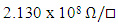
The effects of Zinc doping on electrical characteristics of In2Se3 for PRAM applications have been successfully investigated. The results obtained show an increase in sheet resistance for as deposited and annealed films with increase in Zn doping. In-situ electrical properties during thermal cycling showed a sharp drop in sheet resistance showing a transition from amorphous to crystalline phase. Zinc doping also affected the resistance contrast with the highest contrast found to be  for 4% Zn doping. Crystallization temperature increased linearly with zinc doping. From the study, 4% Zn doping gave the best results for PRAM fabrication as it registered moderately high crystallization temperature as well as high resistance contrast. These properties ensure stability of the cell as well as reduce the RESET current. The PRAM fabricated from 4% Zn doped sample, registered a threshold voltage of 4.60V during I-V testing. The pulsed mode testing resulted in a SET pulse of 2.38V, 15μs and a RESET pulse of 4.75V, 75ns. The obtained threshold voltage of 4.6V suggests that the material is scalable.
Keywords: Indium Selenide (In2Se3), Phase Change Random Access Memory (PRAM), Current Voltage (I-V) test
Cite this paper: Opiyo S. O., Munji M. K., Njoroge W. K., Makori N. E., Obare B. M., Electrical Characteristics of Zn Doped In2Se3 Thin Films for Phase Change Memory (PRAM) Applications, American Journal of Condensed Matter Physics, Vol. 6 No. 2, 2016, pp. 21-26. doi: 10.5923/j.ajcmp.20160602.01.
Article Outline
1. Introduction
- Phase Change Random Access Memory (PRAM) is one of the most promising concepts for the future generations of Non Volatile Memories. Generally PRAM is a non-volatile memory that employs the reversible phase change in material to store bits of information [1]. PRAM utilizes the large resistivity contrast between crystalline (low resistivity) and amorphous (high resistivity) phases of the Phase Change Material (PCM). The SET and the RESET states of the PRAM refer to low and high resistance respectively. The operation speed of PRAM is limited by the SET programming time because it takes finite time to fully crystallize the amorphous region. This idea of using amorphous to crystalline phase transition of chalcogenides for an electronic memory technology has been pursued for many years [2]. PRAMs have desirable characteristics including; fast switching speed, low programmable energy, high endurance, good data retention, improved compatibility with CMOS and excellent scalability [3]. Studies have also shown that PRAM cycling endurance is of the order 108 writes (the number of successive write/erase cycles before the cell fails) which is significantly higher than that of floating gate technology which is reported to be approximately 105 [4]. In addition PRAM is capable of creating new functions and applications of its own which are fast write programming speed and direct overwrite capability [5].Many researchers have widely studied Ge2Sb2Te5 (GST) and optimized it for PRAM applications. However GST has been reported to have some drawbacks for instance, meta-stable face centered cubic (fcc) structure, low crystallization temperature and low crystallization resistance. The low crystallization temperature means it is unable to retain data at high temperature. To eliminate these problems, anew PCM for next generation PRAM applications must have a higher crystallization temperature and also higher crystalline resistance with a faster phase change speed than GST. Research has shown that crystallization temperature is directly proportional to the data stability while crystalline resistance is inversely proportional to the RESET operation power [6]. It is therefore necessary to come up with a material that has high crystallization temperature and also high crystalline resistance. This will ensure an improved data retention capability and reduce the RESET power of the PRAM. Additives for instance Zinc, Silicon dioxide, Titanium, Nitrogen among others have been reported to have the ability to influence the crystallization temperature of PCM. Addition of carbon has been found to lead to an increase in crystallization temperature and activation energy for crystallization of GeTe [7, 8]. Selenium has been found to have tremendous potential in device technology since it exhibits a unique property of reversible transition. Additives increase the hardness, sensitivity and crystallization temperature of selenium as well as lessening the ageing effect [9]. This study was aimed at finding out the effect of Zn additive at lower percentages (0-8%) on the electrical characteristics of In2Se3 for PRAM application.
2. Experimental Procedures
2.1. Zn:In2Se3 Alloys Synthesis and Thin Film Deposition
- Elements of In and Se granules, of purity 99.999% were synthesized in the ratios of 2:3 by atomic mass. Zn of similar purity was then introduced into the sample at different ratios (0%-8%, in steps of 2%) by mass. The composition was then loaded in Pyrex glass tube and then sealed before heating to about 450°C in the presence of argon. During heating there was slight shaking of the tube to obtain homogeneity. The obtained homogenous solid alloy was ground in a porcelain motor. Edward Auto 306 RF/DC evaporation chamber was employed in the thin film deposition. Thoroughly cleaned ordinary microscope glass slides were used as substrates and mounted on the chamber substrate holder. The chamber pressure was then pumped down to 3.0 x 10⁻⁵ mbar pressure at room temperature. A current of 3A was used to heat up the boat to allow for the evaporation of the sample and a final thin film deposition on the substrate.
2.2. Sheet Resistance Determination during Thermal Cycling
- The sheet resistance of the sample was obtained at various temperatures (ranging from 25°C to 300°C in steps of 5°C). During thermal cycling, Lindberg Mini-Mite TF55035Atube furnace was used for annealing. Keithley 2400 sourcemeter in four wire mode was used to determine the I-V characteristics of the films the temperature was ramped at a constant rate of 10K/minute [10]. To eliminate chances of oxidation of the film, Argon gas was flown through the Lindbergh furnace continuously at a constant rate of 1sccm.
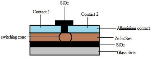 | Figure 1. Schematic diagram of PRAM cell |
2.3. Fabrication of a PRAM
- A PRAM was fabricated by depositing first a layer of SiO2 on a clean normal glass substrate. This was followed by a layer of Zn:In2Se3. Aluminum strip of width 1 mm was used to mask the switching zone on the PCM before depositing a thin film of Aluminum to form the two contacts (1 and 2) as shown in figure 1. A further layer of SiO2 was deposited to passivate the switching zone. All the layers were 100nm thick as that was the optimum thickness. The method of deposition for all the layers was evaporation technique.
2.4. Characterization of the PRAM
2.4.1. DC Current Sweep Test
- DC test was achieved by connecting the PRAM in series with 1 kΩ resistor and a 60V variable voltage supply. Keithley 2400 Sourcemeter was used to measure current through the cell while the digital multimeter was used to determine voltage across the cell. Voltage values were determined while the current was varied from 0 to 5 mA in steps of 0.01mA.
2.4.2. Pulsed Mode Test
- For pulsed mode testing Agilent 81104 pulse generator was employed. The pulse width (time) was set at 75ns and 15μs for RESET and SET operations respectively.During RESET operation voltage was varied from 1V to 6V while in the SET operation the voltage was varied from 1V to 3V.
3. Results and Discussions
3.1. Thermal Cycling
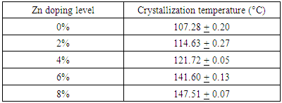
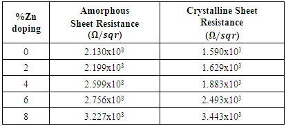
- Figure 2 shows variation of sheet resistance of the as deposited Zn:In2Se3 thin films with temperature. From the graph, the gradual decrease in sheet resistance at lower temperatures and sudden drops in the sheet resistance at specific temperatures values are observed. The specific temperature values where the sudden drops in sheet resistance occur correspond to the crystallization temperatures of the films [11, 12]. The minima of Gaussian fits of the derivative of R-T graph results gave crystallization temperatures as shown in table 1 below.
|
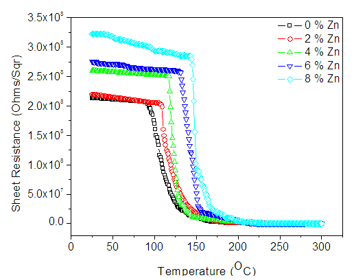 | Figure 2. R-T curves of In2Se3 doped with different (%) concentration of Zn |
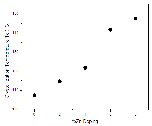 | Figure 3. Variation of crystallization temperature with % Zinc doping |
|
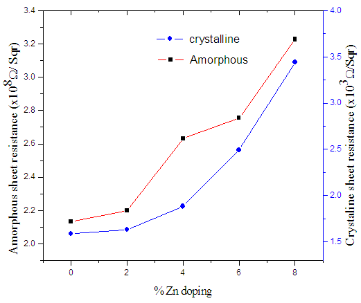 | Figure 4. Variation of amorphous/crystalline resistance with %Zn doping levels |
 and
and 
 for 0% Zn and 8% Zn doping respectively. The increase in sheet resistance may be attributed to the disruption of coordination of the atoms of In2Se3 as the zinc doping increases.It’s clear from figure 4 that there is a slight change in sheet resistance at lower zinc percentages (0-4%) after which there is a larger change at higher zinc doping (6-8%). This behaviour may be attributed to non-uniform crystallinity or poor crystallinity at high zinc doping levels. The stability of data in a memory cell is not only a function of the crystallization temperatures of the material of the cell, but also the resistance contrast (ratio of the amorphous to crystalline sheet resistance).
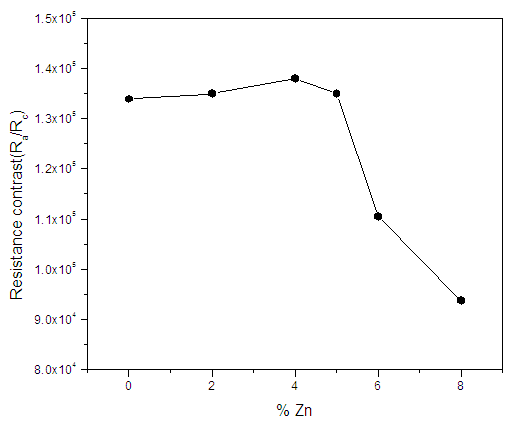 | Figure 5. Graph of resistance contrast with increase in % Zn doping on In2Se3 |
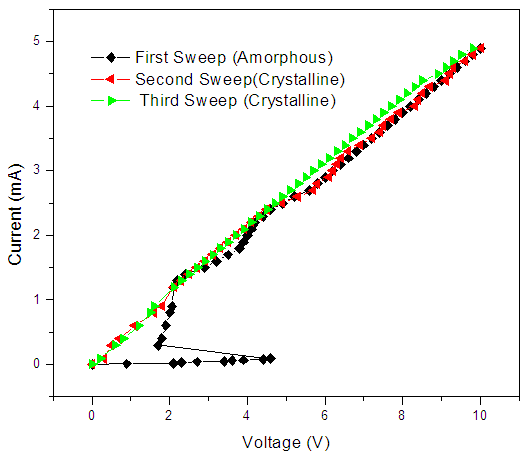 | Figure 6. I-V curve for 4%Zn-In2Se3 PRAM |
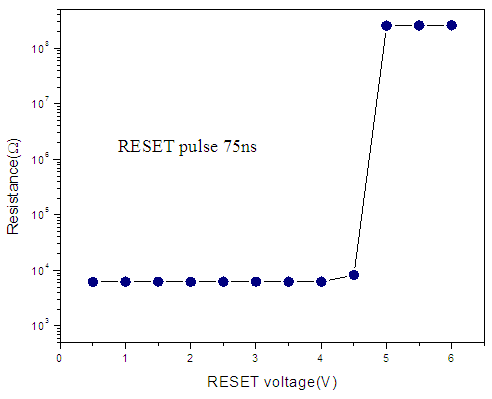 | Figure 7. RESET Pulsed-mode switching behavior of Zn:In2Se3 PRAM |
 for voltages less than 2V. However, at 2.38V the resistance of the cell drastically dropped from 8 orders to 3 orders of magnitude. This voltage is called the SET voltage as the switching region is set to low resistance. This phenomenon occurs due to joule heating of the switching area hence creating a conduction path that switches the material from highly resistance to low resistance.
 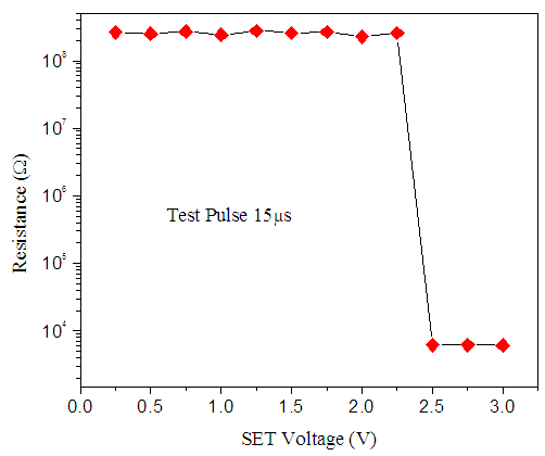 | Figure 8. SET pulsed-mode switching behavior of Zn:In2Se3 PRAM |
4. Conclusions
- The effect of low percentage Zn doping (0%-8%) on In2Se3 thin films for phase change memory application has been successfully investigated in this work. Zn doping raised both amorphous and crystalline sheet resistance of In2Se3 thin film. Crystallization temperature also increased with increase in Zinc doping from 107.28°C to 147.51°C for 0% to 8% doping levels respectively. This indicated an increased stability of the thin films with Zn doping. Four percent (4%) Zn:In2Se3 registered the highest amorphous/crystalline resistance contrast indicating reduced noise in the PRAM as well as considerable increase in stability. The I-V characterization of the PRAM resulted in a threshold voltage of 4.60V while the pulsed mode test yielded a RESET pulse of 75 ns, 4.75V and a SET pulse of 15μs, 2.38V.
ACKNOWLEDGEMENTS
- We would want to say special thanks to the Vice Chancellor Kenyatta University, Prof. Olive Mugenda for availing laboratory resources and for creating an ample environment for science research. Thanks to entire staff of physics department, Kenyatta University lead by the chairman Dr. Walter Njoroge (2011-2015) for their continuous guidance in the laboratory during experiments as well as during the departmental seminars. They surely played a major role in the success of this work.