-
Paper Information
- Paper Submission
-
Journal Information
- About This Journal
- Editorial Board
- Current Issue
- Archive
- Author Guidelines
- Contact Us
American Journal of Condensed Matter Physics
p-ISSN: 2163-1115 e-ISSN: 2163-1123
2016; 6(1): 1-6
doi:10.5923/j.ajcmp.20160601.01

Optical and Electrical Characterization of CuO Thin Films as Absorber Material for Solar Cell Applications
 Abstract
 Reference
 Full-Text PDF
 Full-text HTML
K. S. Wanjala1, W. K. Njoroge1, N. E. Makori1, J. M. Ngaruiya2
1Department of physics, Kenyatta University, Nairobi, Kenya
2Department of physics, Jomo Kenyatta University of Agriculture and Technology, Nairobi, Kenya
Correspondence to: K. S. Wanjala, Department of physics, Kenyatta University, Nairobi, Kenya.
| Email: |  |
Copyright © 2016 Scientific & Academic Publishing. All Rights Reserved.
This work is licensed under the Creative Commons Attribution International License (CC BY).
http://creativecommons.org/licenses/by/4.0/

Copper oxide thin films were deposited on ordinary glass substrates using sputtering technique. The chamber pressure was maintained at 5.0 x 10⁻⁵mbars during the film deposition. The influence of deposition power on electrical and optical properties was extensively investigated. The optical measurements were done using spectrophotometer. Transmittance spectra data in the range 250-2500 nm was obtained and analyzed. Transmittance ranged between 55% to 70% and reflectance of less than 40% in the wavelength range of 250-2500nm was obtained. Optical energy band gap ranged between 1.20-2.91eV. The band gaps generally decreased with increase in power from a deposition power of 100W to 300W, then a slight rise at 350W and 400W. The electrical resistivity decreased steadily with increase in sputtering power from 119 Ω-cm to 37.83 Ω-cm corresponding to powers of 100W and 400W respectively. From the band gap energy values, it was deduced that both CuO and Cu2O films were deposited. Optical and electrical values exhibited by the films deposited at 350W and 400W deposition power, are in the required range for the application of the films as absorber layer in solar cell application.
Keywords: Sputtering, Transmittance, Reflectance, Electrical Characterization
Cite this paper: K. S. Wanjala, W. K. Njoroge, N. E. Makori, J. M. Ngaruiya, Optical and Electrical Characterization of CuO Thin Films as Absorber Material for Solar Cell Applications, American Journal of Condensed Matter Physics, Vol. 6 No. 1, 2016, pp. 1-6. doi: 10.5923/j.ajcmp.20160601.01.
Article Outline
1. Introduction
- CuO is p-type semiconductor which in recent years has attracted much interest due to its potential applications in optical, electro-chromic, gas sensors, and transparent conducting devices [1]. Copper oxide films have unique features such as low cost, non-toxicity, abundantantly available and relatively simple to form oxide layers [2]. Copper oxide has two common forms; cupric oxide (CuO), with a band gap in the range 1.2–2.1 eV and cuprous oxide (Cu2O), with a band gap in the range 2.1–2.6 eV [3]. A number of reports have been made on CuO thin films preparation by various techniques including conventional magnetron sputtering [4], molecular beam-epitaxy method [5], sol-gel technique [6], chemical vapor deposition, spraying, thermal oxidation, electrodeposition [7], among others. To obtain the exact monoclinic CuO crystal structure, high power delivery to the source material during thin film deposition can effectively reduce the dependence of substrate heating to obtain high quality crystal film, such as Pulsed laser deposition [8] and ion-based deposition [9]. This work reports on the preparation and characterization of Copper oxide thin films by sputtering technique. The effect of varying power on the optical and electrical properties of sputtered copper oxide films was investigated with the aim of employing the films for solar cell devices as absorbing layers.
2. Experimental Procedure
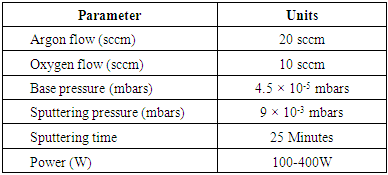
- DC magnetron sputtering machine was used. A copper target (99.99% pure) was sputtered in an Argon/Oxygen ambient. First, transparent glass slides were cleaned then mounted at the centre of the revolving substrate holder. The copper target was then mounted on the magnetron and a shutter covered it. The chamber was then closed and pumped down to a pressure of 4.5×10⁻⁵ mbars. Power was set to 100W and then argon gas let into the chamber at a flow of 20 sccm. With the target still covered, pre-sputtering was done for 10 minutes so as to remove any oxide layers that may be on the target. Once pre-sputtering was complete, Oxygen was allowed into the chamber and the shutter was then opened for 25 minutes allowing copper atoms ejected to rise up towards the substrate. In the process, a reaction between copper atoms and oxygen took place hence forming copper oxide thin films on the substrates. During sputtering, sputter pressure was maintained at 9×10⁻³ mbars by regulating inflow of argon gas. After the films were formed, they were removed, the substrate holder cleaned and other films prepared in the same way at different deposition powers of 150, 200, 250, 300,350 and 400W. Every deposition was preceded by pre-sputtering for 10 minutes. The deposition parameters are summarized in table 1.
|
3. Results and Discussions
3.1. Optical Characterization of CuO Thin Films
- Figure1 shows spectra transmittance of copper oxide films deposited at various deposition powers. A pronounced increase in transmittance is observed for films deposited using deposition powers 350W and 400W. At low wavelengths transmittance is low since energy of photons is high hence being absorbed.
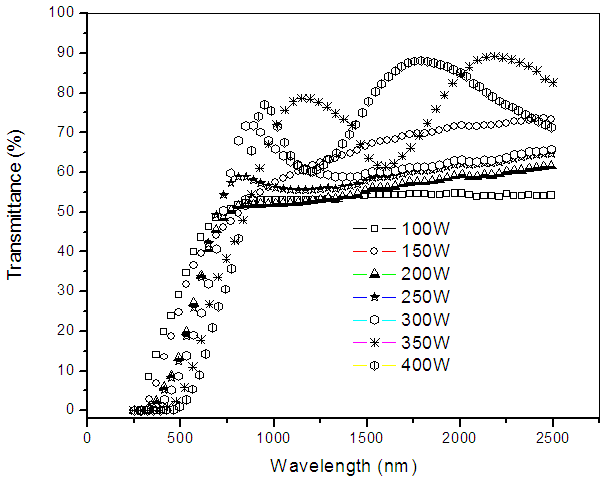 | Figure 1. Spectral plot of transmittance (%) against wavelength (nm) of CuO films deposited using different deposition powers |
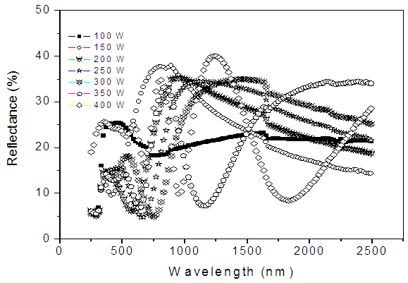 | Figure 2. Spectral plot of reflectance (%) against wavelength (nm) of CuO thin films deposited using different deposition powers |
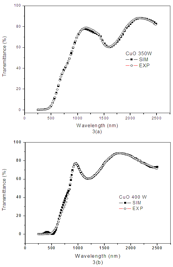 | Figure 3. Transmission simulated curves for CuO thin films deposited at (a) 350W and, (b) 400W |
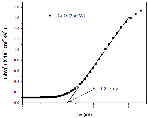 | Figure 4. A plot of (αhν)2 against energy(eV) for CuO, deposited at 350W |
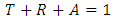 | (1) |
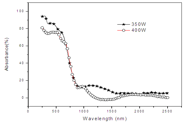 | Figure 5. A plot of absorbance (%) against wavelength (nm) for films deposited at 350W and 400W |
 | (2) |
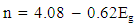 | (3) |
 | Figure 6. A plot of absorbance (%) against wavelength (nm) for films deposited at 350W and 400W |
3.2. Electrical Characterization of CuO Thin Films
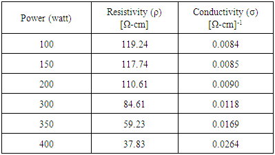
- The effect of power on electrical resistivity of the CuO thin films is shown in figure 7. Electrical resistivity of CuO films was measured in the deposition power range 100-400W. The electrical resistivity is found to decrease steadily to a value of 37.83 for the film prepared at 400W and was in the range 37-119Ω-cm. This decrease in resistivity can be attributed to the dense microstructure at high deposition power which enhances the rapid growth of relatively thick films [13]. The results of the electrical resistivity measurements by [4, 14] followed a similar trend to this present measurement of sheet resistance on copper oxide films and were in the range 10-100 Ω-cm. Low resistivity for films deposited at 350W and 400W make these films suitable for solar cell application.
|
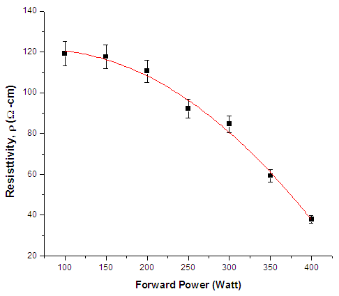 | Figure 7. Electrical resistivity (ρ) against power of CuO films |
4. Conclusions
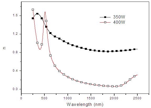
- CuO films were successfully deposited on glass substrate by DC magnetron sputtering at room temperature. The influence of deposition power on CuO thin films was studied. Electrical and optical properties of the deposited thin films have been found to be significantly dependent on power during deposition. The transmittance increased with increase of deposition power of the films. The values of band gap energy in the range 1.20-2.91eV exhibited by the films are in the required range for the application of the films as absorber layer in solar cell fabrication. Refractive index decreased with an increase in deposition power. Resistivity of the films decreased with the increase in deposition power and was in the range of 37-119 Ω-cm.
ACKNOWLEDGEMENTS
- The authors are grateful to the assistance offered by the Physics Department of Kenyatta University where this study was carried out. They also acknowledge the University of Nairobi department of Material Science [Chiromo Campus] for kindly providing the UV-VIS-NIR spectrophotometer 3700 for the spectral analysis of the thin films.