-
Paper Information
- Paper Submission
-
Journal Information
- About This Journal
- Editorial Board
- Current Issue
- Archive
- Author Guidelines
- Contact Us
American Journal of Condensed Matter Physics
p-ISSN: 2163-1115 e-ISSN: 2163-1123
2015; 5(3): 76-79
doi:10.5923/j.ajcmp.20150503.03
Photovoltaic Properties of n-(CdO)1-x(SnO2)x/p-Si Heterojunction Prepared by Pulsed Laser Deposition
 Abstract
 Reference
 Full-Text PDF
 Full-text HTML
Mohammed A. Abdul Majeed1, Nahida B. Hasan1, Ghusson H. Mohammed2
1Department of Physics, Collage of Science, University of Babylon, Babylon, Iraq
2Department of Physics, Collage of Science, University of Baghdad, Baghdad, Iraq
Correspondence to: Mohammed A. Abdul Majeed, Department of Physics, Collage of Science, University of Babylon, Babylon, Iraq.
| Email: |  |
Copyright © 2015 Scientific & Academic Publishing. All Rights Reserved.
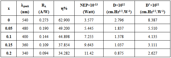
CdO heterojunction can be synthesized and formed into an ultraviolet (UV) photodetector at different concentration of SnO2 (x = (0.0, 0.05, 0.1, 0.15 and 0.2)) Wt. % onto a silicon wafer substrate by pulsed laser deposition technique (PLD) using Nd-YAG laser with λ=1064nm, energy=600mJ and number of shots=500. The spectral response of n-(CdO)1-x(SnO2)x/p-Si was studied. The influence of SnO2 content on the photocvoltaic properties of CdO hetrojunctions is studied The values of responsivity, specific detectivity and quantum efficiency decrease and shift to short wavelength with increase of concentration SnO2. Good photoresponse to UV light has been demonstrated for CdO doped with SnO2 heterojunction photodetectors when increases SnO2 was investigated. A high broad peaks are observed around λ= 550nm for pure CdO and shift to λ=300nm when doping with 0.25 wt SnO2.
Keywords: Heterojunction, CdO films, SnO2 films, Pulsed laser deposition, Photovoltaic properties
Cite this paper: Mohammed A. Abdul Majeed, Nahida B. Hasan, Ghusson H. Mohammed, Photovoltaic Properties of n-(CdO)1-x(SnO2)x/p-Si Heterojunction Prepared by Pulsed Laser Deposition, American Journal of Condensed Matter Physics, Vol. 5 No. 3, 2015, pp. 76-79. doi: 10.5923/j.ajcmp.20150503.03.
Article Outline
1. Introduction
- Cadmium Oxide CdO is unique combination of cardio thin film properties which were represented by high electrical conductivity, high carrier concentrations and high transparency in the visible range of the electromagnetic spectrum, made it suitable for a wide range of applications in different fields [7, 6]. The applications of CdO thin films are in photovoltaic solar cells for front contacts window layer, or as heterostructure such as CdO/CdTe or CdO/Cu2O solar cells [1, 8, 9], Photoelectrochemical devices [3], Phototransistors [3, 5], photodiodes [2, 4], Liquid crystal displays [5, 4], - Antireflection coatings [3], IR detectors [5] and Gas sensors [1-4].- Transparent electrodes was used as transparent anodes for organic light emitting (OLEDS) as a practical new display technology [1, 3]. It has been used as heat mirrors, due to its high reflectance in the infrared region together with transparency in the visible region [4]. Stannic Oxide SnO2 In 1942 Masters [10] succeeded in preparing conductive transparent tin oxide, for the first time. A substance with white color has a molecular weight of (150. 69 g/mol). Its density (6.95 g/cm3), its melting point (1630°C) and its boiling point (1900°C) [11]. Stannic oxide is an n- type semiconducting material with a direct band gap of about 4.0 eV and an indirect band gap of about 2.6 eV [12]. The electron concentration in the conduction band arises primarily from the lack of stoichiometry produced by oxygen deficiency. The property of SnO2 makes the material useful for many applications. There for increasing attention is begin paid to study this oxide especially on the method of operation, and its electrical and optical properties. SnO2 thin films have been fabricated using different techniques including pulse laser deposition, electron beam evaporation [13], chemical vapor deposition [14], RF sputtering [15], evaporation and chemical spray pyrolysis [16]. SnO2 as transparent conducting oxide is used extensively for a variety of applications such as transparent electrodes in solar cells, architectural windows and flat panel displays [17]. Recently SnO2 has been integrated into micro chemical silicon devices as a sensing element of micro sensor.
2. Experimental
2.1. Preparation Pellets
- High purity powders (99.999%) of CdO and SnO2 supplied from Fluka were used to form the target as a disk of 2.5cm diameter and 0.4 cm thickness by pressing it under 4 ton force. The pellets which containing the elements were heated to 873K for 3 hours then cooled to room temperature. The temperature of the furnace was raised at a rate of 10°C/min. The amount of elements content of pellets was evaluated by using the following equation.
 | (1) |
 atomicweight for CdO),
  (atomic weight for SnO2) and x=0, 0.05, 0.1, 0.15 and 0.2 (concentration of SnO2).
 2.2. Preparation of Porous Silicon Layer by Photochemical Etching
- The p-type Si wafer of (0.05 Ω. cm) resistivity was used as a starting substrate in the photochemical etching. The samples of (1.5 × 1.5 cm2) dimensions were cut from the wafer and rinsed with acetone and methanol to remove dirt. The photochemical etching is electrodeless process since there is no applied bias voltage during the etching, this process is carried out by using ordinary light source. The setup consists of a Quartz Tungsten Halogen lamps (250W) integrated with dichroic ellipsoidal mirror supplied from Philips Company, focusing lens and the diluted etching acid in container.. In order to remove the native oxide layer on the samples, they were etched in diluted (10%) HF acid. After cleaning the samples they were immersed in HF acid of 50% concentration and ethanol 50% in a container. The light source was vertically mounted by a holder above the sample, aligned and focused by Quartz lens of (3.87cm) focal length to form a circular spot with a suitable power density. The lens was mounted on a driven holder for precise focusing adjustment. The distance from the lamp to the lens was about 30 cm and from the lens to the sample 14 cm. The PS was formed on the illuminated side of the sample. The photo etching irradiation times was chose to be about 10 minutes.At the end of the photochemical etching process, the sample were rinsed with ethanol and stored in a glass containers filled with methanol to avoid the formation of oxide layer above the nanospikes thin film. The nanospikes silicon layers were used as a substrate for (CdO)1-x(SnO2)x the photoconductive detector elements.
2.3. Thin Film Preparation and Chractrazation
- The (CdO)1-x(SnO2)x heterojunction were deposited porous silicon wafers of (100) orientation were used in this work heterojunction at room temperature by PLD technique using Nd:YAG with λ = 1064 nm SHG Q-switching laser beam at 600 mJ, repetition frequency (6Hz) for 500 laser pulse is incident on the target surface making an angle of 45°. The under vacuum of (10−3mbar) at room temperature. DC power supply (0-15V, 0-2 A), a variable resistance is used to limit the detector bias current. A PC-interfaced digital Multimater and Laptop PC are used to register the output circuit current. The UV – Led is used as a UV source for illumination of the CdO: SnO2 photoconductive UV detector. The optical power of the UV Led is 2.5mW and the wavelength is about 385 nm.
3. Results and Discussion
3.1. Spectral Measurements for (CdO)1-x(SnO2)x/p-Si Heterojunction
3.1.1. Spectral Responsivity (Rλ)
- Spectral responsivity (Rλ) is the most important parameter by which the range of hetrerojunction operation can be determined using equation [18].
 | (2) |
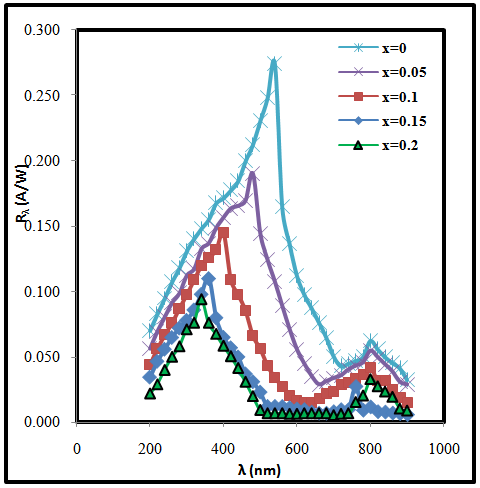 | Figure (1). The variation of responsivite (Rλ) with the wavelength for (CdO)1-x(SnO2)x/p-Si heterojunction with different concentration of SnO2 |
3.1.2. Noise Equivalent Power
- The noise equivalent power (NEP) values were calculated using equation [18].
 | (3) |
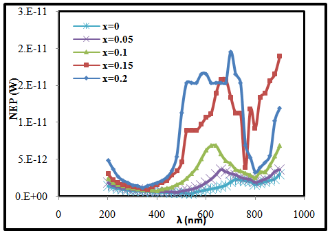 | Figure (2). The variation of noise equivalent power with the wavelength for (CdO)1-x(SnO2)x heterojunction with different concentration of SnO2 |
|
3.1.3. The Specific Detectivity
- The specific detectivity (D*) was calculated using equation [19].
 | (4) |
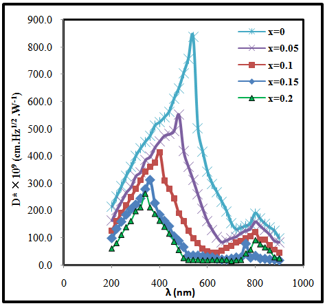 | Figure (3). The variation of Specific Detectivity with the wavelength for (CdO)1-x(SnO2)x/p-Si heterojunction with different concentration of SnO2 |
3.1.4. Quantum Efficiency (η %)
- The quantum efficiency (η) is a very important parameter were calculated using equation [19].
 | (5) |
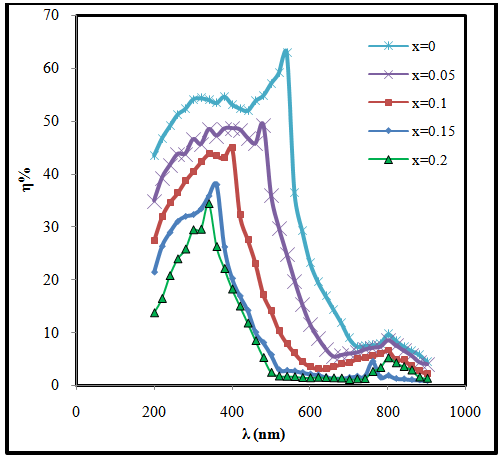 | Figure (4). The variation of quantum efficiency with the wavelength for (CdO)1-x(SnO2)x/p-Si heterojunction with different concentration of SnO2 |
4. Conclusions
- In conclusion, the CdO photovoltaic UV detector was developed using different concentrations of SnO2 prepared by pulsed laser deposition technique. This device exhibits a prominent performance for UV light detection. The spectral response, specific detectivity and quantum efficiency of (CdO)1-x(SnO2)x heterojunction were investigated. It observed that these parameters decrease and shift to shorter wavelength with increasing of concentration of SnO2. Noise equivalent power increases with increasing of concentration of SnO2. The responsivity reached peak at λ = 550 nm for pure CdO and this peak shift to 300 mm when SnO2 content increases.