-
Paper Information
- Paper Submission
-
Journal Information
- About This Journal
- Editorial Board
- Current Issue
- Archive
- Author Guidelines
- Contact Us
American Journal of Condensed Matter Physics
p-ISSN: 2163-1115 e-ISSN: 2163-1123
2015; 5(2): 51-55
doi:10.5923/j.ajcmp.20150502.02
Effect of Thickness on the Structural and Electrical Properties of Spray Pyrolysed Lead Sulfide Thin Films
 Abstract
 Reference
 Full-Text PDF
 Full-text HTML
Mohammad Ghaffar Faraj
Department of Physics, School of Science, Faculty of Science and Health, University of Koya, Koya, Iraq
Correspondence to: Mohammad Ghaffar Faraj, Department of Physics, School of Science, Faculty of Science and Health, University of Koya, Koya, Iraq.
| Email: |  |
Copyright © 2015 Scientific & Academic Publishing. All Rights Reserved.
Lead sulfide (PbS) thin films of different thicknesses ranging from 100 to 300 nm were prepared on glass substrates at 325℃ by chemical spray pyrolysis(CSP) technique. PbS thin films were prepared using a solution of Lead nitrate and thiourea. The structural properties were carried out by X-ray diffraction (XRD). X-ray diffraction patterns reveal that the films exhibit the cubic rock salt (NaCl) type structure. The crystalline grain sizes of the films increase with increasing film thickness. The root mean square (RMS) roughness of the films was measured using scanning tunneling microscope (STM). The root mean square roughness of the films increases as the film thickness increases. At room temperature, electrical resistivity and charge-carrier concentration of the PbS film varies from 53.72x10³ to 1.1 x10³ Ω.cm and 2.98 × 10¹⁰ to 1.2× 1012 cm− 3, respectively.
Keywords: Lead Sulfide, Chemical Spray Pyrolysis, Thin Film, Semiconductor
Cite this paper: Mohammad Ghaffar Faraj, Effect of Thickness on the Structural and Electrical Properties of Spray Pyrolysed Lead Sulfide Thin Films, American Journal of Condensed Matter Physics, Vol. 5 No. 2, 2015, pp. 51-55. doi: 10.5923/j.ajcmp.20150502.02.
Article Outline
1. Introduction
- Among the IV-VI semiconductors, PbS thin films have been used in a lot of applications, including electronic and optoelectronic devices [1-3]. PbS is an important direct narrow gap semiconductor material with band gap energy of 0.4 eV and has a cubic lattice with unit cell face center cube [4-6].Many techniques have been reported for the deposition of PbS thin films such as chemical bath deposition (CBD) [7], electrodeposition (ED) [8], Chemical spray deposition (CSP) [9] and thermal evaporation technique [10]. Of the various techniques, spray technique is an attractive method because large-area films with good uniformity can be grown at a low cost [10, 11].In this present work, an attempt has been made to study the structural and electrical properties of the PbS thin films with different thicknesses ranging from 100 to 300 nm grown by Chemical Spray Pyrolysis technique on glass substrate. An effort has also been made to see the effect of thickness on structural and electrical properties of prepared films.
2. Experimental Detail
2.1. Glass Substrate Cleaning
- Glass slides with the dimensions of 75 × 25 ×2 mm were used as substrates. In the (CSP) technique, cleaning the substrate surface is very important due to its effect on adherent thin film properties. Firstly, the substrates were cleaned by alcohol for 10 min to remove contamination. After the cleaning process, all of the substrates were rinsed with distilled water. The samples were dried with nitrogen (N2) gas.
2.2. Materials
- Lead (II) acetate trihydrate (Pb(CH3CO2)2 3H2O; 99.999%), Thiourea (CS (NH2)2), 99.0%) were acquired from Acros Organics.
2.3. Preparation of PbS Solutions
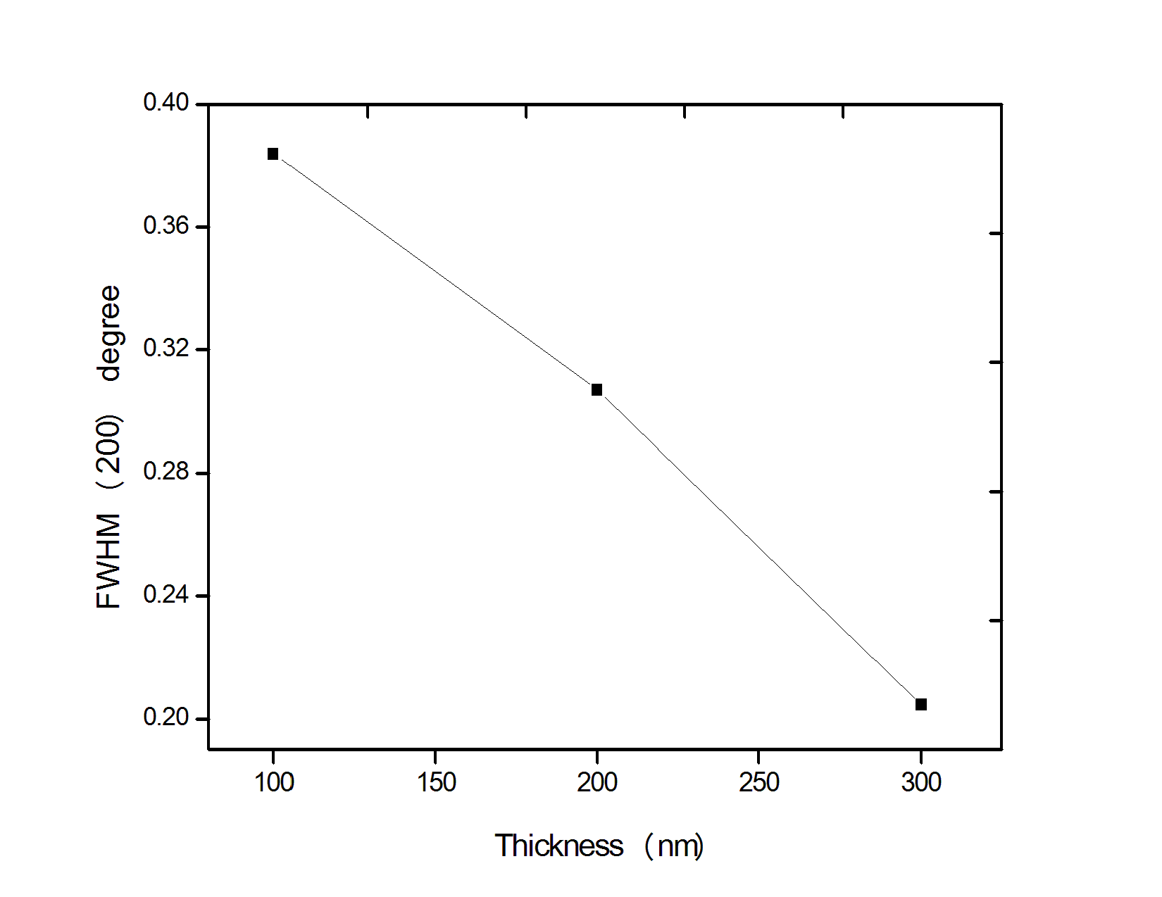
- A typical PbS solution procedure involves: 1. Thiourea solution [CS (NH2)2]: This solution was prepared with molarities (0.1M), from solving (0.761gm) of thiourea in (100ml) of distilled water and was marked solution 1.This solution was vigorously stirred using a magnetic stirrer about 10 minutes. 2. Lead Nitrate solution [Pb(CH3CO2)2· 3H2O]: This solution was prepared with molarities (0.1M), from solving (2.78gm) of lead acetate in (100ml) of distilled water and was marked Solution 2. This solution was vigorously stirred using a magnetic stirrer about 10 minutes. A solution 1 was added to solution 2 and vigorously stirred using a magnetic stirrer and was marked solution 3. PbS thin films were deposited from a solution 3 by chemical spray pyrolysis technique on glass substrate. In order to get uniform thin films, the height of the spraying nozzle and the rate of spray process were kept constant during the deposition process at 35 cm and 15 cm3/min. The spraying process lasted about 6 sec. The period between spraying processes was about 1 min; this period was enough to avoid excessive cooling of the substrate. PbS thin film was deposited on glass substrate at a temperature of 325℃ and a concentration of 0.1 M. The crystallographic structure of the PbS thin films deposited on the glass substrates was determined with a high resolution X-ray diffractometer system (Model: Panalytical Empyrean) with CuKα radiation (λ) of 0.154 nm. The surface morphology of PbS thin films was determined with Scanning Tunneling Microscope (STM) (Model: NT-MDT Solver Nano). The film thickness was measured by the gravimetric method. The electrical properties of PbS thin films was measured by Hall measurements (HL5500PC) system.
3. Results and Discussion
3.1. Structural Properties
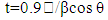
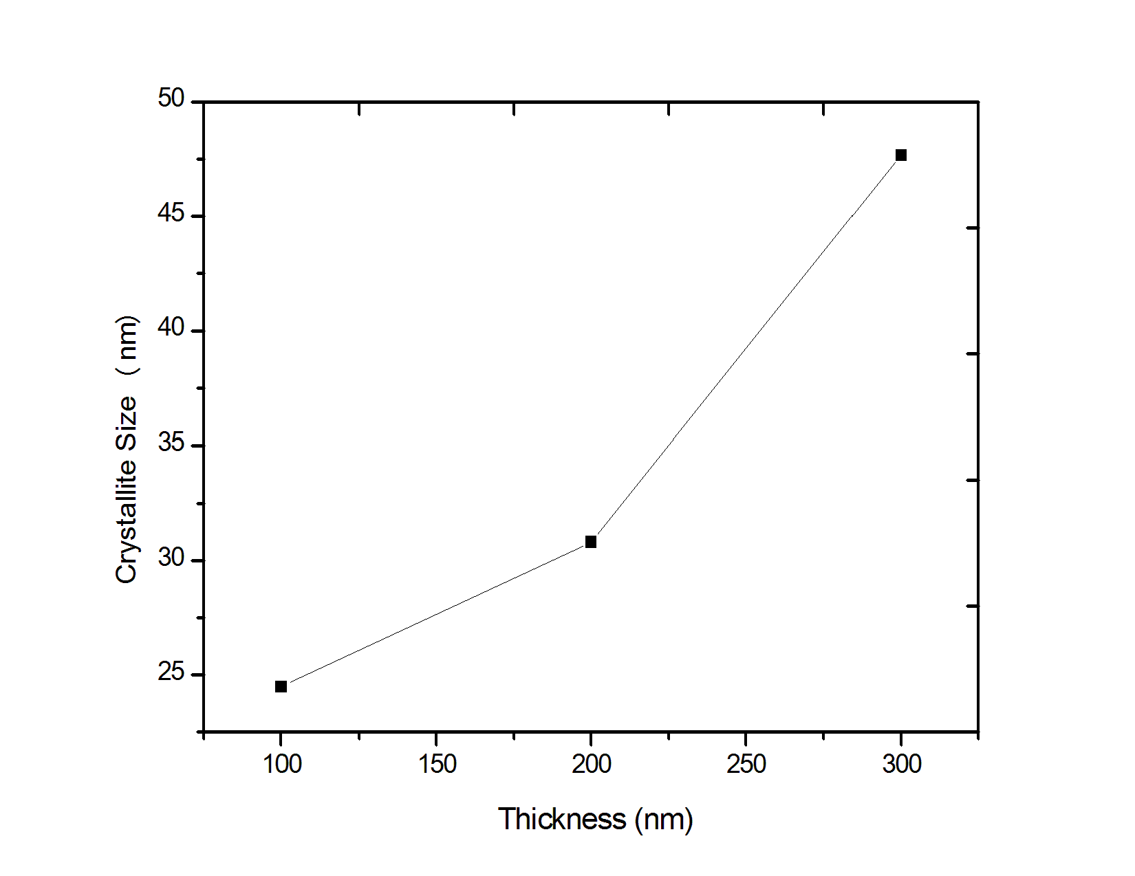
- The X-ray diffraction patterns of PbS films with different thickness are show in Fig. 1. All PbS films have cubic rock salt (NaCl) type structures. XRD patterns of all the PbS thin films showed sharp [1 1 1] and [2 0 0] peaks along with minor peaks of [2 2 0], [3 1 1], [2 2 2] and [4 0 0] planes to cubic structure of PbS thin films, as confirmed by standard ASTM card (No. 030660020). It has been observed that the intensity of the peaks increased and the crystallization of PbS thin films were improved with increasing film thickness, similar to other reports [12].For all films the preferential orientation value of [200] plane has the highest value compared to other planes. This result indicates a strong orientation growth along that plane. This behavior is in agreement with that reported in standard literature [4]. The crystalline grain size (t) of the PbS films was determined with the Scherrer formula [13].
 | (3.1) |
 | Figure 1. X-Ray diffraction patterns of PbS thin film of different thicknesses: (a) 100 nm, (b) 200 nm and (c) 300 nm |
 | Figure 2. Crystalline grain sizes as a function of thickness |
 | Figure 3. Variation of FWHM of (200) plane of PbS films with thickness |
 | Figure 4. STM analysis of PbS films deposited on glass substrates with different thicknesses |
 | Figure 5. Variation of the RMS roughness with different thicknesses |
3.2. Electrical Properties
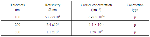
- Table 1 shows the dependence of the electrical resistivity and carrier concentration on the thickness films. The results indicate that PbS films exhibit p-type conductivity. The decrease in the resistivity of the PbS film with increasing the thickness. This behavior is in agreement with other reported [18, 19]. The carrier concentration of the films increases with the increasing film thickness. It can be explained with the fact that resistivity is known to be inversely proportional to the carrier concentration.
|
4. Conclusions
- Lead sulfide (PbS) thin films were deposited on glass substrates with chemical spray pyrolysis. The thickness of the films varied from 100 to 300 nm. Effects of thickness on the structural and electrical properties of the films deposited were studied. The characteristics of PbS thin films were investigated by various tools. X-ray diffraction patterns confirm the proper phase formation of the PbS. For all films the preferential orientation value of (200) plane has the highest value compared to other planes. The grain size of the PbS films increased with increasing thickness. The values of crystallite size were found to be in the range 24.49-47.66 nm. From STM images it was found that the root mean square roughness of film surface increased as the film thickness increased. From the electrical properties, it was found that PbS films with different thickness always show p-type conductivity.
ACKNOWLEDGEMENTS
- Author wishes to thank department of physics/ Faculty of Science and Health/ University of Koya/ Kurdistan Iraq.