-
Paper Information
- Paper Submission
-
Journal Information
- About This Journal
- Editorial Board
- Current Issue
- Archive
- Author Guidelines
- Contact Us
American Journal of Condensed Matter Physics
p-ISSN: 2163-1115 e-ISSN: 2163-1123
2015; 5(1): 1-9
doi:10.5923/j.ajcmp.20150501.01
Novel Approaches to Nanosensory Systems Development
 Abstract
 Reference
 Full-Text PDF
 Full-text HTML
P. J. Kervalishvili
Georgian Technical University, Tbilisi, Euro Mediterranean Academy of Arts and Sciences, Lausanne
Correspondence to: P. J. Kervalishvili, Georgian Technical University, Tbilisi, Euro Mediterranean Academy of Arts and Sciences, Lausanne.
| Email: |  |
Copyright © 2015 Scientific & Academic Publishing. All Rights Reserved.
Last achievements in physics and technology of nanostructured materials make possible to elaborate the nanosensors and their smart systems of different application based on quantum effects taking place in nanomaterials with semiconductor properties. The solution of this task is closely connecting with novel nanotechnology methods and tools for preparation of semiconductor nanosystems. Elaboration of quantum effects based devises very depends to micro and nanostructures properties. The hot atom clusters formed in the laser-plasma organized vapor are depositing on the substrate and performing in relevant structures of different sizes. At sub molecular level the physical effects are very sensitive to size of the film and its structural characteristics. Using this kind of nanostructured films it is possible to organize spintransport based processes and build up the quantum systems responsible for high effective sensory devices.
Keywords: Nanosensors, Devises, Nanostructured materials, Quantum effects, Structural characteristics, Semiconductor properties
Cite this paper: P. J. Kervalishvili, Novel Approaches to Nanosensory Systems Development, American Journal of Condensed Matter Physics, Vol. 5 No. 1, 2015, pp. 1-9. doi: 10.5923/j.ajcmp.20150501.01.
Article Outline
1. Introduction
- Concern over the consequences of harsh environmental pollution, particularly in nuclear power engineering and military base sites rise to an increasing demand for suitable means of monitoring a number of radioactive sources enriched gases, vapors at and around the occupational exposure limits. For instance, radioactive pollutants generated directly or indirectly, as a result of nuclear waste influence on different substances working in nuclear power stations (water, gases, metals, etc.) or existing nearby radioactive materials places.The need is for devices that can achieve the necessary sensitivity at a cost that will not prohibit their widespread deployment and with the capabilities to provide quantitative information as well as alarm functions.These devices and particularly detectors of nuclear radiation with autonomous energy supply are very useful for illumination and prevention of nuclear materials illegal transportation and transfer. The development of new range of sensors has provided instruments with enhanced selectivity and sensitivity for harsh, radioactive waste polluted environment monitoring [1].Development of effective sensors and sensory systems (networks) united in artificial intelligence grid is also very important for Black Sea and Mediterranean basin areas, where are some rather problematic territories in point of view of different radiation waste: Martkophi and Matkhoji-Udzluuri sites in Georgia, Artik and Metsamor in Armenia, Kozloduj in Bulgaria and others. During the Cold War era, there were two major competitive research groups making gamma and neutron radiation detectors (sensors): Lawrence Berkeley National Laboratory Semiconductor Detector Group and the USSR’s Middle Machinery Ministry (comprising Kurchatov Institute of Atomic Energy, Giredmet Institute of Rare Metals, Institute of Radioisotope Devices, etc). Both competitors were focused on the development of semiconductor-based radiation detectors and their applications. The best sensor material for gamma radiation sensors was, and still is, ultra pure Ge and Si or Ge doped by Ga impurities with acceptor concentration up to 1016 cm-3. For neutron radiation measurement the B isotopes contained Si was developed [2]. Determination of appropriateness and mechanisms of the influence of the isotope effects on the properties of the medium opened new possibilities to pass from the technology of isotope substances pure in the sense of admixtures to the technology of pure isotope substances. Purposeful usage of isotope effects in certain physical phenomena and processes will substantially extend the sphere of utilization and production of stable and unstable isotopes [3].Such approach to isotope problem leads us to perspective branches of physics and technology – physics and isotope stimulated phenomena and isotope material science. This relatively new field of solid state physics as well as of molecular physics includes the study of isotope effects of various media. Isotope effect is very effective for nuclear radiation sensors preparation. Today, nuclear radiation detection systems exist utilising a variety of solid state detectors. The solid state detectors are based on semiconductor material such as silicon, germanium, cadmium telluride, zinc oxide, etc. A major advantage of such detection systems is their extremely high energy resolution. Another prospective application of isotope effects is their utilisation in quantum spin based devices. In the last years the strong attention was paid to development of so called “high temperature boron and its compounds because of their suitable physical and chemical features as the sensitive elements for temperature and nuclear radiation sensors. They are semiconductor materials (mainly boron and boron carbide) with a high melting point, mechanical/ chemical strength in corrosive media and strong atomic bonds providing high stability in the radiation area. To raise its radiation resistance under neutron irradiation, boron should be enriched with 11B isotope. In case of semiconductor Boron based elements preparation enriched by 10B following n, α nuclear reaction it is possible to build a very sensitive neutron detectors [4].Last achievements in nanoscience and nanotechnology lifted the effectiveness of semiconductor sensory devices on the higher level. It had been arisen possibilities of creation of nano and micro size radiation sensors and sensory systems as well as their networks. Novel achievements well indicate that micro – and nano – worlds are continuously merging. In some cases “nano” products emanate as natural, inevitable extensions of their well established “micro” precursors simply by the downscaling of conventional technology. Following that in the nearest future the similar extension should be elaborated for the “pico” matter, and as result – to picotechnology [5].In general there are two fundamental approaches for the new nano materials and devices realization: In a top down approach structures are miniaturized mainly by means of well established metal powders or semiconductor structures and instruments fabrication technologies; In a bottom up approach materials as well as functional systems are made by assembling of nanosized components like carbon nanotubes or DNA. There are several brilliant phenomena associated with micro – nano size materials and devices. At the same time it is necessary to take into account and find the limit of the miniaturization of micro – and nano – structures. It is very important to identify the classes of condensed matter substances and systems that are better suited to micro – nano world, where they will operate most effectively.Nowadays, due to issues of nuclear non-proliferation and international security, new and much stricter requirements for nuclear radiation sensors and sensory systems have been created. The issue of developing novel sensors compliant with the new requirements poses interesting technical challenges for researchers and engineers. The new sensors need to rely on one or more sensing mechanisms and produce a signal that indicates the nuclear/ionizing radiation value. It is also necessary to operate by so called smart or intelligent sensor systems, in order to have precise measurement information about nuclear/ionizing radiation.Nano micro sensor systems integrate and interface multiple core technologies and related devices to implement a variety of functions. They can be implemented through scalable homogeneous, or heterogeneous hardware integration technologies, in order to advance the miniaturisation, functionality and reliability of the sensor, processor, actuator and communication functions. Power autonomy (consumption and supply) is a common issue. In the medium term, there is growing industrial interest to integrate nanosensors in smart (intelligent) microsystems, mainly due to an increase in sensitivity, device simplification and associated cost reduction. The development bubble chart represents the range of sensors and sensory systems capabilities and activities and covers the span from underlying science to the engineering developments required to deliver devices, instruments, and systems. At the same time, the existence of integrated technologies facilitates the transfer of information for improvement of appropriate sensing mechanisms and devices (Fig.1), [6].
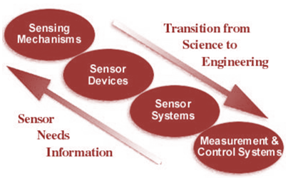 | Figure 1. Sensor Technolog Overview |
2. Boron Isotopes Based Semiconductor Nanosensors
- Last decades our research group started the work to develop novel boron-based nanosensory elements for temperature and neutron sensors that can operate in harsh environments (corrosive media, nuclear radiation, etc.) Boron is a wide-range high temperature semiconductor with a prohibited energy zone of about 1,6 eV. Boron carbide (B4C) and some other boron rich compounds have a similar forbidden energy gap, which defines their electrical resistance. High mechanical and chemical strength in various corrosive media, and the possibility to change the isotope content from 11B to 10B in almost every concentration range, allows to improve the radiation resistance of boron based sensors and nanosystems. Boron (and its compounds) crystalline and compact pellets are possible to be prepared by different metallurgical methods: vacuum synthesis, melting zone, free crystallization, vacuum hot pressing, sintering hot compaction, self-propagation high-temperature synthesis, gasostatic pressing, etc. Study of their properties such as the temperature resistance, voltage-current characteristics, ice melting point sensitive response, structural stability, etc. showed a high temperature resistance coefficient and linearity of voltage-current parameters within their operational range. Using such approaches researchers have managed to produce compact pellets made of boron, boron carbide and aluminium dodecaboride etc. Typically, the pellets had a cylindrical or thick disk shape, high density, low concentration of metallic impurities, and room temperature electrical resistance in the range 106 - 108 Ohm.m. One more advantage of boron and its compounds is the preparation of sensitive elements in types of ceramic thin films, nanostructured elements, quantum dots and other nanosystems, which make possible to obtain different properties materials and sensitive elements [7-9].Temperature dependence of boron, boron carbide and aluminum dodecaboride electric resistance was studied in 150-750 K temperature range. A thermostat provided the temperature constancy by the following transient phases: melting, boiling and eutectics solidification. The points corresponding to the eutectic solidification temperatures were obtained using aqueous solutions of the eutectic composition, which form cryohydrates coinciding with the liquid phase by their composition. A Chromel-Alumel thermocouple and a platinum resistance-thermometer measured the temperature at the constant point. The electric parameters of the sensitive elements were measured with a measuring bridge circuit. The example of temperature dependence of the resistance of the aluminum dodecaboride enriched by 11B is shown at the fig.2.
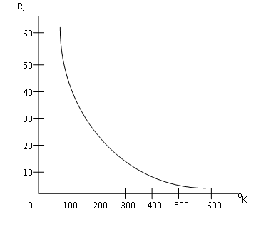 | Figure 2. Temperature dependence of the electroresistance of AlB12 enriched by isotope  |
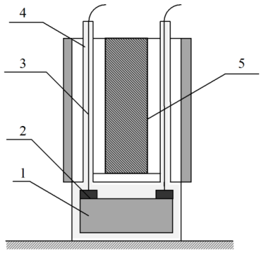 | Figure 3.  enriched B4C sensory element based temperature microsensor: 1) Disk-shaped plate containing boron; 2) Nickel ohmic contacts; 3) Electrodes; 4) Chemically resistant lacquer (to protect sensor element, contacts and electrodes from moisture and corrosive medium effects); 5) Sensory element enriched B4C sensory element based temperature microsensor: 1) Disk-shaped plate containing boron; 2) Nickel ohmic contacts; 3) Electrodes; 4) Chemically resistant lacquer (to protect sensor element, contacts and electrodes from moisture and corrosive medium effects); 5) Sensory element |
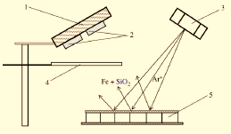
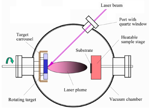 | Figure 4. Laser Plasma Deposition Process |
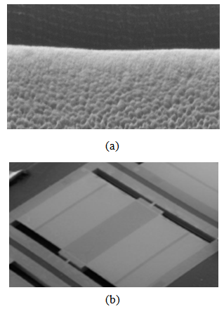 | Figure 5. Novel boron-based nanosensor: a – surface; b – element |
3. Quantum Effects in Nanostructures and Nanosensors
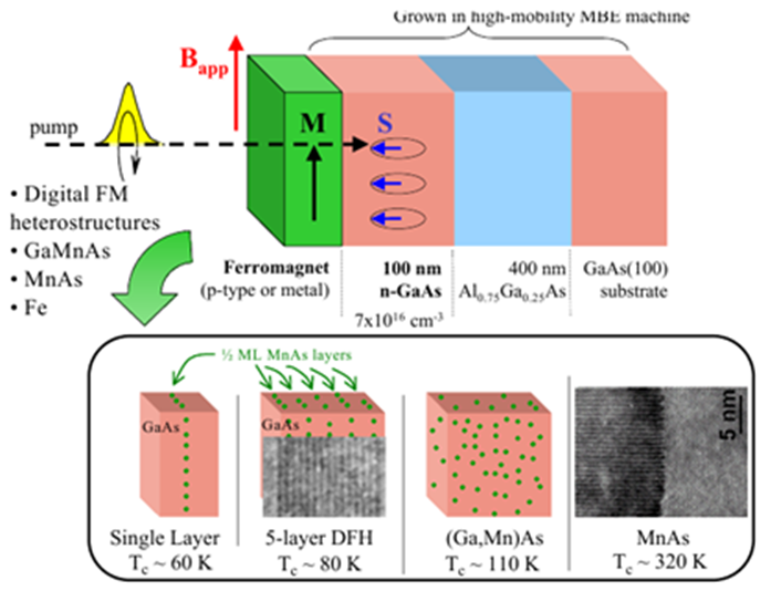
- Radiation sensors are systems that act as interfaces between incident radiation and imaging systems. The most effective way for organization of information transfer in these kind of systems is quantum effects utilization.Recent study of the spin transfer in semiconductor nanosystems enriched by ferromagnetic dopants have determined the most essential mechanisms, responsible for spin transport properties, best solutions for electronic and magnetic structures preparation and for the development of technologies of spintronic materials with controlled disorders. Elaboration of precise methods of semiconductor nanostructures and systems preparation is extremely necessary for combination of well controlled spin electronic properties for semiconductors with additional possibilities of devices with the spin degree of freedom of current carriers. For this kind of quantum nanosensors it is the central problem today the search of an effective way for the spin injection in a semiconductor sensory element from the spin-polarized reservoir [17, 18]. Generally quantum sensors are devices those exploit quantum correlations to achieve a sensitivity or resolution that is better than can achieved using only classical systems can measure the effect of the quantum state of another system on it. The sensors operating with the tunnel magnetic junctions (MTJ) are the good example of spintronic quantum devices. There ferromagnetic electrodes are divided by very thin dielectric layer, and electrons are tunneling through a nonconducting barrier under influence of applied voltage [19].Possibility of development of these sensory devices is connecting nowadays with the creation of spin transistors. In this case spintronic devices may not only switch or to detect electrical and optical signals, but also to enhance them, and to be used as multifunction units. Only in this case spintronic devices can not only switch or detect electrical and optical signals, but to enhance them and can be used as multifunction units. Nanospinelectronics, based on usage of magnetic materials, represents new area of science and engineering. The reason to that is the perspective of creation of principally new devices for information technologies operating as charge, and spin degree of freedom of carriers, free from limitations inherent for metal spinelectronic devices. The main structural property of materials in which we can observe novel nano dimension phenomena is their unperfection – high concentration of different defects connected with several impurities of metal and non metal chemical elements. So, novel very exiting properties of semiconductors are determined by impurities and their disordered distribution. At the same time the last theoretical and experimental achievements have shown that disorders in semiconductors should be controlled – should have a necessary rules and regulations [20]. By these approaches it is possible to define the link between matter and information which is most evidently manifested by the molecular constitution in building molecules connecting in given order. The initial formation directs the synthesis of sequences, which logically are not random; there is an optimization of structure within the system. Such optimization should be expressed in terms of fuzzy entropy and it relates directly to the definition of information. Following novel achievements we could integrate the science and technology of small scale structures (nano, pico structures [6]), quantum size elements based physical effects and information-communication processes, which brings us to novel applied science discipline – quantum information technology (QIT) [21]. All approaches treat the nonmagnetic and ferromagnetic metals as free electron materials. Based on the assumption that the elastic scattering time and the inter band scattering times are shorter than the spin flip times the two current model is adequate to describe and explain the observed magnetoresistance effect. However, it is unable to quantify the bulk and interface spin asymmetry parameters and spin relaxation lengths As since Magnetism originates from the spin of the electron, having a much larger magnetic moment than the nucleus of an atom. A net electron spin in an atom results from flexibility of ordering in the electronic arrangement of the electrons around the nucleus and the requirement for the electron wave function to obey the Pauli exclusion principle, that is: the complete wave function of a two or more electron system has to be antisymmetric with respect to the interchange of any two electrons. Therefore the symmetry (symmetric or antisymmetric) of the spin part of the wave function influences the symmetry of the spatial wave function and hence influences the total Coulomb energy of the electron system. The difference in energy between a two electron system with a symmetric (triplet) or antisymmetric (singlet) spin part of the wave function is referred to as the exchange energy. For example, ferromagnetism exists in some elements due the dependence of the Coulomb energy (the exchange energy) on the particular arrangement of the electrons and their spin in the 3d shell. The concept of spin injection and accumulation is based on induced magnetization in a nonmagnetic metal. However one this description of spin injection and accumulation is only valid in the situation where a nonmagnetic metal is weakly coupled via tunnel barriers, to its electrical environment [22]. So-called magnetic discrete alloys todays are of the most prospective materials for solution of the spin injection problem. These alloys involve a periodic system of sub-monolayers of magnetic ions (for example, Mn), placed between semiconducting layers (GaAs, GaSb, InAs) forming a magnetic superlattice. There are as incidentally distributed Mn ions and 2d magnetic islands of MnAs (or MnSb) as well in manganese containing layers. The discrete alloys have high Curie temperatures (above 300 K for the GaSb-system), demonstrate extraordinary Hall Effect at high temperatures and have a relatively high degree of the spin polarization. It is possible in such systems to control not only quality of the border "ferromagnetic metal - non-magnetic semiconductor", but also manage of the current carrier’s concentration and change the type of magnetic ordering. The discrete alloys should be considered as random magnet systems owing to hardly inhomogeneous allocation of a magnetic phase in sub-monolayers [23]. Operation of a spintronic device requires efficient spin injection into a semiconductor, spin manipulation, control and transport, and spin detection. The relevant role in solution of this problem is shunted to search and investigations of new ferromagnetic materials, which are capable to be reliable and good spin injectors. Among such objects the magnetic discrete alloys are very promising. They are multilayer systems composed of submonolayers of a ferromagnetic material in the matrix of a non-magnetic semiconductor, for example, Mn/GaAs or Mn/GaSb. It is well known, that these alloys have high Curie temperatures and sufficiently high spin polarization. The circumstance is not less important that it is possible to control and to manage of the "ferromagnetic metal - semiconductor" boundary surface immediately during the synthesis of these materials. As it was investigated recently they should be prepared by the methods of the MOS hydride epitaxy Ion beam sputtering (fig. 6) and mostly by laser epitaxy with usage of pulsed annealing of epitaxial layers [24, 25].
 | Figure 6. The scheme of the setup for composite film deposition by ion-beamsputtering of the compound target: (1) substrate holder with heater, (2) substrate, (3) ion-beam source, (4) shutter and (5) target |
 | Figure 7. Electron Spin Coherence in Ferromagnet/GaAs Nanostructures [26] |
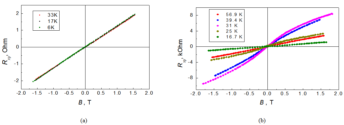 | Figure 8. Hall effect in quantum-sized GaAs(δ-Mn)/InхGa1-хAs/GaAs structures with metallic (a) and activation (b) type of conductivity at different temperatures [31] |
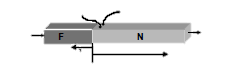 | Figure 9. Schematic representation of the experimental layout for electrical spin injection: with λF and λN on either side of the F/N interface represent the distance where the spin accumulation exists in the F and N metal |
4. Conclusions
- The unique properties of well known semiconductors: Germanium, Silicon, metal oxides, etc. are reachable by precise doping of different impurities (Boron isotopes, 3d metals, etc.) makes possible to establish of different high sensitive devices, and among them gamma and neutron radiation sensors of high resolution; temperature sensors working in harsh environment; resistive nanosensors with memory, and others [33, 34]. These smart instruments should be integrated in recently developing intelligence networks including quantum information technologies based ones, which determine their high sensory characteristics and possibility of precise management and control in wide spectrum of applications. It should be taken into account that in various conditions it is a very convenient to use the semiconductor boron and its main compounds as the sensitive elements for different types of radiation sensors as well as for sensory systems working in critical sites and harsh environment. The Boron and refractory borides which are high temperature and high resistance wide forbidden zone semiconductors and their physical properties including the variation of isotope concentration are very prospective for application in aggressive media where they are stable working elements for a long time. Besides of it they are very attractive for future developments of micro and nanosystems as the multiapplicable semiconductor elements. Above mentioned materials based sensors and sensory systemsas well as quantum effects based nanostructured magnetic solid state ones open the new ways for preparing the novel radiation sensorydevices with unique characteristics.
ACKNOWLEDGMENTS
- The paper was prepared in the framework of EU FP7 SENSERA project.