N. E. Makori, I. A. Amatalo, P. M. Karimi, W. K. Njoroge
Department of Physics, Kenyatta University, Nairobi, Kenya
Correspondence to: N. E. Makori, Department of Physics, Kenyatta University, Nairobi, Kenya.
| Email: |  |
Copyright © 2014 Scientific & Academic Publishing. All Rights Reserved.
Abstract
Tin Selenide (SnSe) thin films were optimised for thin film solar cell applications. The thin films were successfully deposited by thermal evaporation using Edward’s Auto 306 Magnetron Sputtering System. Their optical and electrical properties were studied using Solid Spec-3700 DUV Spectrophotometer and Four Point Probe method respectively. The deposited SnSe thin films had transmittance ranging between 1- 45%. SCOUT 98 Software was used to obtain optical band gap values and absorption coefficients of SnSe thin films. Optical band gap values obtained were in the range of 1.71-1.76eV. The thin films showed decrease of resistivity from 181-120Ωcm with increase in film thickness from 112-148 nm. Low transmittance of SnSe implies high absorption coefficient which is one of the important parameter to be considered when choosing absorber layers for thin film solar cell applications.
Keywords:
Thermal evaporation, Thin film thickness, Optical properties, Electrical properties
Cite this paper: N. E. Makori, I. A. Amatalo, P. M. Karimi, W. K. Njoroge, Optical and Electrical Properties of SnSe Thin Films for Solar Cell Applications, American Journal of Condensed Matter Physics, Vol. 4 No. 5, 2014, pp. 87-90. doi: 10.5923/j.ajcmp.20140405.01.
1. Introduction
Energy consumption has increased steadily with civilization. Energy crisis due to a decline in fossil fuel stocks and increasing carbon dioxide emissions that are causing global warming has enhanced interest in the development of clean renewable sources of energy. To sustain human development, more electrical energy consumption is expected in future [1]. Solar cells hold great hopes for use as an environmental friendly and economically viable renewable source of energy.Recently, the search for thin-film materials for solar energy conversion and other related applications has been intensified with SnSe as one of the absorber materials. The solar cell industry is predominantly using Silicon based solar cell technology. Because of its indirect band gap silicon is not able to absorb much sunlight as compared to direct band gap materials [2]. Due to its low absorbability, thicker silicon layers are required to absorb the same amount of light as any thin layer of direct band gap material. This has necessitated research on thin film solar cells which use less inexpensive material. A Lot of effort has been geared towards metal chalcogenides as they have shown superior performance as compared to others [3]. Metal chalcogenides have been prepared in form of thin films by various researchers. For large scale production of solar cells, a thin film deposition technique that can be easily handled at low cost is needed [4].Tin Selenide is a narrow band gap binary IV-VI semiconductor material. It is thus capable of absorbing a major portion of solar energy hence its use in fabricating solar cells. It is also suitable for various optoelectronic applications like memory switching devices, light emitting devices (LED), holographic recording systems among others. Optical and electrical properties of SnSe thin films are dependent on the preparation technique. Thermal evaporation is the most commonly employed method in preparation of thin films because it is very simple, economical, and convenient [5]. The electrical data of SnSe shows that the thin films are semi-conducting in behaviour with p-type conductivity. The existence of tightly bound double layers of tin and selenium atoms stacked along the crystallographic c-axis of SnSe structure, suggests the bonding between the layers being weak van der waals type, which leads to a highly pronounced layered type of structure. Such a structural arrangement of SnSe leads to a pronounced anisotropy of its physical properties, which makes it particularly appealing for the fabrication of solar cells as it has a narrow optical energy band gap implying high optical absorption in the visible region of the electromagnetic spectrum. Moreover, SnSe has higher chemical stability without passivity as compared to other semiconductors, such as Si, InP, GaAs and CdSe, which need special passivity procedures in order to avoid photocorrosion [6]. Tin based solar cells exhibit good optical properties and its alloys have high efficiency solar cell materials [7]. Optical band gaps of SnSe2 and SnSe prepared by heating are 1.27eV and 1.03 eV respectively [8]. The films are efficient in the solar cells for an optical band gap of 1-2.7eV and electrical conductivity of 0.01-0.25(Ωcm)-1. Tin Selenide has drift mobility for holes as 0.7m2(Vs)-1 [9]. Fabrication and characterization of polycrystalline thin film of SnSe done by [10] using vacuum deposition at a substrate temperature of 423K the films were photosensitive. The photosensitivity was found to increase with illumination of the thin films. The influence of substrate temperature on the growth of SnSe thin films prepared by evaporation by [11] at a substrate temperature of 513K, had a direct band gap of 1.26eV with high absorption coefficient >104cm-1 near the fundamental absorption edge. The films were found to be p-type. The electrical resistivity varied from 3.0-8.1Ωcm in the thickness range of 150-300nm.
2. Experimental Procedure
Thermal evaporation of SnSe thin films was done in Edwards Auto 306 Magnetron Sputtering System. Tin and selenium elements were mixed in a ratio of 1:1 and heated in a glass tube until they melted to form a homogeneous alloy. The alloy was allowed to cool in sealed glass tube to prevent oxidation of Tin and Selenium. Clean glass substrates were then mounted on a substrate holder of the Edwards Auto 306 Magnetron Sputtering System. Five samples of mass 1.00g, 1.05g, 1.10g, 1.15g and 1.20g of the alloy were each placed on a boat and then the chamber covered tightly and chamber evacuated to a base pressure of 3.2 x 10⁻⁵ mbars. A constant current of 3.2 A was supplied to the heater to evaporate the samples to form SnSe thin films of varying thickness. The deposition time was 1 minute and was maintained for all SnSe thin films. Substrate to boat distance was maintained at 15.0 cm throughout the whole thin film deposition process. Film thickness of SnSe samples was determined using a Profilometer. | Table 1. Deposition parameters of SnSe thin films |
| | Parameter | Units | | Deposition Temperature | 448 K | | Base Pressure | 3.2 x 10⁻⁵ mbars | | Heater Current | 3.2 A | | Substrate to Boat Distance | 15.0 cm |
|
|
3. Results and Discussions
3.1. Transmittance of SnSe
The optical transmittance spectra were obtained in the 300nm-1000nm wavelength range by using a Solid Spec 3700 DUV Spectrophotometer. Transmittance of the SnSe thin films deposited varied with film thickness. A transmittance of 0.01- 45% for photons of wavelength between 300-1000 nm was obtained. SnSe thin films of thickness 112 nm had the highest transmittance between 1 - 45% while SnSe of thickness 148 nm had the lowest transmittance of 1-35% for photons of wavelength between 300-1000 nm as shown in figure 1. This is because as the film thickness increases, the strain value decreases because of the influence of the glass-SnSe lattice mismatch implied generation of defects in the SnSe layer close to the glass substrate. These defects gradually decrease as the film thickness increases. The transmission spectra of SnSe are shown in figure 1.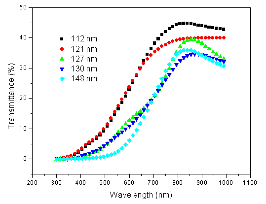 | Figure 1. Transmittance spectra of SnSe thin film samples |
3.2. Absorption Coefficient of SnSe Thin Films
It was observed that, SnSe thin films of thickness 148 nm had the highest absorption coefficient while thin films with a thickness of 112 nm had the least absorption coefficient as shown in figure 2. This is because of reduction in stacking faults and lattice defects as film thickness increased; thus an improvement in film crystallinity [12]. High absorption coefficient is achieved when the photon energy is higher than the energy gaps of a semiconductor material.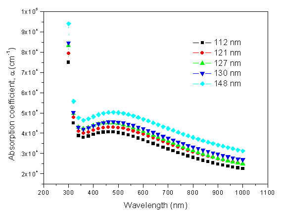 | Figure 2. Variation of absorption coefficient with wavelength |
3.3. Energy Band Gap of SnSe
Energy band gap of SnSe was extracted from the simulated transmittance data of SCOUT 2.4 software. The band-gap energy and the transition type can also be derived from the mathematical treatment of the data obtained from the optical absorbance versus wavelength using equation 1. | (1) |
The optical energy band gap decreased with increase in film thickness from 112 nm to 148 nm as shown in figure 3. 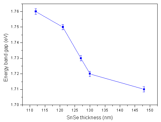 | Figure 3. Variation of Energy Band gap with Film thickness |
The decrease in the optical energy band gap with increase in film thickness from 112 nm to 148 nm may be attributed to the fact that the density of localized state in the films increases with film thickness which leads to decrease in the band gap. The energy band gap of SnSe samples prepared ranged between 1.71-1.76 eV.It is assumed that the absorption coefficient (α), in equation (1) near the band edge shows an exponential dependence on photon energy for many materials [13]. This dependence is given as follows in equation 2.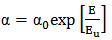 | (2) |
Where, αo, is a constant and Eu is Urbach energy which is the width of the tail of the localized state associated with the amorphous state in the forbidden band.The slight difference in band gap values from those reported in other studies can be attributed to variation of deposition conditions and film thickness. The variation of absorption spectra with optical energy band gap is shown in figure 4.  | Figure 4. Absorption spectra of SnSe thin films samples |
Tin Selenide thin films of thickness 148 nm had the highest absorption while that of thickness 112 nm had the least.
4. Electrical Resistivity of SnSe
Sheet resistance measurements of SnSe were done using Four Point Probe method. The sheet resistance obtained were used to calculate resistivity of SnSe thin films using equation 3. | (3) |
 = 4.53, In typical usage the current is set to 4.53 mA so that the resistivity is simply the voltage reading in mV.Figure 5 and table 2 show the variation of resistivity with SnSe thickness. Resistivity of SnSe decreased with increase in film thickness.
 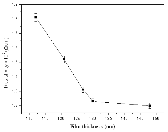 | Figure 5. Resistivity of SnSe with film thickness |
| Table 2. Electrical Properties of SnSe Thin Films |
| | Film thickness ± 2 (nm) | Sheet resistance x 106 ± 500 Ω/υ | Resistivity x 102 Ωcm | | 112 | 3.56 | 1.81 | | 121 | 2.77 | 1.52 | | 127 | 2.27 | 1.31 | | 130 | 2.09 | 1.23 | | 148 | 1.79 | 1.20 |
|
|
The SnSe thin films were showing decrease in resistivity from 181-120 Ωcm with increase in film thickness as shown in figure 5 and table 2. This can be explained using Petritz barrier model. According to the model, the crystallites do not grow sufficiently large at low energy or temperature and the larger inter-crystalline regions offer high resistance for the movement of charge carriers. At high substrate temperature or energy, the formation of fewer nucleation centre results in large crystallite size, which decreases the inter-crystalline barriers, hence decrease in electrical resistivity. Similar resistivity measurements were reported by [14] where resistivity ranged between 112-20 Ωcm at different substrate temperatures.
5. Conclusions
Tin Selenide (SnSe) thin films were successfully deposited on glass substrate using thermal evaporation method. The thin films prepared had an optical transmittance of range between 0.01- 45% within the visible light region. The optical energy band gap decreased from 1.76 - 1.71 eV with increase in film thickness from 112 nm to 148 nm. The thin films were showing decrease in resistivity from 181-120 Ωcm with increase in film thickness from 112-148 nm. High absorption coefficients and low transmittance of SnSe thin films indicates that SnSe is appropriate for use as absorber layer in thin film solar cells. Of the five samples prepared, SnSe thin film of thickness 148 nm is the most appropriate for use in thin film solar cell applications because of its high absorption coefficients and relatively low electrical resistance as compared to other samples.
ACKNOWLEDGEMENTS
We extend our heartfelt thanks to the laboratory technicians of Physics Department Kenyatta University under the guidance of the Chief Technician Mr. Simon Njuguna particularly in their technical input in the maintenance of the Edwards magnetron Sputtering System. Our special thanks also go to Mr. Boniface Muthoka; technician Physics Department University of Nairobi-Chiromo Campus for his technical input in the use of the Solid Spec 3700 DUV Spectrophotometer.
References
| [1] | Kuo-Jui, H., 2010. Electron-Reflector strategy for CdTe thin-film solar cells. PhD Thesis. Colorado State University, Department of Physics, USA. |
| [2] | Fahrenbruch, A. L. and Bube R .H., 1983. Fundamentals of solar cells. New York Academic Press, USA. |
| [3] | Lindgren, T., Larsson M. and Lindquist S., 2002. Solar energy materials. Journal of Solar cells, 73, 377-377. |
| [4] | Mariappan, R., Ragavenda M. and Gowrisankar G., 2010. Growth and characterization of SnSe thin films prepared by spray pyrolysis technique. Chalcogenide Letters, 7, 211- 216. |
| [5] | Kumar, N., 2012. Effect of film thickness on optical properties of tin selenide thin films prepared by thermal evaporation for photovoltaic applications. American Journal of Materials Science, 2, 41- 45. |
| [6] | Aruchamy, A., 1992. Photoelectrochemistry and photovoltaics of layered semiconductor. Kluwer Academic Publishers, Dordrecht. |
| [7] | Toshiyuki, Y., Jiro M. and Akira Y., 1991. Thin films of CuInSe2 prepared by RF sputtering from various compositional powder targets. Solar Energy Materials and Solar Cells, 27, 25-35. |
| [8] | Bindu, K. and Nair P., 2004. Semiconductor tin selenide thin films prepared by heating Se-Sn. Semiconductor Science Technology, 19, 1348-1353. |
| [9] | Madelung, O., 1992. Electrical characterization of tin selenide. Journal of Data in Science and Technology, 44, 122-127. |
| [10] | Pathinettam, P.D., Marikani A. and Murali K.R., 2000. Crystal Research Technology. Material Science, 35, 949-949. |
| [11] | Hema G., Naveen J. and Uthanna S., 2007. Preparation and characterization of flash evaporated tin selenide thin films. Journal of Crystal Growth, 306, 68-74. |
| [12] | Venkatachalam S., Mangalaraj D. Narayandass S., Velumani S., Schabes-Rechkiman P. and Ascencio J. (2007). Structural studies on ZnSe/p-Si schottky diodes. Material Chemistry and Physics, 103, 305-311. |
| [13] | Urbach, F., 1953. The long-wavelength edge of photographic sensitivity and of the electronic absorption of solids. Physical Review, 92, 1324-1324. |
| [14] | Kumar N., 2010. Influence of the substrate temperature on the structural, optical and electrical properties of tin selenide thin films deposited by thermal evaporation method. Crystal Research Technology, 45, 53-58. |
 Abstract
 Reference
 Full-Text PDF
 Full-text HTML