Ehssan H. Sabbar1, Mustafa H. Saleh1, Salih Mohammed Salih1, Sufian H. Salih2
1Renewable Energy Research Center, University of Anbar, Anbar, 31001, Iraq
2Computer and Information Technology Center, University of Anbar, Anbar, 31001, Iraq
Correspondence to: Mustafa H. Saleh, Renewable Energy Research Center, University of Anbar, Anbar, 31001, Iraq.
| Email: |  |
Copyright © 2012 Scientific & Academic Publishing. All Rights Reserved.
Abstract
In this paper, deposition of SeTe/Si as a thin film is used to fabricate solar cells. SeTe thin films with varying thicknesses (300, 600, and 750 nm) were deposited by thermal evaporation onto n-Si wafers at room temperature and under a vacuum pressure of 10-5 mbar. The films were then annealed at temperatures of 323 and 348 K. The current–voltage characteristics of the forward and reverse bias of the SeTe/n-Si heterojunction were determined to achieve photovoltaic efficiencies ranging from 0.8 to 4.1. The study results showed that the efficiency of the resulting heterojunction increases with increasing annealing temperature and thickness of the SeTe film.
Keywords:
SeTe/Si Deposition, Solar Cell Characterization, Heterojunction, Temperature
Cite this paper: Ehssan H. Sabbar, Mustafa H. Saleh, Salih Mohammed Salih, Sufian H. Salih, Deposition of SeTe/Si Thin Film via Thermal Evaporation, American Journal of Condensed Matter Physics, Vol. 3 No. 5, 2013, pp. 119-122. doi: 10.5923/j.ajcmp.20130305.01.
1. Introduction
Type IV–VI semiconductors are regarded as promising materials for optoelectronic applications. The applications of IV–VI layers (chalcogenides) on Si substrates in the mid-infrared region as optoelectronic emitters, sensors, and detectors have been discussed in[1–3]. Thin-film solar cells have the advantage of requiring only small amounts of active materials, which translates to a considerable reduction in material costs[4]. The high-quality epitaxial growth of SeTe and related materials on oriented Si (111) substrates has recently been achieved by incorporation of thin intermediate BaF2/CaF2 layers[1, 2]. Hetero-epitaxial growth of SeTe on silicon utilizes silicon integration technology to fabricate inexpensive photonic devices. SeTe layers grown heteroepitaxially on Si (111) have been fabricated and separated using a junction with a built-in field[5]. Once separated, the SeTe layers become majority carriers on either side of the junction. This excess majority carrier concentration is responsible for generating a voltage across the external circuit. When a load is attached to this circuit, the current may begin to flow. Electrochemical deposition of PbSe and CdTe nanoparticles onto p-Si(100) wafers and into nanopores in SiO2 layers grown thermally on p-Si(100) substrates (SiO2/Si(100) structure) under illumination were studied in detail in[6]. In this work, the authors used SiO2 layers with track to produce nanopores that were further developed by irradiation with Au ions at 350 MeV. The pore structure was formed by chemical etching of the irradiated SiO2 layer with dilute HF and shaped as truncated cones with base diameters ranging from 200 nm and 250 nm and a height of 200 nm. In[7], ZnO thin film diodes were fabricated by deposition of a Zn3P2 thin film on an n-type ZnO thin film followed by Nd:YAG laser annealing. A p–n junction was formed, and conventional diode characteristics were observed by current–voltage (I–V) measurement. ZnO thin film diodes were further fabricated by laser annealing of the Zn3P2/ZnO film. The results of this study showed that laser annealing to form ZnO p–n junctions allows efficient fabrication of ultraviolet ZnO light-emitting diodes and ZnO wide band gap diodes.The authors in[8] investigated ternary compounds of Ag2SeTe semiconducting thin films in detail. In this study, synthesis of thin films with varying thicknesses onto glass substrates at room temperature using thermal evaporation and a chemically synthesized target material was pursued. Analysis of the transmission spectra of Ag2SeTe films recorded from 400 nm to 1200 nm revealed that the optical absorption coefficient and energy band gap of films deposited at different substrate temperatures were 106 cm-1 and 1.48–1.59 eV, respectively. The direct optical band gap of the Ag2SeTe thin films deposited on glass substrates with various thicknesses (50–230 nm) ranged from 1.48 eV to 1.59 eV. The structural and optical parameters of the films were also found to be very sensitive to their thickness.In the current study, we deposited SeTe thin films fabricated by thermal evaporation and studied their photovoltaic characteristics.
2. Experimental Work
In this study, an n-Si wafer with 100 orientation, 400 mm thickness, and resistivity ranging from 1 Ω.cm to 10 Ω.cm was used. Prior to deposition, the n-Si wafer was cleaned chemically using the RCA cleaning procedure (10 min boiling in NH3+H2O2+6H2O followed by 10 min in HCl+H2O2+6 H2O at 60 oC). SeTe films with various thickness (300, 600, and 750 nm) were deposited on the n-Si wafer by thermal evaporation at a deposition rate of 5.4 Å/s at room temperature under a vacuum pressure of 10-5 mbar. The films were annealed at different annealing temperatures (323 and 348 K). Ohmic contact was achieved by evaporating Al metal on the back of the n-Si wafer. The native oxide on the front surface of the n-Si substrate was removed using a HF+10H2O solution. Finally, the n-Si wafer was rinsed in deionized water for 30 s and dried in a N2 atmosphere prior to the formation of an organic layer on the Si substrate. The NF organic film was formed by addition of 5 mL of NF solution (0.2 wt% in methanol) to the front surface of the Si wafer and drying for 1 h in a N2 atmosphere. The I–V characteristics of the SeTe/Si/AL structure were determined using a Keithley-487 picoammeter/voltage source and an HP 4192 A (50Hz–13MHz) LF impedance analyzer, respectively.
3. Solar Cell Characterization
A solar cell is a large-area p-n junction structure designed to convert sunlight into electric current efficiently. Solar cells utilize the photovoltaic effect, whereby excess photo generated by minority carriers influence the performance of the device[9, 10]. Figure (1) shows the I–V characteristics of a solar cell in the dark and under illumination.The fill factor is a parameter of interest given by the relation  | (1) |
The photovoltaic conversion efficiency, another important parameter, measures the amount of light energy that can be converted into electrical energy and is given by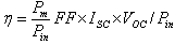 | (2) |
Where Pm is the maximum power of the device and Pin is the incident power[9].
4. Results and Discussion
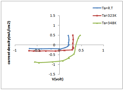
Typical current-voltage (I–V) characteristics of the forward and reverse bias of a SeTe/n-Si heterojunction are shown in Figure 2. In the forward bias, the current increased exponentially along with voltage. However, in the reverse bias, the current increased slowly with voltage (soft breakdown) and did not exhibit any trend of saturation or sharp breakdown[10, 11]. This phenomenon can be attributed to the domination of the edge leakage current caused by the sharp edge at the periphery of the contact as well as the generation of excessive carriers in the depleted region at higher fields.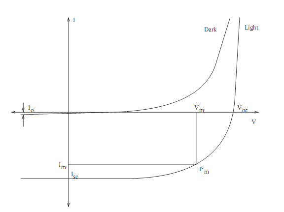 | Figure (1). I–V curve of solar cells in the dark and under illumination |
 | Figure (2). I–V characteristics of a SeTe/c-Si heterojunction solar cell (SeTe thickness = 300 nm) |
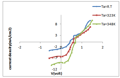 | Figure (3). I–V characteristics of a SeTe/c-Si heterojunction solar cell (SeTe thickness = 600 nm) |
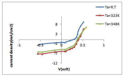
 | Figure (4). I–V characteristics of a SeTe/c-Si heterojunction solar cell (SeTe thickness = 750 nm) |
Figures (2) to (5) show that the Voc and Isc of the SeTe/Si films increase with increasing annealing temperature. This phenomenon can be attributed to the presence of defects that act as capture centers and generate carriers, leading to increases in recombination processes and the current value. The efficiency of the heterojunction produced from the SeTe films also increased with increasing annealing temperature, as shown in Tables (1) to (3). The efficiency of this device further increased with increasing SeTe film thickness up to 600 nm. At 750 nm, however, the efficiency of the heterojunction was less than that at 600 nm.| Table (1). Efficiency values of a SeTe/c-Si heterojunction solar cell (SeTe thickness = 300 nm) |
| | Ta K | η % | | R.T | 0.8 | | 323 | 1.5974 | | 348 | 2 |
|
|
| Table (2). Efficiency values of a SeTe/c-Si heterojunction solar cell (SeTe thickness = 750 nm) |
| |
|
| Table (3). Efficiency values of a SeTe/c-Si heterojunction solar cell (SeTe thickness = 600 nm) |
| |
|
5. Conclusions
A SeTe/n-Si heterojunction was prepared by thermal evaporation to obtain photovoltaic characteristics with efficiencies ranging from 0.8 to 4.1. The efficiency of the resulting heterojunction increased as the annealing temperature and thickness of the SeTe film used increased.
ACKNOWLEDGMENTS
This study was supported by the Renewable Energy Research Center of the University of Anbar-Iraq under Grant No. RERC-TP7.
References
| [1] | Rogacheva, E. I., Nashchekina, O. N., Tavrina, T. V., Us, M., Dresselhaus, M. S., Cronin, S. B., Rabin, O., "Quantum size effects in IV-VI quantum wells", Physica E – Low - Dimensional Systems & Nanostructures,17, (1-4), 313-315, (2003). |
| [2] | Chaya H. Ben-Porat, Oksana Cherniavskaya, Louis Brus, Kyung-Sang Cho, and Christopher B. Murray ''Electric Fields on Oxidized Silicon Polarization of PbSe Nanocrystals'', Journal of Physical Chemistry A. 108, 7814-7819, (2004). |
| [3] | A. Hallbauer, T. Schwarzl, R. T. Lechner and G. Springholz ''Molecular Beam Epitaxy of PbSe1-xTex for Strain Engineering in IV-VI Semiconductor Heterostructures'', Proceedings GMeForu (2003).http://gme.tuwien.ac.at/forum2003/Hallbauer.pdf |
| [4] | P. and Siffert, P. ''Role of oxygen in the mechanism of formatting of Schottky diodes'', Journal of Applied Physics, Vol. 49, Issue 12 6004 (1978);http://dx.doi.org/10.1063/1.324569 |
| [5] | Zogg H. "Epitaxial Narrow gap Lead Chalcogenide Layers on Si-substrates for Infrared Sensor Arrays", Thin Film Physics Group (GruppeDünnschichtphysik) Annual Report, p. 4, (2006). http://gme.tuwien.ac.at/forum2003/Hallbauer.pdf |
| [6] | D.K. Ivanoua, E.A. Streltsova, A.K. Fedotova, A.V. Mazanika, D. Finkb, A. Petrov, "Electrochemical deposition of PbSe and CdTe nanoparticles onto p-Si(100) wafers and into nanopores in SiO2/Si(100) structure" Elsevier, Thin Solid Films 490, pp. 154 –160 (2005). |
| [7] | Sang Yeol Lee, Eun Sub Shim, Hong Seong Kang, Seong Sik Pang, Jeong Seok Kang, "Fabrication of ZnO thin film diode using laser annealing", Elsevier Science Direct, Thin Solid Films 473, pp. 31– 34, (2005) |
| [8] | C. Vijayan, M. Pandiaraman, N. Soundararajan, R. Chandramohan, V. Dhanasekaran, K. Sundaram, T. Mahalingam, and A. John Peter, " Structural and optical properties of Ag2SeTe nano thin films prepared by thermal evaporation " Springer Science, Journal of Material Science: Mater Electron, vol. 22, pp. 545–550, (2011). |
| [9] | V. Viswanathan, "Study Of Cu Free Back Contacts To Thin Film CdTe Solar Cells" Doctoral Thesis, University of South Florida, College of Engineering, (2004).http://scholarcommons.usf.edu/cgi/viewcontent.cgi?article=2284&context=etd |
| [10] | I. M. Ibrahim, "Electrical and Optical Properties of Se-Te-Sb and Se-Te-Ge Thin Films Systems", Ph. D Thesis, University of Baghdad, College of Science, (2009). |
| [11] | Simon M. Sze, Kwok K. Ng, "Physics of Semiconductors Devices, 3 Edition", John wiley and Sons, Newyork, (2006). |
 Abstract
 Reference
 Full-Text PDF
 Full-text HTML