Pankaj R. Patel 1, H. S. Patel 2, J. R. Rathod 3, K. D. Patel 4, V. M. Pathak 4
1Smt S. M. Panchal Science College, Talod, 383 215, Gujarat, India
2Arts, Commerce and Science college, Borsad, 388 540, Gujarat, India
3Dr. JivrajMehta Institute of Technology, Mogar, 388 340, Gujarat, India
4Department of Physics, Sardar Patel university, VallabhVidyanagar, 388 120, Gujarat, India
Correspondence to: Pankaj R. Patel , Smt S. M. Panchal Science College, Talod, 383 215, Gujarat, India.
| Email: |  |
Copyright © 2012 Scientific & Academic Publishing. All Rights Reserved.
Abstract
WSe2 is known to have layered structure with various polytypes having different stacking structures developing on conditions prevailing during the synthesis of crystals. Looking to its potential for application in electronic devices, it will be important to investigate growth conditions vis a vis electrical properties which depends on structure. Crystals of Tungsten Diselenide (WSe2) have been grown by direct vapor transport (DVT) technique using micro processor controlled dual zone horizontal furnace. The chemical composition and structure of grown crystals were confirmed using energy dispersive analysis of X-ray (EDAX) and X-ray diffraction (XRD). In the present investigation thermoelectric power measurements (TEP) have been carried out on the grown crystals. Different electrical transport parameters of semiconductors have been determined and discussed in the paper. The Ohmic nature of contacts prepared for van der Pauw geometry in case of various pairs of contacts at 300 K The ohmic contacts were developed using Ag-paste and the Hall effect measurements have been carried out in the temperature range 50 - 300 K to determine some essential parameters such as the hole mobility (µ), carrier concentration (n), Hall coefficient (RH).Transition metal dichalcogenides materials (TMDCs) use in photovoltaic and photo electrochemical (PEC) solar cells is because of their inherent resistive nature to photo corrosion.
Keywords:
WSe2, Structural, Electrical, EDAX, XRD, TEP, Hall Effect
Cite this paper: Pankaj R. Patel , H. S. Patel , J. R. Rathod , K. D. Patel , V. M. Pathak , Growth, Structural and Electrical Characterization of Tungsten Diselenide Crystals Grown by Dvt Technique, American Journal of Condensed Matter Physics, Vol. 3 No. 1, 2013, pp. 13-20. doi: 10.5923/j.ajcmp.20130301.03.
1. Introduction
In recent years, group- VI semiconductors have attracted much interest in their applications particularly in the area of solar cells. WSe2 is a member of the compounds of VI-A and VI-B group. It has stacked layer structure of M-X-M type which is an extra incentive for device research. Here M is transition metal e.g. tungsten and X is chalcogen e.g. Selenium. The crystal structures of the layered TMDC are usually described as belonging to 1T, 2H, 3R, 4H2, 4Hb, 6R phases[1, 2]. TMDCs have been used for many years as solid state lubricants[3], photovoltaic/photo catalytic solar energy converters[4-7]. Transition metal dichalcogenides materials use in photovoltaic and photo electrochemical (PEC) solar cells is because of their inherent resistive nature to photo corrosion.Looking to potential for such diverse applications of TMDCs, we have chosen to study WSe2 semi-conducting materials of group VI. Successful growth of single crystals of WSe2 has been reported earlier[8] for the measurements of photoelectric and electrical properties. Here we report electrical transport parameters of the well characterized grown crystals of WSe2 have been done. Thermoelectric properties like carrier concentration, Fermi energy, density of states and effective mass of carriers have also been determined and discussed in the paper. Here we report Hall Effect measurements. These investigations can yield valuable information about their electronic properties.
2. Experimental
Crystals of Tungsten dieseline (WSe2) have been grown by direct vapour transport (DVT) technique using dual zone horizontal furnace. The temperature profile used for the growth of WSe2 crystal is shown in fig. 1. The crystals grown were found to be in the form of thin platelets having opaque appearance with silver shining surface. The chemical composition was identified using energy dispersive analysis of X-ray (EDAX) (XL–30 ESEM, Netharland) XRD analysis was carried out by X-ray Diffractometer (Philips, X-pert MPD, Netharland) for the determination of structure. The thermoelectric power measurements (TEP) have been carried out on the grown crystals with the help of totally computer controlled TEP measurement setup developed in our laboratory. 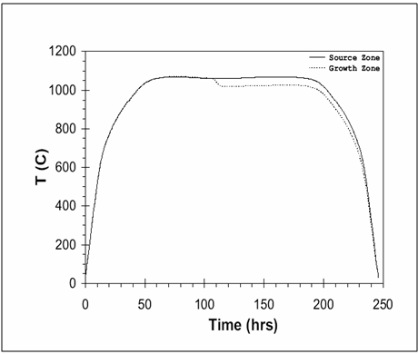 | Figure 1. The temperature profile used for the growth of WSe2 |
The sample with area 3x3 mm2 was used. The measurements were taken in the temperature range of 333K to 473K and the temperature difference (∆T) between the ends of the sample was kept to be 10K. These crystals were also characterized using Hall effect measurement setup (Lakeshore-7504) in temperature range 10 - 300K to estimate the carrier concentration, hole mobility, Hall coefficient and resistivity.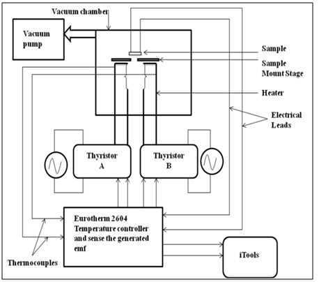 | Figure 2. Block diagram of the equipment setup of thermo electric power measurement |
3. Results and Discussion
3.1. EDAX Analysis
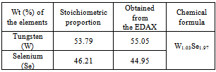
The stoichiometry of the grown crystals was analyzed by EDAX and it is found that thegrown crystals possess nearly perfect stoichiometry with chemical formula W1.03Se1.97. There are no any impurities were presented in the limit of sensitivity.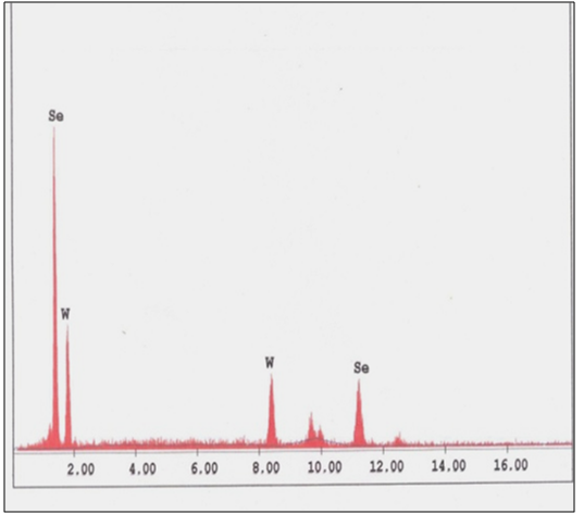 | Figure 3. EDAX Scan of WSe2 crystal |
Table 1. Chemical composition (wt. %) of as grown WSe2 crystals obtained by EDAX analysis with chemical formula
 |
| |
|
3.2. XRD Study
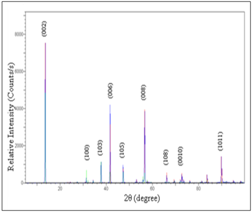 | Figure 4. X-ray diffractogram of WSe2 crystal |
The typical X-ray diffractogram of the grown WSe2 crystal is shown in figure 3.5was obtain with the help of Phillips X’pert MPD X-ray diffractometeremploying Cu, Kα radiation. All the peaks were indexed with the help of "powder X" programme, as depicted in fig.4. The highest intensity peak indicates the most preferred orientation of the crystal grains. The analytical indexing of the pattern thus obtained was done to calculate the lattice parameters for the hexagonal layered structures. The results obtained for as grown crystals of WSe2 are given in table 2. In order to affirm that these lines belong to tungsten diselenide, the d spacing and relative intensities of these lines were compared with JCPDS data 2H-WSe2polytypes[6]. The lattice parameters, a and c, were determined for hexagonal structure using the following equation[4, 5]. | (1) |
where h, k and l represent the Miller indicesand d is the inter planer spacing. Theobserved ‘d’ values and calculated ‘d’values are shown in table 2.The particle size (D) of the WSe2Crystals was determined by using the Debye-Scherrer’s formula, | (2) |
where λ is the wave length of X –rays used, β is the FWHM, k is a constant (taken as 1) and θ is the angle between the incident and scattered X-rays.[10].The micro strain (ε) and the dislocation density (ρ) of the deposited films were evaluated using the equations[11] | (3) |
and | (4) |
The results of these calculations have also been shown in table 2. The data presented in table 2.
3.3. Thermoelectric Power Study
The results of TEP measurements as shown by variation of thermoelectric power (S) with temperature in the range 333K to 750 K have been shown in fig.5. The positive values of ‘S’ shows that the crystals possess p-type conductivity. To analyze the temperature dependence of thermoelectricpower of a p-type semiconductor, the expression given by Mohanchandra and Uchil[12] and H. J. Goldsmid[13] has been used. It is given as | (5) |
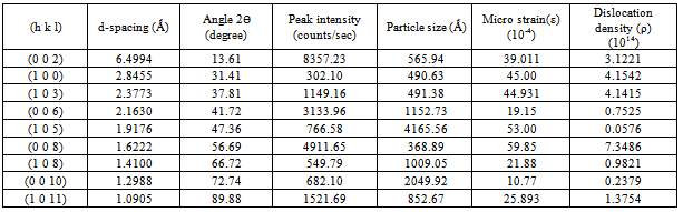
where k is Boltzmann constant, e is electronic charge, A=(5/2 - C) is the scattering coefficient which varies from 0 to 4 depending on the scattering process , C is the scattering parameter and EF is the separation of Fermi level from the top of the valance band.As the carrier concentration depends on EF in the crystal and for a small temperature range, EF can be considered as fairly constant, equation (1) can be expressed as[14 – 17]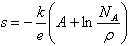 | (6) |
Here NA=[2πmh*kT/h2]3/2is the effective density of states inwhich mh* is the effective mass of holes and h is the Plank’s constant.Considering constant EF, theplot of thermoelectric power (S) against the reciprocal of temperature gives a straight line as shown in fig. 5.
3.4. Low Temperature Hall Effect
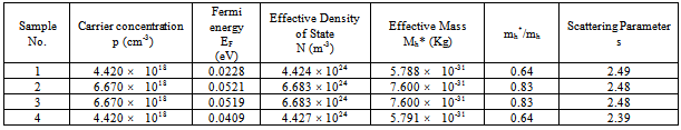
The Ohmic nature of contacts prepared for van der Pauw geometry in case of variouspairs of contacts at 300 K is shown in the Fig. 6. It is seen from here that Ag-pastecontacts exhibit good Ohmic nature for both polarity in a large current range. The average van der Pauw factor for a set of four contacts is found to be 0.7. This deviationfrom ideal requirement of unity probably originates from the anisotropic nature of WSe2 and not from other conditionsrequired for measurements using van der Pauw technique.The resistivity (p), Hallcoefficient (RH), carrier density (n) and mobility (u) of WSe2 single crystals were calculated from the measured I - V values under magnetic field of 3kG using thestandard formula over the temperature rangeof 50K to 300K and the results are tabulated in Table - 4. Figs. 7 and 8 show the variation of Resistivity, Hall Coefficient and Carrier concentration with respect to inverse of temperature. From these figures it is clearly seen that resistivity is decreasing monotonically with increasing temperature above around 90K which confirms the semiconducting nature of WSe2 crystals.The anomalous semiconducting behavior below 90K is reflected in mobility also andseems to be related to changes in scattering mechanism. However carrier concentration is increasing with increasing temperature.Table 2. Structural parameter for WSe2 Crystal
 |
| |
|
Table 3. Carrier Concentration, Fermi Energy, Effective Density of State, Effective Mass, Scattering Parameter of WSe2crystal
 |
| |
|
Table 4. Measured Hall parameters of WSe2 crystal
 |
| |
|
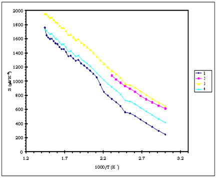 | Figure 5. Variation of thermoelectric power S of WSe2 single crystal as an inverse function of temperature (ΔT = 10 K) |
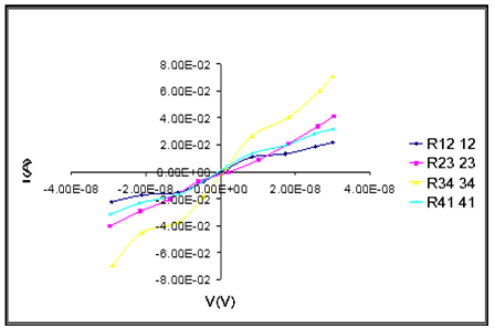 | Figure 6. I-V characteristics between different pair of contacts for p-WSe2 crystal |
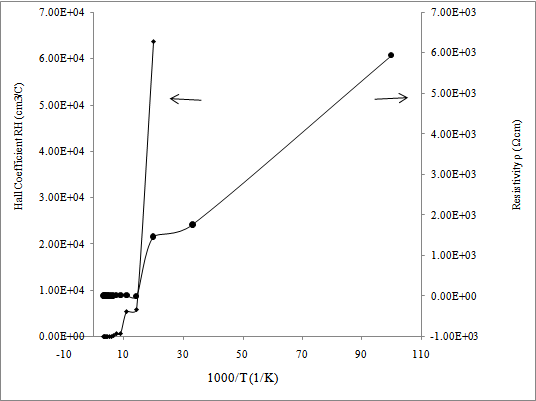 | Figure 7. RH andρ of p-WSe2crystals as a function of 1000/T |
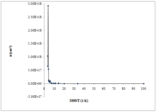 | Figure 8. Carrier concentration vs. 1000/T for p-WSe2crystal |
4. Conclusions
The EDAX analysis shows that the grown crystals are nearly perfect in stoichiometry. The X-ray analysis shows that crystals posses hexagonal structure. The values of the computed lattice parameters for the grown crystals are a = b = 3.28Å and c = 13.00 Å. The single crystals of WSe2 grown by a direct vapour transport technique are found to have a p- type (WSe2) semiconducting nature. The value of scattering parameter is nearly ≈ 2.48 which shows that the defect scattering dominates the charge transport mechanism in the grown crystals. The value of effective density of states is found to be around 6.68x1024 m-3. The effective mass of charge carriers mh* was calculated and is found to be around 7.6x10⁻³¹ Kg. All these estimated parameters are in good agreement with the reported values in the literature[11-13].The sign of Hall coefficient remains positive in the entire range of measurement temperature, indicating the conductivity type of the crystals as p-type and it is in agreement with the TEP measurements. This again shows that the quality of ohmic contacts made for present investigations is good and stable throughout the range of reported measurements. The conductivity of the sample decreases with the temperature and thus again confirms the semiconducting nature of the grown WSe2 crystals. The measured carrier concentration at room temperature is 1.032x1018 cm-3. This is in agreement with the reported value of 3.5x1018 cm-3[14].
References
| [1] | Deshpande M. P., Agarwal M. K., Patel P. D. and Laxminarayana D.,[1999]Depandance of the electrochemical behavior of p-WSe2 single crystals on ohmiccomtactsJournal of materials science letters,18, 233. |
| [2] | Retterberger Armin and Leiderer Paul.[1997] Ultrafast electron transport in layered semiconductors studied with femtosecond-laser photoemission, Phys. Rev. B 56, 12092. |
| [3] | Agarwal M. K. , Patel P.D., and Gupta S. K.[1993]Photovoltaic study of WSe2 Crystals, Journal of Crystal Growth129,559. |
| [4] | Cullity B D, Elements of X-ray diffraction,[1978] 2nd Edition, (Addision-Wesley, USA) 189. |
| [5] | Suryanarayana C, Grant Norton M, X-ray diffraction A practical approach, (Plenum Press, New York) (1998) 125. |
| [6] | JCPDS, International Centre for Diffraction Data,[1997] PDF-2 File No. 38-1388 (WSe2). |
| [7] | Coheroon R, Haas C, Dijkstra J, Flipse C J F, de Groot R A,Wold A.[1987] Synthesis and optical properties of MoS2 and isomorphousnanoclusters in the quantum confinement regime, Phys.Rev. B, 35 6195. |
| [8] | Finteis T, Hengsberger, Straub T, Fauth K, Claesen R, Auer P, Steiner P, Hüfner S, Blaha P, Vögt M, Lux-Steiner M, Bucher E.[1997]Electron spectroscopy applied to low dimemsional material Phys. Rev. B, 55 10400. |
| [9] | Murray R, Evans B L.[1976]Anisotropic mean-square displacements (MSD) in single-crystals of 2H- and 3R-MoS2, J.Appl.Crys., 12312. |
| [10] | Schellenberger A, Schalf R, PettenKofer C, Jaegermann W.[1992] Synchrotron-induced surface-photovoltage saturation at intercalated Na/WSe2 interfaces, Phys. Rev. B, 453538. |
| [11] | Patel H. S. ,Rathod J. R., Patel K. D., PathakV. M. [2012] Structural and Surface Studies of Vacuum Evaporated Cadmium Telluride Thin FilmsAmerican Journal of Materials Science and Technology 111-21. |
| [12] | Goldsmid H. J.[1950]Apllications in Thermoelectricity, Methuen Monograph, London. |
| [13] | Solanki G. K., Gujarathi D., Deshpande M. P., Laxminarayana D. and Agaawal M. K..[2008]Thermo electric properties of WSe2 crystalsCryst.Res. Techol. 43(2), 179. |
| [14] | VoraMihir M, VoraAditya M,[2007] Stacking Faults in Re doped MoSe2 Single Crystals, Chalco. Lett., 4 77. |
| [15] | Lee P A, Said G, Devis R, Lim T,[1969]Structural and electronic properties of ZrX2 and HfX2 (X = S and Se) from first principles calculationsJ. Phys. Chem. Sol., 30 2719. |
| [16] | Lee P A, Said G, Devis R, Lim T.[1969] Negative resistance and switching effect in the single crystal layer compounds SnS2 and ZrS2, Solid SatateCommun., 7 1359. |
| [17] | Patel S G, Agrwal M K, Batra N M, Lakshminarayana D.[1998] Electrical properties of Zirconium Diselenide single crystals Grown by iodine transport method Bull. Mater. Sci., 21, 213. |
| [18] | Solanki G K, Gujarathi D N, Deshpande M P, Laxminarayana D, Agrawal M K.[2008] Transport property measurements in tungsten sulphoselenide single crystals grown by a CVT technique, Cryst. Res. Technology,43(2) 179. |
| [19] | Perluzzo G, Lakhani A A, Jandl S,[1980]Electrical transport measurements in a quasi-one dimensional semiconductor ZrS3, Solid State Communication, 35 301. |
| [20] | Singh J P,[1995] 24 Size Effects in Gas-Phase Photo-oxidation of Trichloroethylene Using Nanometer-Sized TiO2 CatalystsJ. Mater. Sci. Mater. Electron, 2 105. |
 Abstract
 Reference
 Full-Text PDF
 Full-text HTML