-
Paper Information
- Previous Paper
- Paper Submission
-
Journal Information
- About This Journal
- Editorial Board
- Current Issue
- Archive
- Author Guidelines
- Contact Us
American Journal of Condensed Matter Physics
p-ISSN: 2163-1115 e-ISSN: 2163-1123
2012; 2(3): 73-76
doi: 10.5923/j.ajcmp.20120203.04
The Effect of Annealing on the Size and Morphology of Palladium Nanopaticles
 Abstract
 Reference
 Full-Text PDF
 Full-Text HTML
Feridoun Samavat , Parisa Taravati Ahmad , Farzane Mahmoodi , Mohammad Faraz Samavat , Mohammad Hossein Tavakoli
Department of Physics Bu-Ali Sina University, Hamedan, 65174, Iran
Correspondence to: Feridoun Samavat , Department of Physics Bu-Ali Sina University, Hamedan, 65174, Iran.
| Email: |  |
Copyright © 2012 Scientific & Academic Publishing. All Rights Reserved.
Palladium(Pd) nanoparticles are produced by variety of methods. In this research, at first Pd nanoparticles were produced by electron beam coating method and then morphology of Pd nanoparticles were studied. Obtained coating can be used as active layer in hydrogen and hydrogen compounds sensors or in hydrogen storage applications. The characterization of the Pd film has been performed by various techniques such as XRD and SEM. The texture and morphology of the materials has been investigated by Atomic Force Microscopy(AFM). Results of different analyses on the Pd films show that the increasing of annealing temperature could increase the Pd nanoparticles size.
Keywords: Coating Deposition, Metal Nanoparticle, Thin Films, Structure and Morphology, XRD, SEM, AFM
1. Introduction
- In recent years, there has been enormously wide-spread interest in nano-materials and their size-dependent properties. It is well known that metal particles of nanometer size have unique characteristics that differ from those of individual atoms and bulk materials[1]. Thin films of metal nanoparticles have been receiving increasing attention because of the optical, electronic and catalytic properties of such materials[2,3].Thin films of palladium(Pd) and its alloys are used in a variety of technologically important applications including catalysis, gas sensors, and hydrogen permselective membrane[4-7]. In case of nanoporous coating based on palladium nanostructures high efficiency of adsorption /desorption processes and reactivity of Pd toward hydrogen allow for applications of such coatings in hydrogen detectors[8]. It is well known that the optical properties of noble metals are improved by obtaining them in nanosized particulate films with a reference to specific applications[9].Nanostructured palladium particles, because of their high activities toward oxygen reduction reactions, have attracted much attention in recent years as cathode catalysts for fuel cell applications[10]. Moreover, considerable effort has been focused on the synthesis of palladium nanoparrticles[11-13]. Special techniques are needed to synthesize materials with particle size in the nanometer range. Morphology of such materials are studied by SEM and AFM[14]. In thispaper, thin film palladium on glass/silicon substrate is de posited by the electron beam coating method. The films are subsequently reduced to form nanoparticulat palladium film by increasing temperature.
2. Experiments
- Primary material used in this survey, palladium(99/95% pure) was bought from goodfellow Co. The Pd films were prepared by electron beam coating method on glass substrates. These substrates were cleaned with ultrasonic apparatus prior to deposition.Typical coating parameters were cathode voltage 8.5 kV, pressure 3×10⁻⁵ torr, substrate temperature 32℃, coating rate 12A0S-1 and film thickness about 123A0.Then samples were exposed temperature. The temperatures of annealing process were 450℃, 550℃ and 650℃. The structure characterizations of the thin films were obtained by X-ray diffraction. The Pd nanoparticles formed and the fine structure of the Pd was observed by using SEM and AFM.
3. Results and Discussion
- Fig.1 illustrates a typical X-ray diffraction(XRD) pattern of the obtained thin films palladium. These patterns show effect of annealing on layers crystallite properties. The wide peak present in XRD pattern(a) proves that exists amorphous structure in sample in room temperature. These patterns show that with increasing temperature, intensity of obtained peaks increases and its width decreases, indicating formation of crystallite and nanoparticles diameter increase with increasing temperature. In the patterns no impurity phases can be detected. All the diffraction peaks can be assigned to{004}, {111}, {200}, {220} planes respectively for palladium.
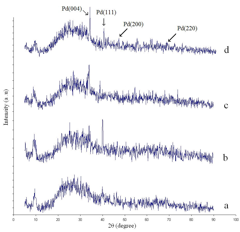 | Figure 1. X-ray diffraction(XRD) pattern for Pd films at a) the sample without annealing and different temperature b) 450℃ , c) 550℃ , d) 650℃ |
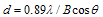 , where λ is the x-ray wavelength(), θ is the Bragg diffraction angle and B is the peak width at half-maximum. Mean crystallite size was obtained by measuring the broadening of the {004} diffraction peak and applying the x-powder software. The average crystallite size were: 3nm, 6nm and 19nm for the sample in 450℃, 550℃ and 650℃ respectively.The obtained structure and topography of coating were studied by SEM and AFM. Fig.2 shows the scanning electron micrographs for thin films palladium in difference annealing temperature. Present SEM images show a grain structure for Pd films, and the size of grains were higher with increasing of annealing temperature. The particles formed showed sizes of 44nm, 53nm and 286nm for 450℃, 550℃ and 650℃ respectively. These results are in agreement with XRD results.Fig. 3 shows topography of two dimansions and three dimansions annealed films in temperatures 450℃, 550℃ and 650℃. The Atomic Force Microscopy(AFM) images confirmed results previous experimental that with temperature increasing increases crystal structure.
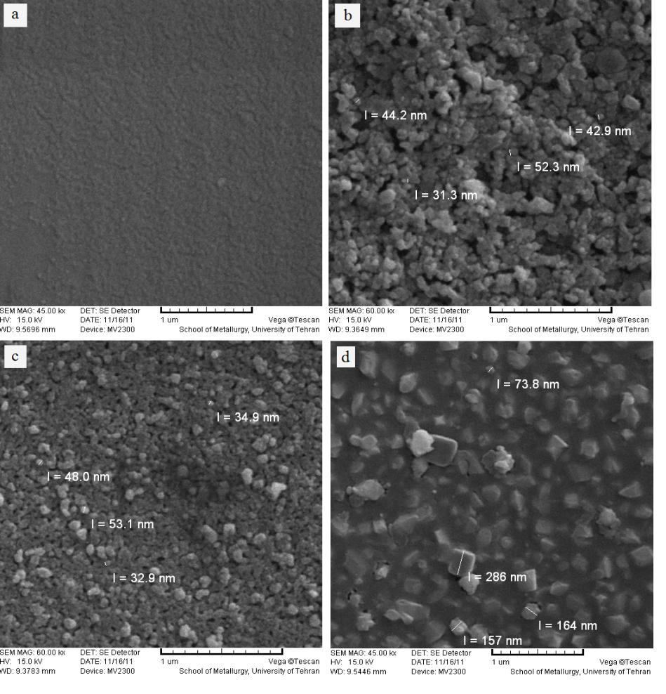 | Figure 2. SEM images of Pd films from a) sample without annealing and different temperatures b) 450℃, c) 550℃, d) 650℃ |
 | Figure 3. AFM images of Pd films from a) the sample without annealing and different temperatures b) 450℃, c) 550℃, d) 650℃ |
4. Conclusions
- In summary, Pd coating was obtained by electron beam on glass substrates. XRD results show that this film has amorphous structure at room temperature. Also, XRD patterns show that crystal grains are forming with the annealing and with increasing temperature, increase grains size. AFM and SEM results confirm it.