-
Paper Information
- Next Paper
- Paper Submission
-
Journal Information
- About This Journal
- Editorial Board
- Current Issue
- Archive
- Author Guidelines
- Contact Us
American Journal of Condensed Matter Physics
p-ISSN: 2163-1115 e-ISSN: 2163-1123
2012; 2(1): 1-10
doi:10.5923/j.ajcmp.20120201.01
Computational Investigation of Electronic and Optical Properties of Si, Ge and Si1-xGex Alloys Using the FP-LMTO Method Augmented by a Plane-Wave Basis
 Abstract
 Reference
 Full-Text PDF
 Full-text HTML
K. Zellat1, B. Soudini1, N. Sekkal2, S. M. Ait Cheikh3
1Applied Materials Laboratory (AML), University of Sidi Bel Abbès, Sidi Bel Abbès, 22000, Algeria
2Département de Physique-Chimie, Ecole Normale Supérieure de l’Enseignement Technique, Oran, 31000, Algeria
3Lab. de Dispositifs de Communication Conversion Photovoltaique , Ecole Nationale Polytechnique, Alger, Algeria
Correspondence to: B. Soudini, Applied Materials Laboratory (AML), University of Sidi Bel Abbès, Sidi Bel Abbès, 22000, Algeria.
| Email: |  |
Copyright © 2012 Scientific & Academic Publishing. All Rights Reserved.
An investigation into the structural, electronic and optical properties of Si, Ge, and Si1-xGex for different compositions was conducted using first-principles calculations based on density functional theory (DFT). The total energies were calculated within the full -potential linear muffin-tin orbital (FP-LMTO) method augmented by a plane-wave basis (PLW), implemented in Lmtar code. The effects of the approximations to the exchange-correlation energy were treated by the local density approximation (LDA). From our simulation results, it is found that the theoretical ground-state parameters, the band structure, the density of states (DOS), the chemical bonding and the optical properties agree well with the experiment and other theoretical calculations. The accuracies found from the present calculations allow us to describe the properties of the electronic as well as the optoelectronic devices based on the Si1-xGex alloy.
Keywords: FP-LMTO Calculation, Electronic Properties, Optical Properties, Si1-Xgex Alloy
Cite this paper: K. Zellat, B. Soudini, N. Sekkal, S. M. Ait Cheikh, Computational Investigation of Electronic and Optical Properties of Si, Ge and Si1-xGex Alloys Using the FP-LMTO Method Augmented by a Plane-Wave Basis, American Journal of Condensed Matter Physics, Vol. 2 No. 1, 2012, pp. 1-10. doi: 10.5923/j.ajcmp.20120201.01.
Article Outline
1. Introduction
- Semiconductors have played a major role in the current technological revolution. For the past years, a major aspiration of condensed matter physics has been to explain and predict the properties of solids knowing only the identities of the constituent atoms. Recently, this goal has been realized for many semiconductors properties. The successes are best illustrated by the progress made in understanding the structural, electronic and optical properties of semiconductors.Among semiconductors, the covalent semiconductors Si and Ge have been studied extensively both theoretically and experimentally[1,2] Group IV semiconductor alloy like Si-Ge, have the immense potential for technological applications[3-5].Silicon Germanium (Si1-xGex) alloy is good candidate as a substitute material for Si in low-power and high-speed semiconductor device technologies[6]. Optoelectronic devices, such as heterojunction bipolar transistors, are already in industrial production. Si1-xGex is also promising as alloying material for quantum well devices, for the 1.3-1.55 μm optical communication detectors[7,8] for the 2 μm to 12 μm infrared detectors[9,10], and modulation-doped field-effect transistors[11]. The main reason for this is the requirement of the direct gap materials for fabrication of optoelectronic devices. The system, for example, Si-Ge improves the transport and optical properties as compared to silicon. Due to such applications of the system in optoelectronics devices, the theoretical and experimental studies of Si-Ge system is an important task. The number of bonding electrons does not change when the solid solution of Si1–xGex is formed and, hence, the theoretical study of the system of Si-Ge solid solutions is also interesting.Although much efforts have been paid on the growth of Si1-xGex and Si1-xGex /Si as well on electrical characterization, there is still a lack of information about the optical properties of Si1-xGex . This prompts us to study these proprieties in the present work.The main goal of this paper is to provide a consistent and complete set of electronic and optical parameters that are need for our next quantitative calculations of the quantum cascade laser (QCL) properties based on these materials.This paper is organized as follows. In Section 2 we describe the theoretical methodology of the first principles calculations and discuss the details of the calculations. The results of the band structure, the density of states (DOS), the chemical bonding and the optical properties are presented and discussed in Sec. 3. Finally, Section 4 summarizes the paper.
2. Method of Calculations
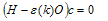
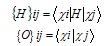
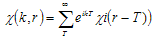
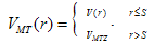
- In this work, full potential linear muffin -tin orbital (FP-LMTO) method, as employed in the lmtart code[12-14], has been applied to perform first -principles total energy calculations. It’s a specific implementation of density functional theory within the local density approximation (LDA). In this method, there is no shape approximation to the crystal potential, unlike methods based on the atomic-spheres approximation (ASA) where the potential is assumed to be spherically symmetric around each atom. For mathematical convenience the crystal is divided up into regions inside muffin-tin spheres, where Schrödinger's equation is solved numerically, and an interstitial region.In all LMTO methods the wave functions in the interstitial region are Hankel functions. Each basis function consists of a numerical solution inside a muffin-tin sphere matched with value and slope to a Hankel function tail at the sphere boundary. The so-called multiple-kappa basis is composed of two or three sets of s, p, d, etc. LMTOs per atom. The extra variational degrees of freedom provided by this larger basis allow for an accurate treatment of the potential in the interstitial region. One advantage of this method over, pseudopotential-based methods, in the context of high-pressure physics and elsewhere, is that the core and semi-core electrons are explicitly included in the calculations. In addition, to first order all materials require equal computational effort, with no dependence on a deep versus shallow pseudopotential. However, pseudopotential based methods are generally much more computationally efficient for large numbers of atoms, due in part to a simpler mathematical foundation that is more amenable to clever algorithmic shortcuts. In order to solve the Kohn-Sham (KS) equation, the wave function needs to be expanded in a known basis set {χ} in the following form:
 | (1) |
 | (2) |
 | (3) |
 | (4) |
 | (5) |
 | (6) |
 | (7) |
3. Results and Discussions
3.1. Electronic Band Structure of Si and Ge
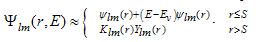
- Energy bands consisting of a large number of closely spaced energy levels exist in crystalline materials. The bands can be thought of as the collection of the individual energy levels of electrons surrounding each atom. The wavefunctions of the individual electrons, however, overlap with those of electrons confined to neighbouring atoms. The Pauli Exclusion Principle does not allow the electron energy levels to be the same so that one obtains a set of closely spaced energy levels, forming an energy band. The energy band model is crucial to any detailed treatment of semiconductor devices. It provides the framework needed to understand the concept of an energy band gap and that of conduction in an almost filled band as described by the empty states. The energy band diagrams of semiconductors are rather complex[21].The detailed energy band diagrams of silicon and germanium are shown in Figure 1.The energy is plotted as a function of the wavenumber, k, along the main crystallographic directions in the crystal, since the band diagram depends on the direction in the crystal. The energy band diagrams contain multiple completely-filled and completely-empty bands. In addition, there are multiple partially-filled band.One can notice from the figure 1 that the smallest band gap of germanium and silicon are indirect, The values of these gaps turns out to be at 300K, 1.2eV and 0.661eV, respectively. At the same temperature, the energies corresponding to critical points for silicon are EL=2.0eV, EX= 1.2eV, EГ1= 3.4eV. We have found an energy separation (EГL or EГ2) equal to 4.2eV, and an energy spin-orbital splitting Eso equal to 0.044eV. For the germanium at the same temperature, we have EX =1.2eV, EГ2=, 3.22eV, an energy separation (EГ1, ∆E>) = (0.8eV, 0.85eV) and an energy spin-orbital splitting Eso = 0.29eV.With the LMTO (LPW) method, we found for Si, the values of muffin -tin spheres (MTS) , Spheres asa, Nrad= 2.221, 3.1823, 276 respectively . For Ge : MTS, Spheres asa, Nrad = 2.31, 3.3126, 3.32, respectively.
 | Figure 1. The calculated electronic energy-band structure of Si (a) and of Ge (b) |
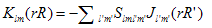
 | Figure 2. Contribution from the different atomics orbital to the electronic energy-band structure for Si (c) and for Ge (d) |
3.2. Electronic Band Structure of the Si1-xGex Alloy
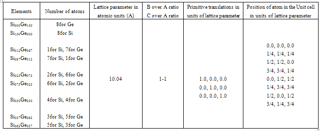
- The next step of our calculations is to show how the stochiometries could affect the band structure of the alloy based on the studied elemental semiconductors. The atom specific data of Si1-xGex alloy are given in Table 1.
|
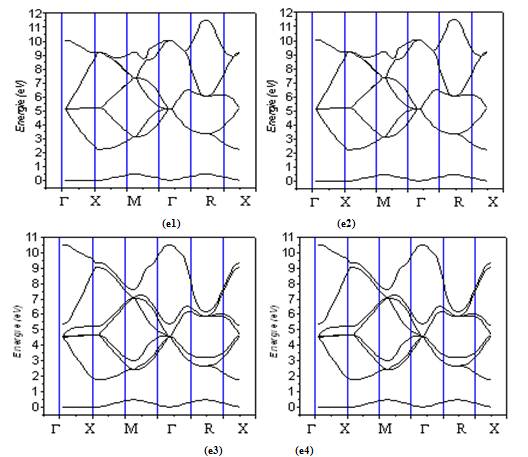 | Figure 3. The calculated electronic energy-band structure of Si1-xGex alloy for Si000Ge100 (e1) , Si100Ge000 (e2),, Si013Ge087 (e3), and Si088Ge012 (e4) |
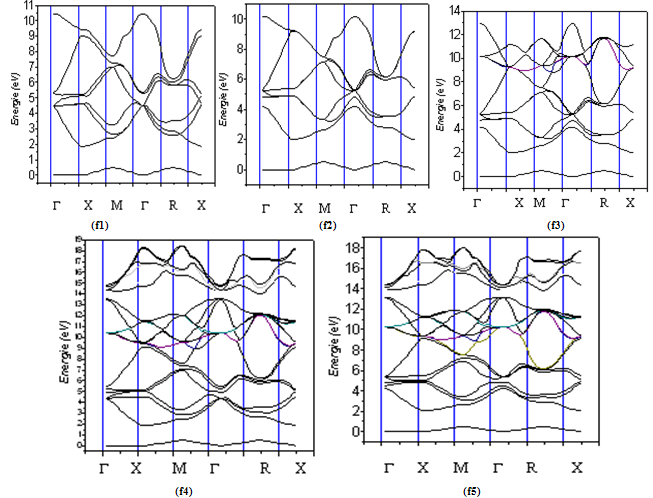 | Figure 4. The calculated electronic energy-band structure of Si1-xGex alloy for Si025Ge075 (f1) , Si075Ge025 (f2),, Si050Ge050 (f3), Si038Ge062 (f4) , and Si063Ge037 (f5). |
3.3. Electronic Charge Density of the Si1-xGex
- To analyze the bonding properties, we have shown in Figure 5 ((1) and (2)) the electronic charge densities of Si and Ge, respectively.It is well known that all properties of a microscopic system of N particles, e.g. charge densities can be obtained from the solution of Schrödinger's equation, but assuming a macroscopic crystal (N approx. 1024) the equation can not be solved. Using the density functional theory of Kohn, and Sham[26,27], Schrödinger's equation can be transformed into a system of 1024 one-particle-equations, and each particle suffers from an effective potential Veff(r). Our calculation method LMTO is based on the Kohn-Sham theorem .In figures 6 ((1) to (4)), we have illustrated the electronic charge densities of Si000Ge100, Si100Ge000, Si050Ge050, Si037Ge062 respectively. Using the other concentration (75%, 87%), we found the same graphs as for the Si050Ge050 alloy.
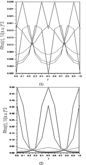 | Figure 5. The calculated electronic charge densities of Si (1) and Ge (2) |
3.4. Density of State of the Si1-xGex Alloy
- In and , the density of states (DOS) of a system describes the number of states at each energy level that are available to be occupied. A high DOS at a specific energy level means that there are many states available for occupation. A DOS of zero means that no states can be occupied at that energy level.As was illustrated in Figure 7, the Fermi level is shifted to 0 eV. We show here the total DOS (sum of all basis which is considered in both atoms) that has considerable contribution towards total density of states. Our calculations for the total DOS of Si000Ge100 yield main structure at 17eV and 26eV above the Fermi level and for Si050Ge050 at11eVand 17eV, for Si075Ge025 at 12.5eV and 17 eV, Si037Ge062 at 11eV and 15.5eV, Si087Ge012 at 11eV and 15.5eV and 23eV above the Fermi level (See figures 5,6,7,8,9), respectively).
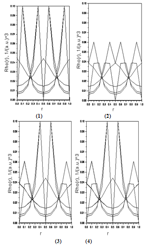 | Figure 6. The calculated electronic charge densities of Si000Ge100 (1) , Si100Ge000 (2), Si050Ge050 (3), and Si037Ge062 (4) |
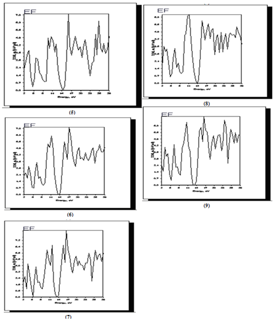 | Figure 7. The calculated total DOS for Si000Ge100 (5), Si050Ge050 (6), Si075Ge025 (7), Si037Ge062 (8) and Si087Ge012 (9) |
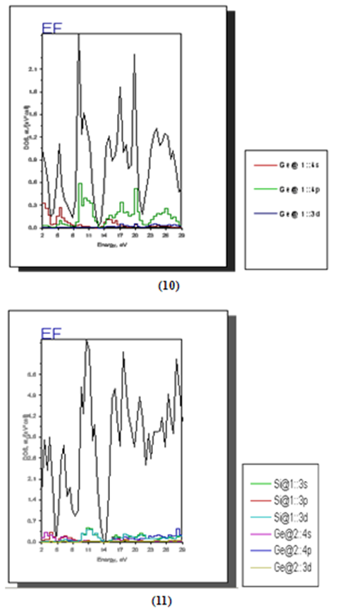 | Figure 8. Contribution of different atomic orbital to the DOS for Ge (10) and for Si025Ge075 (11) |
3.5. Optical Properties of the Si1-xGex Alloy
- It is well known that the basic optical properties of semiconductors result from the electronic excitation in crystals when an electromagnetic wave is incident on them. The calculation of the optical properties of the solids is beset with numerous problems. The knowledge of the dielectric functions ε(E)= εr(E)-iεi(E) allows to describe the optical properties of the medium at all phonon energies E.Calculations of the dielectric function involve the energy eigenvalues and the electron wave functions. These are the natural output of the ab initio band structure calculation which is usually performed under local density approximation (LDA)[29,30] In the LMTO–LPW, we have calculated the frequency dependent imaginary dielectric function, real dielectric function, and electron energy loss spectrum. The effects of using K points in the BZ have already been discussed in the earlier work by Khan et al (1993) [31].Before presenting the results for Si1-xGex alloy with different concentration, we will establish the reference of the optical results for Si and Ge. as depicted in Figure 9(12) and Figure 9(13), respectively.
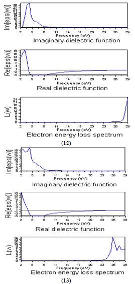 | Figure 9. The calculated frequency dependent dielectric function and electron energy loss spectrum for Si(12) and Ge (13) |
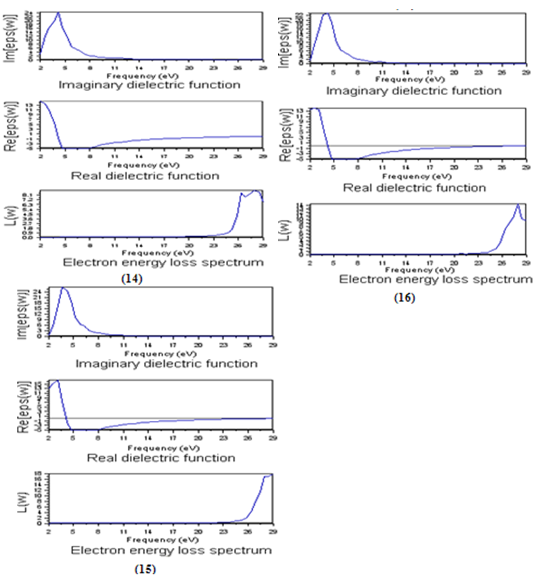 | Figure 10. The calculated frequency dependent dielectric function and electron energy loss spectrum for Si025Ge075 (14), Si075Ge025 (15) and Si050Ge050 |
4. Conclusions
- We have made a detailed investigation of the electronic structure and optical properties of Si, Ge and Si1-xGex alloy using the full-potential linear muffin-tin orbital (FP- LMTO) augmented with the plane wave approximation (PLW). The effect of the approximation to the exchange-correlation energy were treated by the local density approximation (LDA). From the simulation results, it is found that the theoretical ground-state parameters, the band structure, the density of states (DOS), the chemical bonding and the optical properties agree quite well with experimental information as well other theoretical works. In the present work, we have also checked the transferability of the considered calculation method to predict the structural, electronic and optical properties for Si1-xGex alloy from those of their parent semiconductors. Finally, one can deduced from these results that the weakly straind G-rich SiGe layers possess very promising properties for both electronic and optical applications. Further work is in progress.