Srilatha C 1, Guru Rao C V 2, Prabhu G Benakop 3
1Department of ECE, ASTRA, Hyderabad, 500008, India
2Department of CSE, SR Engineering College, Warangal, 506015, India
3Department of ECE & Principal, ATRI, Hyderabad, 500039, India
Correspondence to: Srilatha C , Department of ECE, ASTRA, Hyderabad, 500008, India.
| Email: |  |
Copyright © 2012 Scientific & Academic Publishing. All Rights Reserved.
Abstract
Any embedded system contains both on-chip and off-chip memory modules with different access times. During system integration, the decision to map critical data on to faster memories is crucial. In order to obtain good performance targeting less amounts of memory, the data buffers of the application need to be placed carefully in different types of memory. There have been huge research efforts intending to improve the performance of the memory hierarchy. Recent advancements in semiconductor technology have made power consumption also a limiting factor for embedded system design. SRAM being faster than the DRAM, cache memory comprising of SRAM is configured between the CPU and the main memory. The CPU can access the main memory (DRAM) only via the cache memory. Cache memories are employed in all the computing applications along with the processors. The size of cache allowed for inclusion on a chip is limited by the large physical size and large power consumption of the SRAM cells used in cache memory. Hence, its effective configuration for small size and low power consumption is very crucial in embedded system design. We present an optimal cache configuration technique for the effective reduction of size and high performance. The proposed methodology was tested in real time hardware using FPGA. Matrix multiplication algorithm with various sizes of workloads is hence validated. For the validation of the proposed approach we have used Xilinx ISE 9.2i for simulation and synthesis purposes. The prescribed design was implemented in VHDL.
Keywords:
Cache, Access Time, Miss Rate, Performance
1. Introduction
In today's embedded systems, memory represents a major bottleneck in terms of cost, performance, and power. To overcome this, effective customization of memory is mandatory. Memory estimation and optimization are crucial in identifying the effect of optimization methodology on the performance and energy requirements of the system, in turn obtaining a cost effective embedded system[1]. Figure 1 shows the basic processor architecture. It consists of a main memory module (DRAM), whose performance is far behind that of the connected processor.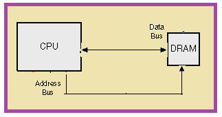 | Figure 1. Basic processor architecture |
One of the solutions to reduce this bottleneck is to employ a cache memory (SRAM) in between the main memory and the processor as shown in figure 2, as SRAM cells have faster access time than DRAM. Also, it helps in improving the overall system performance. 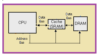 | Figure 2. Basic processor architecture with SRAM |
The SRAM cache memory allows faster memory access time compared to DRAM memory access time, but comes at the expense of larger energy consumption per access. The CPU can access the main memory (DRAM) only via the cache memory (SRAM). The cache memory is transparent to the application being executed in the CPU. Cache memories are used in almost every processor which exists today. Cache memory is included in a system with the purpose of exploiting spatial and temporal locality exhibited by the application’s memory access behavior. The size of cache allowed for inclusion on a chip is limited by the large physical size and large power consumption of the SRAM cells used in cache memory. Figure 2 shows architecture with one level of cache memory. To facilitate the design space exploration steps, a crude performance and energy model for the system was created. The model of the embedded system architecture consisted of a processor with an instruction cache, a data cache, and embedded DRAM as main memory. The data cache uses a write-through strategy. The system architecture is illustrated in Figure 3. As the instruction cache is accessed on every clock cycle, it consumes more energy than the data cache.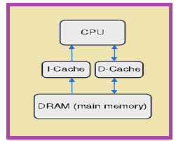 | Figure 3. System architecture |
Thus the addition of high speed SRAM modules as cache memory improves the processor performance. But this also causes the system’s nature to become unpredictable as it cannot be guaranteed whether a memory request will result in a cache hit or a miss. Also, several studies have shown that cache memories account for about 50% of the total energy consumed in embedded systems[2]. Hence, customization of cache memory is very important in meeting tough design metrics like cost, performance and energy consumption. Basically the performance strategy of any program on today’s processors mainly rely on the caches. Hardware improvements especially the cache associativity is the main source of greater efficiency. Program performance is strongly dependent on instruction cache behavior[3], suggesting an opportunity for general improvement. Thus the memory performance can be only measured in terms of time to service the request generated by the processor.
2. Previous Work
Various methodologies have been evolved for the cache analysis for reducing energy by modifying the lookup procedure. Way predictive set-associative caches[4,5] access one tag and one data array initially and only access the other arrays if that initial array does not result in a match, again resulting in less energy at the expense of longer average access time. Existing methodologies for cache miss rate estimation use heuristics to search through the cache parameter design space[6-8]. Speculative way selection can be done either using locality information[9,10] or partial tag comparison[11]. But when the way prediction is wrong, it can result in performance penalty. But our proposed methodology employs the utilization of the XOR functionality implementation for prediction.
3. Cache Organization
The contents of a cache memory is stored as set of cache lines. In other words, cache line size can be defined as the cache location having fixed data width. The cache line size specifies the minimum number of bits that is to be written into the cache for each write request. These cache lines store data of the lower memory level. An instruction cache having a line size (l) of four, stores instructions in each of this line. This four lines constitute a program line when they are in main memory as they form a part and portion of some other large program. In case of a direct mapping, each of the program line is mapped into cache line. The following figure 4 shows the direct mapped cache: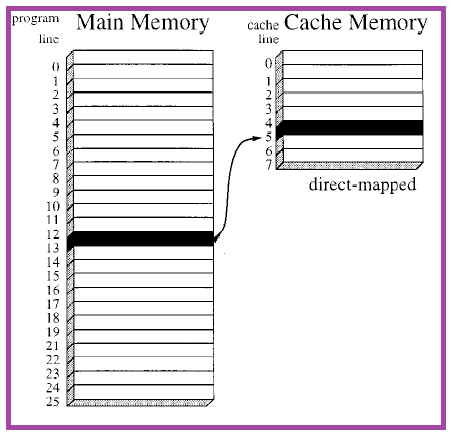 | Figure 4. Direct Mapped Cache |
Assuming L to be the number of lines in the cache and A to be the starting address of the program line, the cache line size l is given by:l=A mod LIn the above direct mapping cache, cache line size can be calculated as 13 mod 8 which equals to five.In case of a fully associative cache, the program line can be mapped to any of the cache line as shown in figure 5.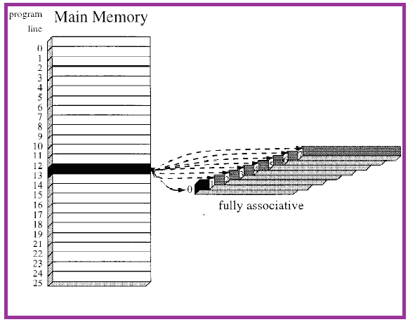 | Figure 5. Fully associative cache |
Mapping the program line into set of n different cache lines is known as set-associative mapping. The following figure 6 shows the mapping technique. Assume S to be the number of cache sets. Let a program line is placed be placed at s set being determined as:s = A Mod SFrom fig. 3, s value can be calculated as s = 13 mod 4 = 1, in other words it is cache line 2 or 3.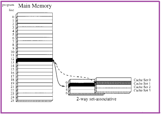 | Figure 6. Set-associative mapping |
With n way set associative cache memory, the cache replacement policy determines which cache location is to be replaced each time a new data is to be written into the cache memory. Typical cache replacement algorithms are round- robin and Least Recently Used algorithms.
4. Performance Analysis
High performance being the key focus entity in designing the memory hierarchy, vast study and research work is carried out to explore the memory subsystem configuration. As a part of this, we have performed cache studies targeting low access time and high performance. The cache access time can be mathematically depicted as:Taccess = [Thit]+ [Tpenalty * M]Where, Taccess = cache access timeThit = cache hit timeTpenalty = miss penaltyM = miss rateAccess TimeThe access tome in a cache memory can be lowered by employing a smaller, lower associative cache structure. But they have comparatively higher miss rate. In contrast, set associative caches have less conflict misses, as the cache line can reside in multiple ways within a set. Miss-Rate Minimizing the cache miss rate also reduces the average memory access time. The miss rate of the cache depends on the following cache parameters:1Cache size2Set associativity3Cache line size4 Cache replacement policyIncreasing the cache size reduces the capacity misses in turn reducing the miss rate. Increasing the cache associativity also reduces the miss rate, as increasing it reduces the conflict misses. However, in general, increasing the cache size and associativity also increases the cache access time, thus involve tradeoff with the cache access time. Miss-PenaltyMinimizing the cache miss penalty is another key component for reducing the memory access time. Hence with the multiple cache level configuration access time is reduced. The first level cache will match the clock speed, while the other levels will exist so that the miss penalty is reduced.
5. Proposed Approach
Effective cache configuration is of key importance for embedded systems. High speed SRAM can be configured as either cache or scratchpad depending on the application requirement. Generally in a cache based system, simultaneous access is required for both data and tags. For such a system set associative caches are to be employed because of their parallel nature of operation. The respective hit/miss is to be immediately determined and the request has to be issued. Many authors and researchers have proposed multiple techniques[12,13] to improve the cache performance. They mainly concentrated to control the hit latency caused by the sequential access. Here, cache matching was predicted where a hit was served with a single access. We have done the cache studies keeping in view the miss penalty. Our proposed cache prediction methodology considers look up tables for all the cache sets. This benefits in reducing the cache occupancy as most of the time it results in one correct match and also aids in power saving. The following figure 7 shows the cache structures with two possible mappings. It clearly shows the tag significance. 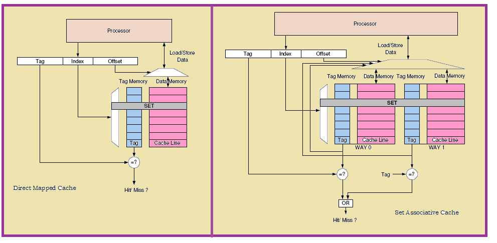 | Figure 7. Cache mapping techniques |
In sequential access, a 4-way-associative cache accesses one tag way after the other until someone hits or even the fourth one misses. On the other hand, phased caches wait until the tag array determines the matching way, and then accesses only the matching way of the data array, dissipating about 75% less energy than a parallel access cache. Sequential access, however, serializes the tag and data arrays, adding as much as 60% to the cache access time . If a tag memory block takes 1 cycle to be accessed, an eight way associative cache will take 8 cycles to detect a miss. Here arises the dilemma to decide between performance and memory block utilization.Existing methodologies employ the cache prediction by analyzing the likely hits. But our proposed methodology employ the utilization of the functions derived from the tag addresses for prediction. These functions are derived by the XOR operation of the address bytes (three MSBs). The following figure 8 shows the block diagram of the proposed methodology.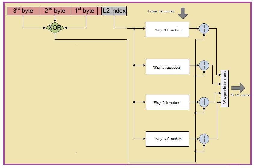 | Figure 8. Block diagram of the proposed methodology: XOR functionality |
The XOR function is implemented exclusively on the three MSBs of the address field because the respective functions can be stored in a SRAM module instead of searching all tags in parallel or employing prediction tables. The function here is assumed to be s simple checksum function. The comparison of this function with the actual address gives an indication for a specific way that is very much possible to generate a hit. The checksum function is selected in order to ensure that no false occurs while comparisons. This methodology is mainly developed to minimize the L2 cache access time which increases because of the sequential tag access. It employs the parallel access mechanism with L1 cache in such a way that no other extra cycle is consumed in L2 for the effective prediction. For its functional implementation, four unique memory modules are required one for each L2 cache way. Each entry consists of 1 byte, which is the size of each function. Each of the eight bit function is obtained from the XOR function of the three most significant bytes of the processor address. In order to predict the possible hit L2 ways, the three most significant bytes of the processor address are bitwise XORed and compared with the four functions, of the index relevant to the processor address. In case of a L2 miss the way prediction table has to be updated with the new function something that is responsible for the L2 cache controller.
6. Implementation
An FPGA prototype is implemented. For the validation of the proposed approach we have used Xilinx ISE 9.2i for simulation and synthesis purposes. Simulation results are shown in appendix. The following table 1 shows the memory module specifications:| Table 1. Memory module specifications |
| | S.No | Module | Clock frequency | Mapping | Size | | 1 | L1 Cache | 50 MHz | Direct | 4 KB | | 2 | L2 Cache | 50 MHz | 4 way Set associative | 64 KB | | 3 | Main memory | 100 MHz | - | 256 MB |
|
|
Resource utilization derived from the synthesis report is summarized as follows:| Table 2. Memory module Resource utilization |
| | S.No | Module | No. of LUTs | No. of FF | | 1 | L1 cache | 519 | 120 | | 2 | L2 cache | 1296 | 391 | | 3 | Main memory | 405 | 0 | | 4 | Prediction | 58 | 33 | | Total | 2278 | 544 |
|
|
A large part of the verification procedure was carried out in the implementation phase of the system. Each of the modules was intensively simulated to check as many cases as possible. Also, functional blocks of the system level architecture were integrated and simulated to check their functionality. The system level functionality was stretched out to cover all the various cases that it is supposed to support. Apart from conventional simulation test benches, the proposed methodology was tested in real time hardware using FPGA. Matrix multiplication algorithm with various sizes of workloads is validated.
7. Results
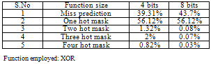
The following is the results analysis with the proposed XOR functionality:Task considered: Matrix multiplicationMiss rate = 43.8%Hit rate = 56.2%No. of accesses = 1039717Table 3. XOR functionality results
 |
| |
|
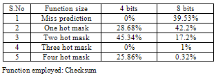
Table 4. Checksum functionality results
 |
| |
|
8. Conclusions
During the implementation a noteworthy issue is the decision of the function that will predict the possible hit L2 ways. XOR based way prediction generation mask algorithms compared with simple algorithms without functions on the address bits. Different sizes of checksum functions were compared each other to study their accuracy. The algorithm is false negative free. Miss prediction means when the prediction mask is all zeros, a miss is detected without tag matching. One hot mask means that the possible way the data located is only one. Two ones mask is with two possible hit ways and so on for the other two cases. It can be clearly observed that the 8 bits function is more accurate than the 4 bit function. It is noteworthy to observe the accuracy of the miss prediction. In matrix multiplication the miss rate is 43.8% of 1 million accesses and the predicted are 43.7% with XOR function and 39.53% without function. It is also remarkable to see that the accuracy of the 4bit XOR function is more efficient than the 8bits simple checksum function. Another observation concerns the hits. The 8bits XOR function predicts the only correct way (one hot mask) with great possibility, converting the 4-way associative cache to direct map in terms of power consumption without converting the cache to phased even it is behaved so. All these reasons lead us to choose the 8bit XOR-based function generation for the implementation.
References
| [1] | Srilatha C and Dr. Guru Rao CV, “A Novel Approach for Estimation and Optimization of Memory In Low Power Embedded Systems” International journal of computer theory and engineering, Vol. 1, No.5, December 2009, pages 578 – 585 |
| [2] | CHUANJUN ZHANG and FRANK VAHID and WALID NAJJAR, “A Highly Configurable Cache for Low Energy Embedded Systems” , ACM Transactions on Embedded Computing Systems, Vol. 4, No. 2, May 2005, Pages 363–387 |
| [3] | D. Gu, C. Verbrugge, and E. Gagnon. Relative factors in performance analysis of Java virtual machines. In VEE ’06, pages 111–121, New York, NY, USA, June 2006. ACM Press |
| [4] | K. Inoue, T. Ishihara, and K. Murakami, “Way-predicting set associative cache for high performance and low energy consumption,” Int’l Symposium on Low Power Electronic Design, 1999 |
| [5] | M.D. Powell, A. Agarwal, T.N. Vijaykumar, B. Falsafi, and K. Roy, “Reducing set-associative cache energy via way- prediction and selective direct-mapping,” 34th International Symposium on Micro architecture, 2001 |
| [6] | S. Ghosh, M. Martonosi, and S. Malik, “Cache Miss Equations: A Compiler Framework for Analyzing and Tuning Memory Behavior,” ACM Transactions on Programming Languages and Systems (TOPLAS), vol. 21, no. 4, pp. 703 - 746, July 1999 |
| [7] | W. Fornaciari et al., “A Design Framework to Efficiently Explore Energy-Delay Tradeoffs,” Proceedings of the ninth international symposium on Hardware/software codesign, pp. 260 - 265, Copenhagen, Denmark, 2001 |
| [8] | J. J. Pieper et al., “High Level Cache Simulation for Heterogeneous Multiprocessors,” Proceedings of the 41st annual conference on Design automation, pp. 287 - 292, San Diego, CA, USA, June 2004 |
| [9] | J. H. CHANG, H. CHAO, AND K. SO. Cache design of a sub-micron cmos system/ 370. In ISCA ’87: Proceedings of the 14th annual international symposium on Computer architecture, pages 208–213. ACM Press, 1987 |
| [10] | R.E. KESSLER, R. JOOSS, A. LEBECK, AND M.D. HILL. Inexpensive implementations of set-associativity. In Proc. 16th Int. Symp. on Computer Architecture (ISCA ’89), pages 131–139. ACM Press, May/June 1989 |
| [11] | LISHING LIU. Cache designs with partial address matching. In MICRO 27: Proceedings of the 27th annual international symposium on Microarchitecture, pages 128–136. ACM Press, 1994 |
| [12] | A. Milidonis, N. Alachiotis, V. Porpodas, H. Michail, A. P. Kakarountas, and C. E. Goutis. Interactive presentation: A decoupled architecture of processors with scratch-pad memory hierarchy. In DATE '07: Proceedings of the conference on Design, automation and test in Europe, pages 612{617, San Jose, CA, USA, 2007. EDA Consortium |
| [13] | P. R. Panda, N. D. Dutt, and A. Nicolau. On-chip vs. off-chip memory: the data partitioning problem in embedded processor-based systems. ACM Trans. Des. Autom. Electron. Syst., 5(3):682{704, 2000 |
 Abstract
 Reference
 Full-Text PDF
 Full-Text HTML